CSCE 211 Digital Design Lec 11 Flip Flop


- Slides: 39

CSCE 211 Digital Design Lec 11 Flip Flop Excitation Tables Topics n Sequential Circuits l SR Latch l Clocked SR l Master Slave n Master Slave VHDL Readings: 5. 4, 5. 9, 5. 10, 4. 4 – 1– October 21, 2015 CSCE 211 H Fall 2015

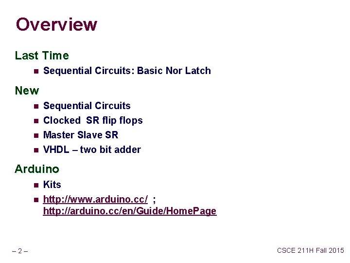
Overview Last Time n Sequential Circuits: Basic Nor Latch New n n Sequential Circuits Clocked SR flip flops Master Slave SR VHDL – two bit adder Arduino n n – 2– Kits http: //www. arduino. cc/ ; http: //arduino. cc/en/Guide/Home. Page CSCE 211 H Fall 2015

Register Bank - Mux – ALU - Decoder – 3– CSCE 211 H Fall 2015

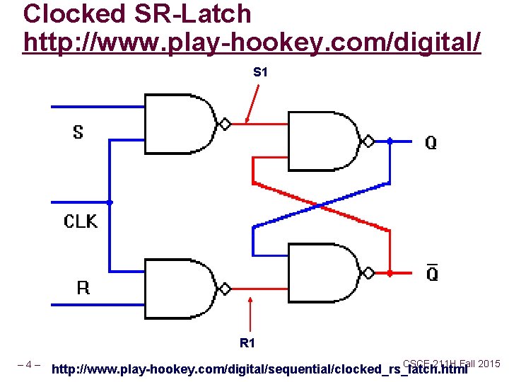
Clocked SR-Latch http: //www. play-hookey. com/digital/ S 1 R 1 – 4– CSCE 211 H Fall 2015 http: //www. play-hookey. com/digital/sequential/clocked_rs_latch. html

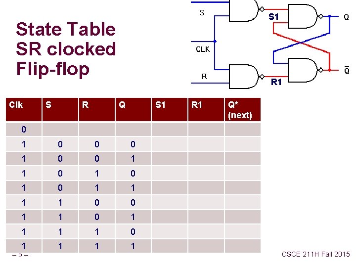
S 1 State Table SR clocked Flip-flop Clk S R R 1 Q S 1 R 1 Q* (next) 0 1 0 0 1 1 0 1 0 1 1 0 0 1 1 1 1 0 1 1 – 5– CSCE 211 H Fall 2015

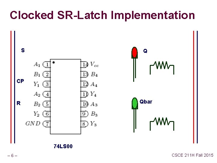
Clocked SR-Latch Implementation S Q CP Qbar R 74 LS 00 – 6– CSCE 211 H Fall 2015

74 LS 10 – 7– CSCE 211 H Fall 2015

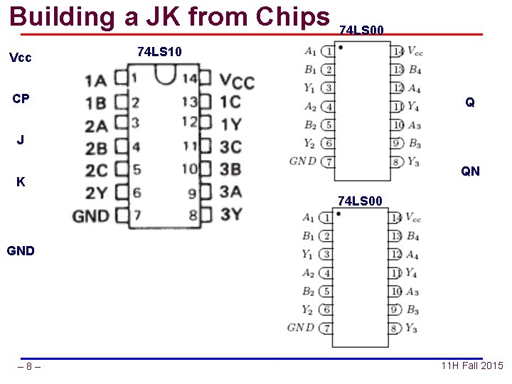
Building a JK from Chips Vcc 74 LS 00 74 LS 10 CP Q J QN K 74 LS 00 GND – 8– CSCE 211 H Fall 2015

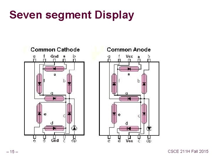
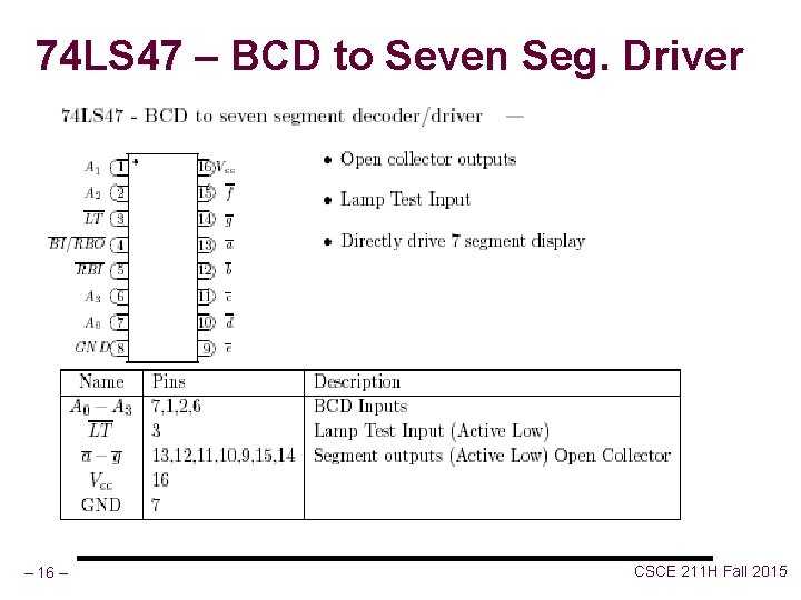
74 LS 49 – Seven segment display driver 74 LS 49/74 LS 47 n Inputs BCD digit (DCBA) (D is the MSB) n Outputs abcdefg – the seven segment driver lines Schematic fig 5 -45 n l Note negation of inputs to or-gate l x’ + y’ = (x’ + y’)’ ’ = (x’’. y’’)’ = (x. y)’ l It’s a NAND! n – 9– Truth table fig 5 -21 CSCE 211 H Fall 2015

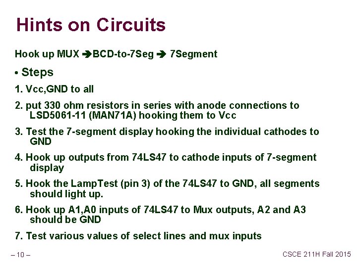
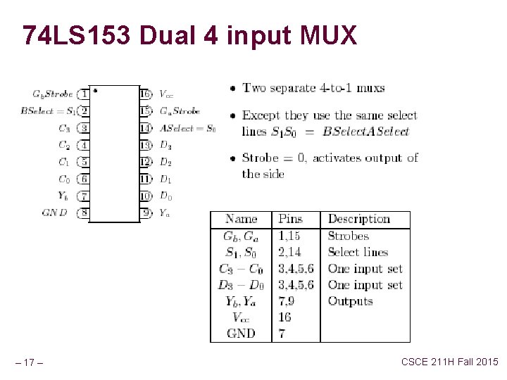
Hints on Circuits Hook up MUX BCD-to-7 Seg 7 Segment • Steps 1. Vcc, GND to all 2. put 330 ohm resistors in series with anode connections to LSD 5061 -11 (MAN 71 A) hooking them to Vcc 3. Test the 7 -segment display hooking the individual cathodes to GND 4. Hook up outputs from 74 LS 47 to cathode inputs of 7 -segment display 5. Hook the Lamp. Test (pin 3) of the 74 LS 47 to GND, all segments should light up. 6. Hook up A 1, A 0 inputs of 74 LS 47 to Mux outputs, A 2 and A 3 should be GND 7. Test various values of select lines and mux inputs – 10 – CSCE 211 H Fall 2015

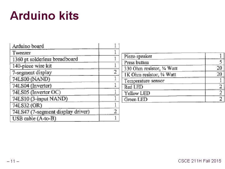
Arduino kits – 11 – CSCE 211 H Fall 2015

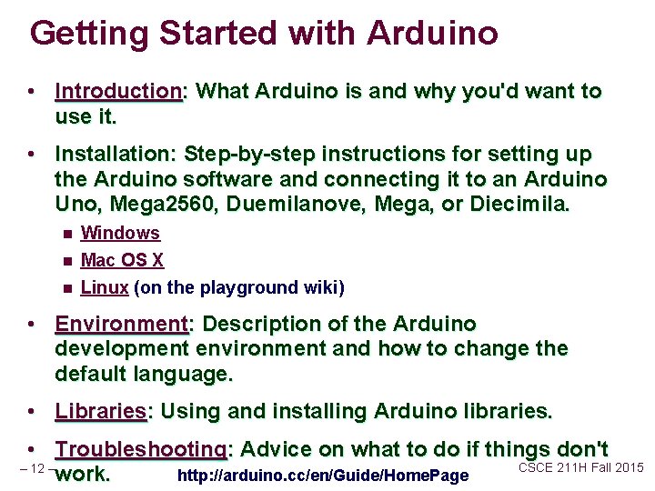
Getting Started with Arduino • Introduction: What Arduino is and why you'd want to use it. • Installation: Step-by-step instructions for setting up the Arduino software and connecting it to an Arduino Uno, Mega 2560, Duemilanove, Mega, or Diecimila. n n n Windows Mac OS X Linux (on the playground wiki) • Environment: Description of the Arduino development environment and how to change the default language. • Libraries: Using and installing Arduino libraries. • Troubleshooting: Advice on what to do if things don't CSCE 211 H Fall 2015 – 12 – http: //arduino. cc/en/Guide/Home. Page work.

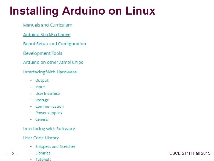
Installing Arduino on Linux – 13 – CSCE 211 H Fall 2015

Teams? 10 People; 5 teams – 14 – CSCE 211 H Fall 2015

Seven segment Display – 15 – CSCE 211 H Fall 2015

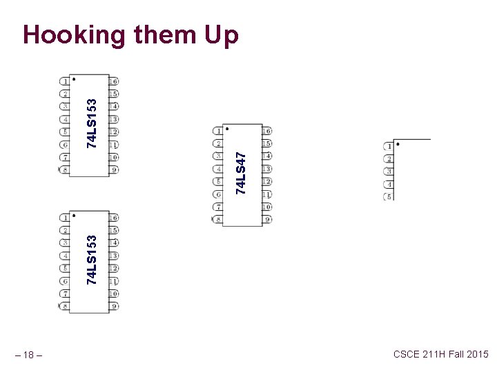
74 LS 47 – BCD to Seven Seg. Driver – 16 – CSCE 211 H Fall 2015

74 LS 153 Dual 4 input MUX – 17 – CSCE 211 H Fall 2015

74 LS 153 74 LS 47 74 LS 153 Hooking them Up – 18 – CSCE 211 H Fall 2015

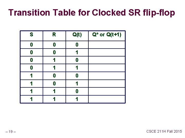
Transition Table for Clocked SR flip-flop – 19 – S R Q(t) 0 0 0 1 1 0 1 1 1 Q* or Q(t+1) CSCE 211 H Fall 2015

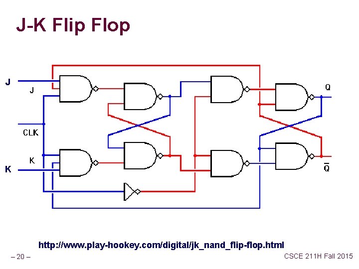
J-K Flip Flop J K http: //www. play-hookey. com/digital/jk_nand_flip-flop. html – 20 – CSCE 211 H Fall 2015

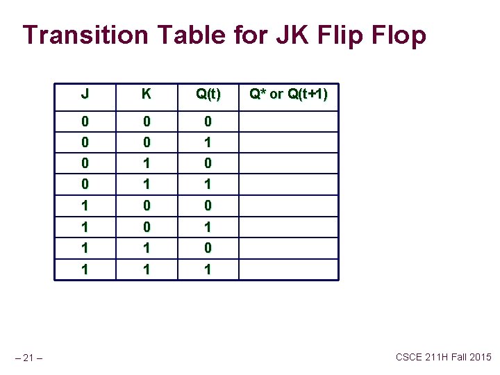
Transition Table for JK Flip Flop – 21 – J K Q(t) 0 0 0 1 1 0 1 1 1 Q* or Q(t+1) CSCE 211 H Fall 2015

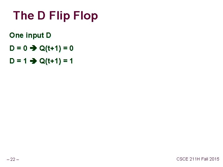
The D Flip Flop One input D D = 0 Q(t+1) = 0 D = 1 Q(t+1) = 1 – 22 – CSCE 211 H Fall 2015

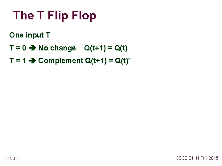
The T Flip Flop One input T T = 0 No change Q(t+1) = Q(t) T = 1 Complement Q(t+1) = Q(t)’ – 23 – CSCE 211 H Fall 2015

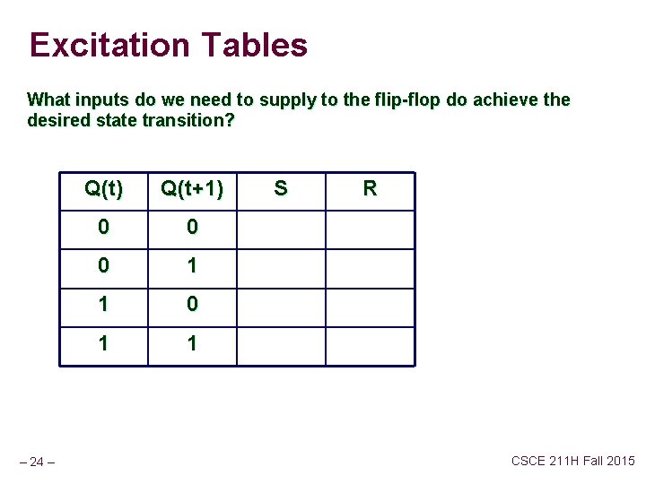
Excitation Tables What inputs do we need to supply to the flip-flop do achieve the desired state transition? – 24 – Q(t) Q(t+1) 0 0 0 1 1 S R CSCE 211 H Fall 2015

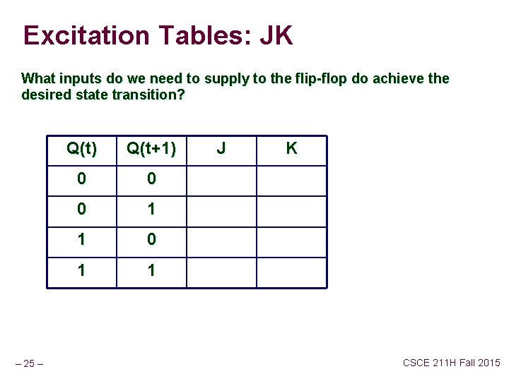
Excitation Tables: JK What inputs do we need to supply to the flip-flop do achieve the desired state transition? – 25 – Q(t) Q(t+1) 0 0 0 1 1 J K CSCE 211 H Fall 2015

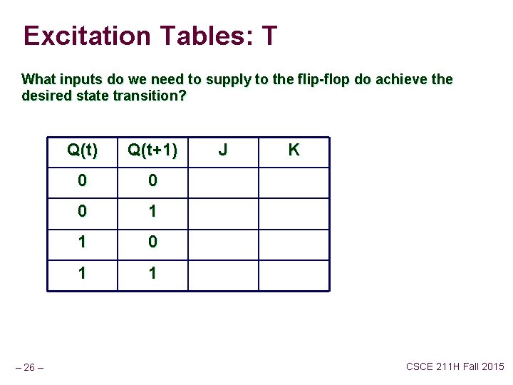
Excitation Tables: T What inputs do we need to supply to the flip-flop do achieve the desired state transition? – 26 – Q(t) Q(t+1) 0 0 0 1 1 J K CSCE 211 H Fall 2015

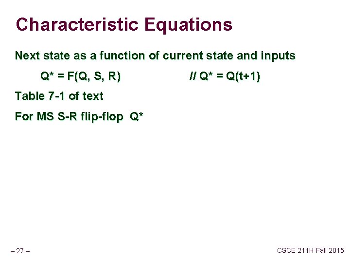
Characteristic Equations Next state as a function of current state and inputs Q* = F(Q, S, R) // Q* = Q(t+1) Table 7 -1 of text For MS S-R flip-flop Q* – 27 – CSCE 211 H Fall 2015

Characteristic Tables and Equations Characteristic Tables for a flip flop Describes next state Q* [or Q(t+1)] as function of inputs and in terms of current state Q [or Q(t)] Characteristic Equation specifies the next state as a function of current state and inputs (as an equation) – 28 – CSCE 211 H Fall 2015

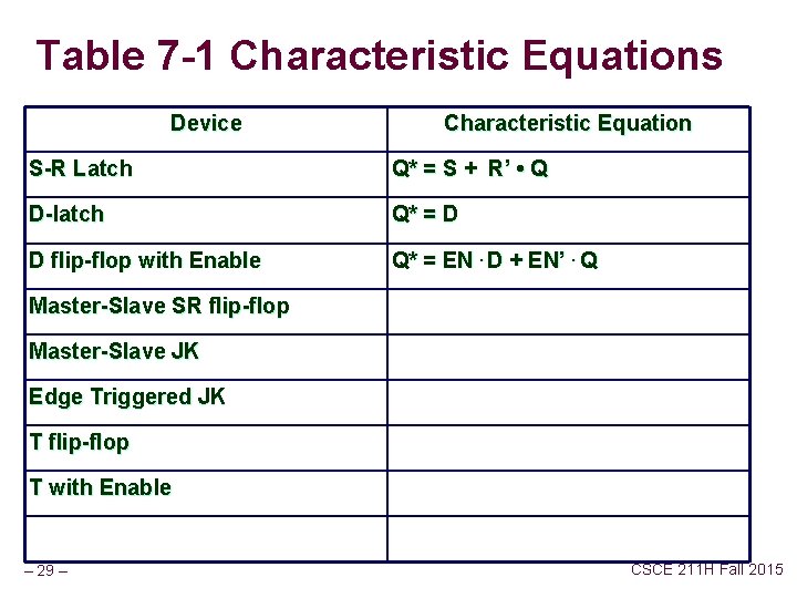
Table 7 -1 Characteristic Equations Device Characteristic Equation S-R Latch Q* = S + R’ • Q D-latch Q* = D D flip-flop with Enable Q* = EN. D + EN’. Q Master-Slave SR flip-flop Master-Slave JK Edge Triggered JK T flip-flop T with Enable – 29 – CSCE 211 H Fall 2015

Excitation Tables What inputs need to be given to cause a specific state transition? – 30 – CSCE 211 H Fall 2015

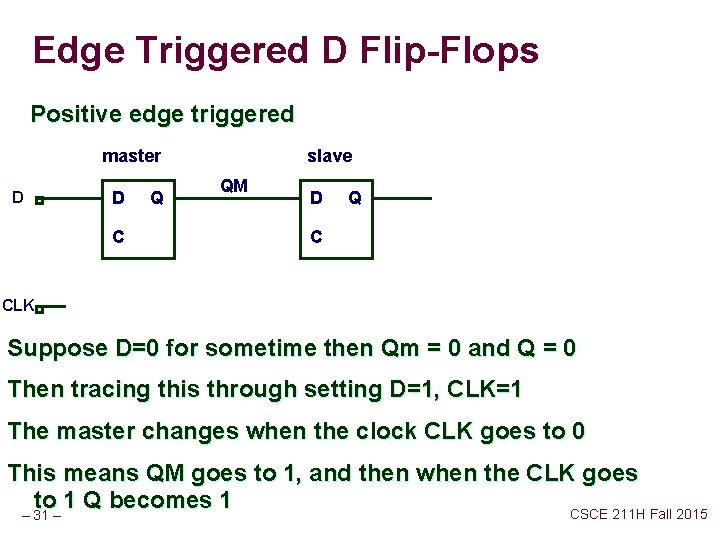
Edge Triggered D Flip-Flops Positive edge triggered master D D C Q slave QM D Q C CLK Suppose D=0 for sometime then Qm = 0 and Q = 0 Then tracing this through setting D=1, CLK=1 The master changes when the clock CLK goes to 0 This means QM goes to 1, and then when the CLK goes to 1 Q becomes 1 CSCE 211 H Fall 2015 – 31 –

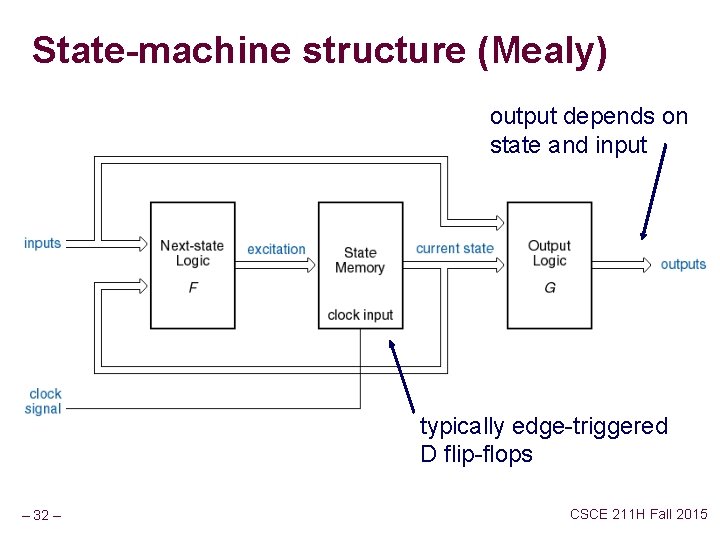
State-machine structure (Mealy) output depends on state and input typically edge-triggered D flip-flops – 32 – CSCE 211 H Fall 2015

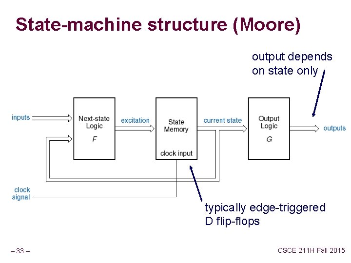
State-machine structure (Moore) output depends on state only typically edge-triggered D flip-flops – 33 – CSCE 211 H Fall 2015

TBird Lights State machine problem – 34 – CSCE 211 H Fall 2015

TBird Lights – 35 – CSCE 211 H Fall 2015

– 36 – CSCE 211 H Fall 2015

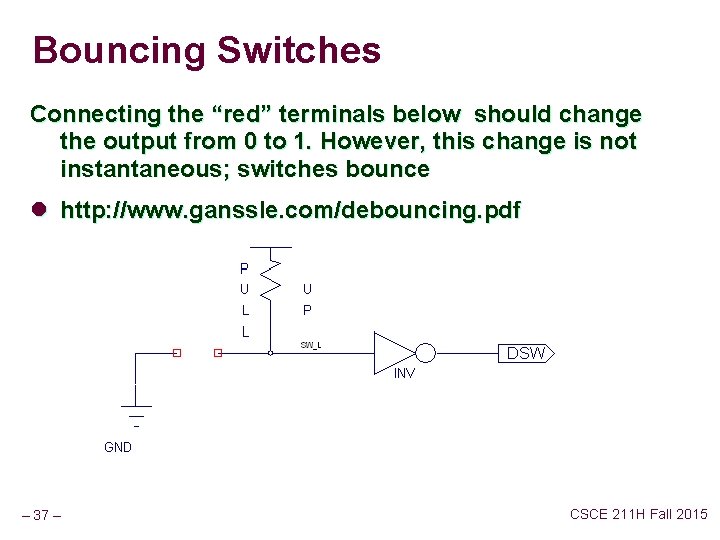
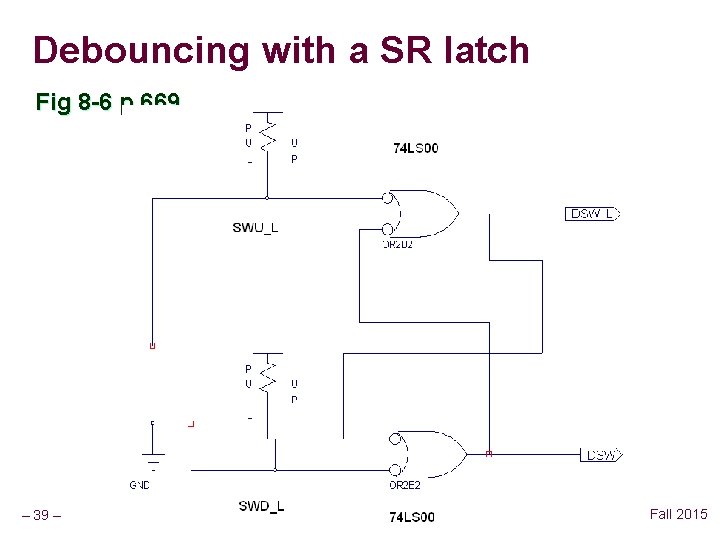
Bouncing Switches Connecting the “red” terminals below should change the output from 0 to 1. However, this change is not instantaneous; switches bounce l http: //www. ganssle. com/debouncing. pdf – 37 – CSCE 211 H Fall 2015

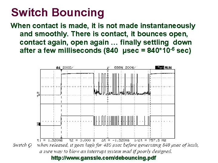
Switch Bouncing When contact is made, it is not made instantaneously and smoothly. There is contact, it bounces open, contact again, open again … finally settling down after a few milliseconds (840 μsec = 840*10 -6 sec) – 38 – http: //www. ganssle. com/debouncing. pdf CSCE 211 H Fall 2015

Debouncing with a SR latch Fig 8 -6 p 669 – 39 – CSCE 211 H Fall 2015