CSC 101 Introduction to Computing Lecture 11 Dr

- Slides: 41

CSC 101 Introduction to Computing Lecture 11 Dr. Iftikhar Azim Niaz ianiaz@comsats. edu. pk 1

Last Lecture Summary n Memory q n What memory stores q n ROM, PROM, EEPROM, Flash RAM – Volatile Memory q n Non Volatile and volatile Non Volatile q n OS, Application programs, Data, Instructions Types of Memory q n Address , size Static RAM, Dynamic RAM, MRAM SDRAM and its types 2

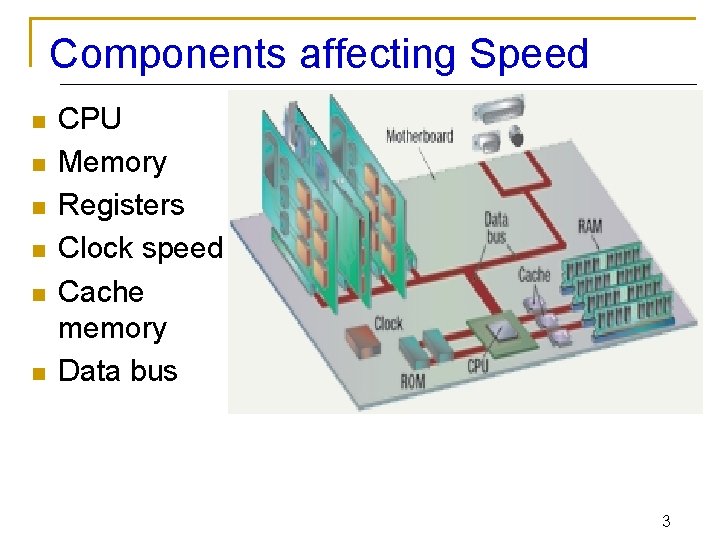
Components affecting Speed n n n CPU Memory Registers Clock speed Cache memory Data bus 3

Achieving Increased Processor n Speed Increase the hardware speed of the processor. q n Increasing the clock rate q n individual operations are executed more rapidly. Increase the size and speed of caches q q n shrinking the size of the logic gates on the processor chip, so that more gates can be packed together more tightly In particular, by dedicating a portion of the processor chip itself to the cache, cache access times drop significantly. Make changes to the processor organization and architecture that increase the effective speed of instruction execution. q Typically, this involves using parallelism in one form or another. 4

Registers n n processor contains small, high-speed storage locations temporarily hold data and instructions part of the processor, not part of memory or a permanent storage device. Different types of registers, each with a specific storage function including q q storing the location from where an instruction was fetched storing an instruction while the control unit decodes it storing data while the ALU computes it, and storing the results of a calculation. 5

Register Function n Almost all computers load data from a larger memory into registers where it is used for q q q n arithmetic, manipulated, or tested, by some machine instruction. Manipulated data is then often stored back in main memory, q q either by the same instruction or a subsequent one. 6

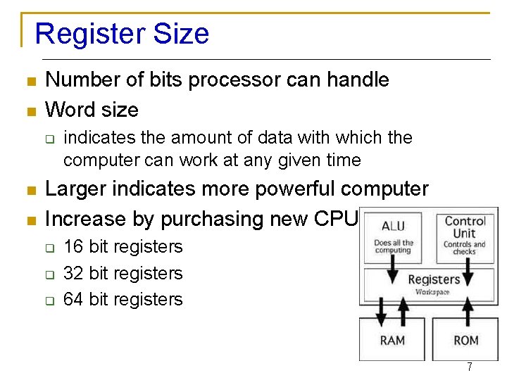
Register Size n n Number of bits processor can handle Word size q n n indicates the amount of data with which the computer can work at any given time Larger indicates more powerful computer Increase by purchasing new CPU q q q 16 bit registers 32 bit registers 64 bit registers 7

User Accessible Registers n Data registers q q n can hold numeric values such as integer and floating -point values, as well as characters, small bit arrays and other data. In some older CPUs, a special data register accumulator, is used implicitly for many operations. Address registers q hold addresses and are used by instructions that indirectly access main memory i. e. RAM 8

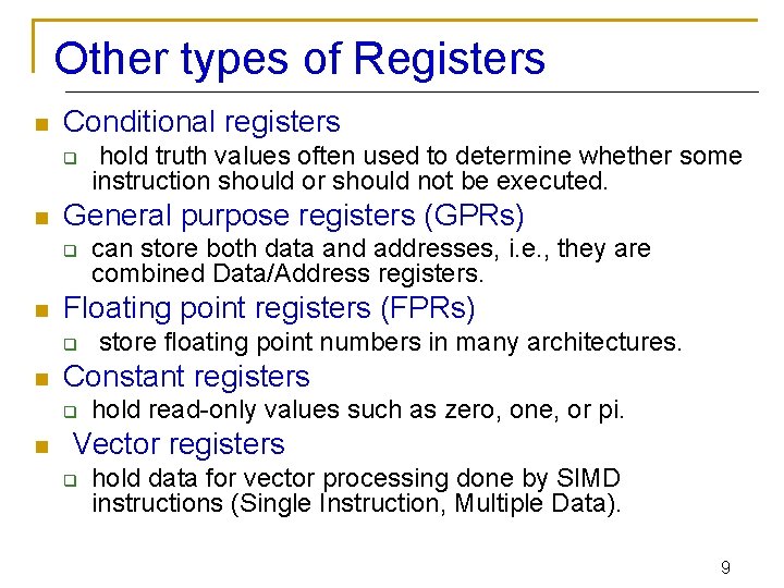
Other types of Registers n Conditional registers q n General purpose registers (GPRs) q n store floating point numbers in many architectures. Constant registers q n can store both data and addresses, i. e. , they are combined Data/Address registers. Floating point registers (FPRs) q n hold truth values often used to determine whether some instruction should or should not be executed. hold read-only values such as zero, one, or pi. Vector registers q hold data for vector processing done by SIMD instructions (Single Instruction, Multiple Data). 9

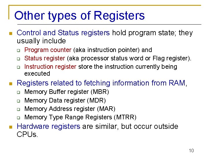
Other types of Registers n Control and Status registers hold program state; they usually include q q q n Registers related to fetching information from RAM, q q n Program counter (aka instruction pointer) and Status register (aka processor status word or Flag register). Instruction register store the instruction currently being executed Memory Buffer register (MBR) Memory Data register (MDR) Memory Address register (MAR) Memory Type Range Registers (MTRR) Hardware registers are similar, but occur outside CPUs. 10

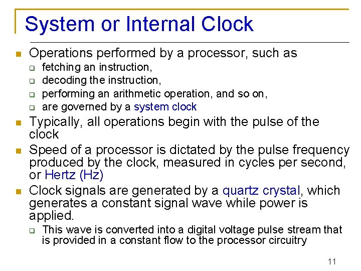
System or Internal Clock n Operations performed by a processor, such as q q n n n fetching an instruction, decoding the instruction, performing an arithmetic operation, and so on, are governed by a system clock Typically, all operations begin with the pulse of the clock Speed of a processor is dictated by the pulse frequency produced by the clock, measured in cycles per second, or Hertz (Hz) Clock signals are generated by a quartz crystal, which generates a constant signal wave while power is applied. q This wave is converted into a digital voltage pulse stream that is provided in a constant flow to the processor circuitry 11

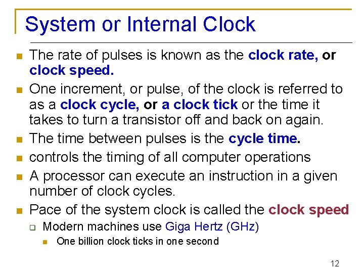
System or Internal Clock n n n The rate of pulses is known as the clock rate, or clock speed. One increment, or pulse, of the clock is referred to as a clock cycle, or a clock tick or the time it takes to turn a transistor off and back on again. The time between pulses is the cycle time. controls the timing of all computer operations A processor can execute an instruction in a given number of clock cycles. Pace of the system clock is called the clock speed q Modern machines use Giga Hertz (GHz) n One billion clock ticks in one second 12

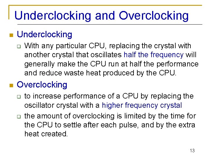
Underclocking and Overclocking n Underclocking q n With any particular CPU, replacing the crystal with another crystal that oscillates half the frequency will generally make the CPU run at half the performance and reduce waste heat produced by the CPU. Overclocking q q to increase performance of a CPU by replacing the oscillator crystal with a higher frequency crystal the amount of overclocking is limited by the time for the CPU to settle after each pulse, and by the extra heat created. 13

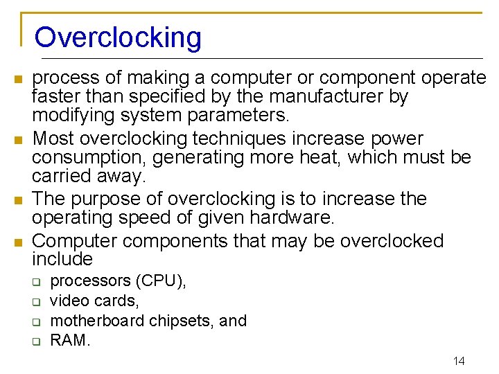
Overclocking n n process of making a computer or component operate faster than specified by the manufacturer by modifying system parameters. Most overclocking techniques increase power consumption, generating more heat, which must be carried away. The purpose of overclocking is to increase the operating speed of given hardware. Computer components that may be overclocked include q q processors (CPU), video cards, motherboard chipsets, and RAM. 14

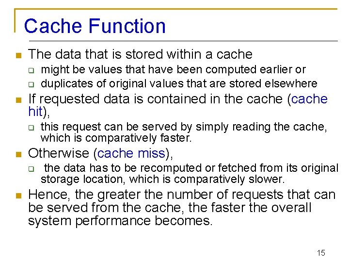
Cache Function n The data that is stored within a cache q q n If requested data is contained in the cache (cache hit), q n this request can be served by simply reading the cache, which is comparatively faster. Otherwise (cache miss), q n might be values that have been computed earlier or duplicates of original values that are stored elsewhere the data has to be recomputed or fetched from its original storage location, which is comparatively slower. Hence, the greater the number of requests that can be served from the cache, the faster the overall system performance becomes. 15

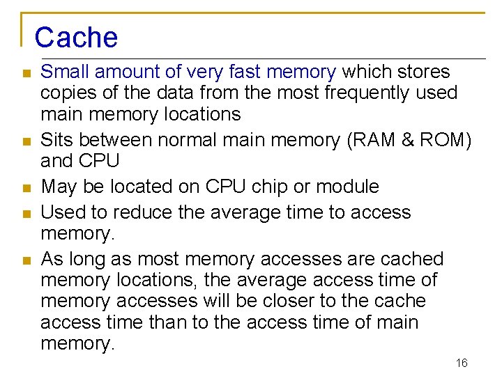
Cache n n n Small amount of very fast memory which stores copies of the data from the most frequently used main memory locations Sits between normal main memory (RAM & ROM) and CPU May be located on CPU chip or module Used to reduce the average time to access memory. As long as most memory accesses are cached memory locations, the average access time of memory accesses will be closer to the cache access time than to the access time of main memory. 16

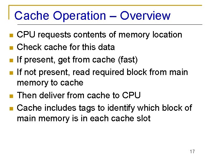
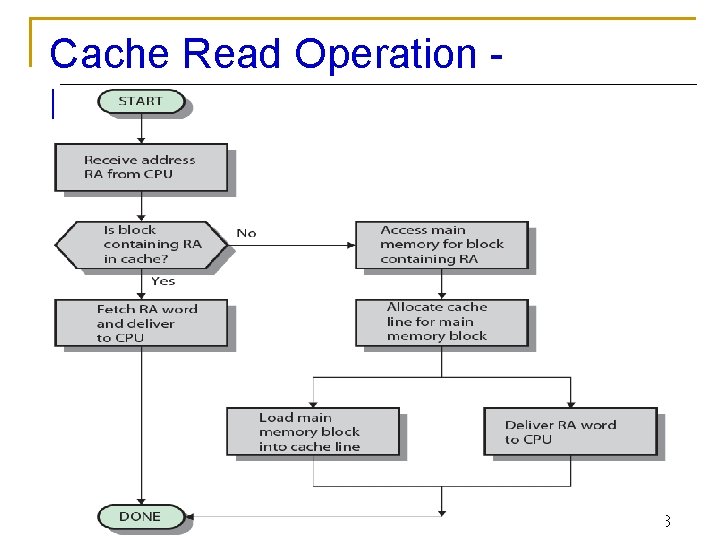
Cache Operation – Overview n n n CPU requests contents of memory location Check cache for this data If present, get from cache (fast) If not present, read required block from main memory to cache Then deliver from cache to CPU Cache includes tags to identify which block of main memory is in each cache slot 17

Cache Read Operation Flowchart 18

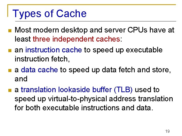
Types of Cache n n Most modern desktop and server CPUs have at least three independent caches: an instruction cache to speed up executable instruction fetch, a data cache to speed up data fetch and store, and a translation lookaside buffer (TLB) used to speed up virtual-to-physical address translation for both executable instructions and data. 19

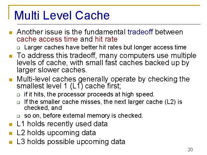
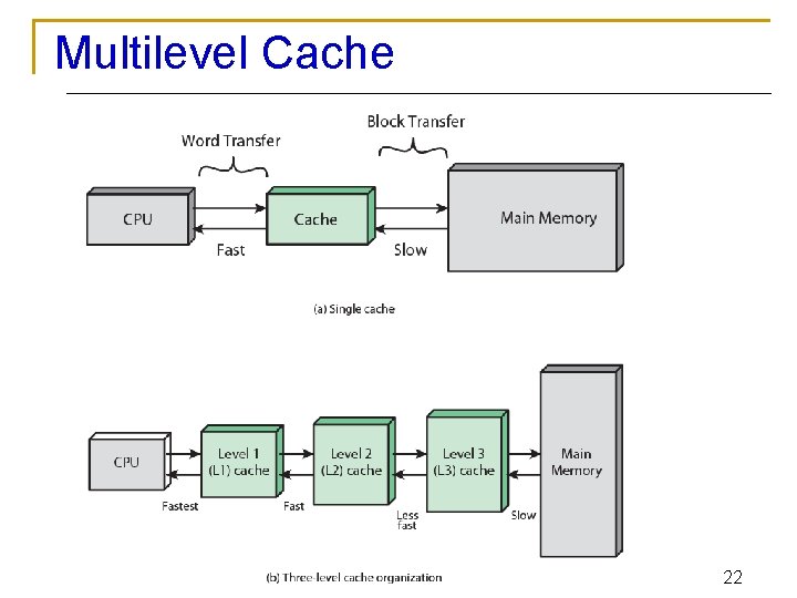
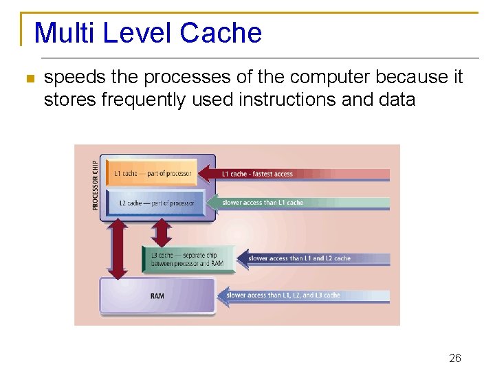
Multi Level Cache n Another issue is the fundamental tradeoff between cache access time and hit rate q n n To address this tradeoff, many computers use multiple levels of cache, with small fast caches backed up by larger slower caches. Multi-level caches generally operate by checking the smallest level 1 (L 1) cache first; q q q n n n Larger caches have better hit rates but longer access time if it hits, the processor proceeds at high speed. If the smaller cache misses, the next larger cache (L 2) is checked, and so on, before external memory is checked. L 1 holds recently used data L 2 holds upcoming data L 3 holds possible upcoming data 20

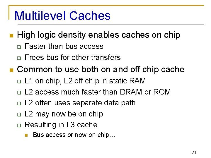
Multilevel Caches n High logic density enables caches on chip q q n Faster than bus access Frees bus for other transfers Common to use both on and off chip cache q q q L 1 on chip, L 2 off chip in static RAM L 2 access much faster than DRAM or ROM L 2 often uses separate data path L 2 may now be on chip Resulting in L 3 cache n Bus access or now on chip… 21

Multilevel Cache 22

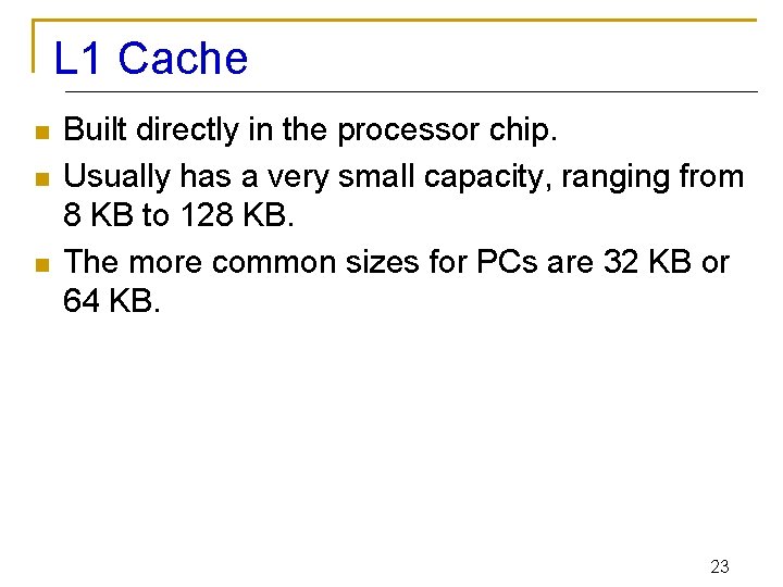
L 1 Cache n n n Built directly in the processor chip. Usually has a very small capacity, ranging from 8 KB to 128 KB. The more common sizes for PCs are 32 KB or 64 KB. 23

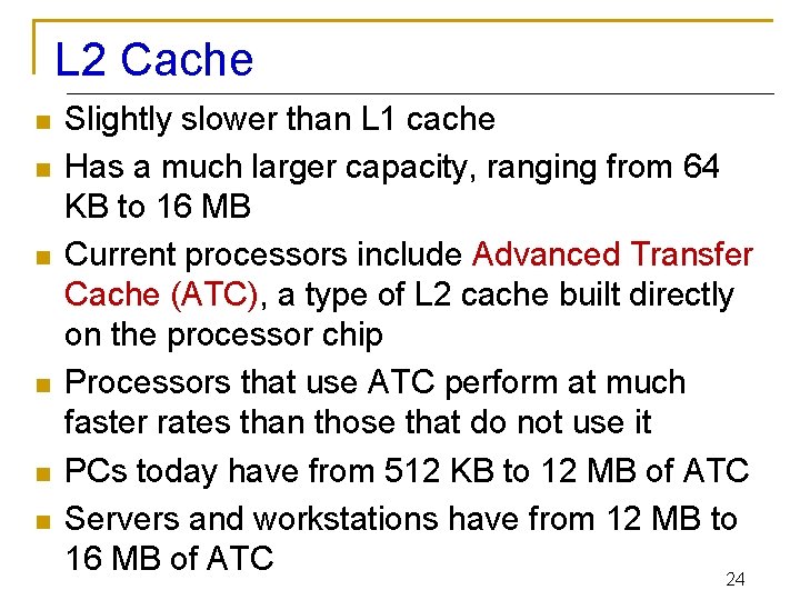
L 2 Cache n n n Slightly slower than L 1 cache Has a much larger capacity, ranging from 64 KB to 16 MB Current processors include Advanced Transfer Cache (ATC), a type of L 2 cache built directly on the processor chip Processors that use ATC perform at much faster rates than those that do not use it PCs today have from 512 KB to 12 MB of ATC Servers and workstations have from 12 MB to 16 MB of ATC 24

L 3 Cache n n n L 3 cache is a cache on the motherboard Separate from the processor chip. Exists only on computers that use L 2 Advanced Transfer Cache. Personal computers often have up to 8 MB of L 3 cache; Servers and work stations have from 8 MB to 24 MB of L 3 cache. 25

Multi Level Cache n speeds the processes of the computer because it stores frequently used instructions and data 26

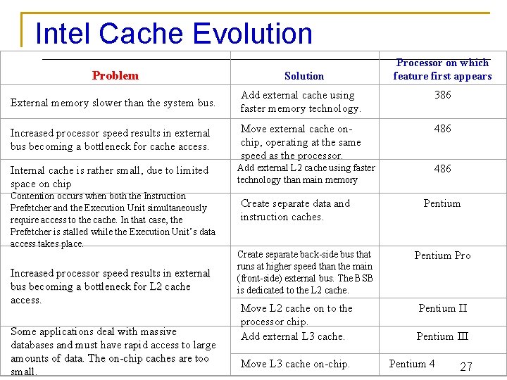
Intel Cache Evolution Problem Solution Processor on which feature first appears External memory slower than the system bus. Add external cache using faster memory technology. 386 Increased processor speed results in external bus becoming a bottleneck for cache access. Move external cache onchip, operating at the same speed as the processor. 486 Internal cache is rather small, due to limited space on chip Contention occurs when both the Instruction Prefetcher and the Execution Unit simultaneously require access to the cache. In that case, the Prefetcher is stalled while the Execution Unit’s data access takes place. Increased processor speed results in external bus becoming a bottleneck for L 2 cache access. Some applications deal with massive databases and must have rapid access to large amounts of data. The on-chip caches are too small. Add external L 2 cache using faster technology than main memory Create separate data and instruction caches. Create separate back-side bus that runs at higher speed than the main (front-side) external bus. The BSB is dedicated to the L 2 cache. Move L 2 cache on to the processor chip. Add external L 3 cache. Move L 3 cache on-chip. 486 Pentium Pro Pentium III Pentium 4 27

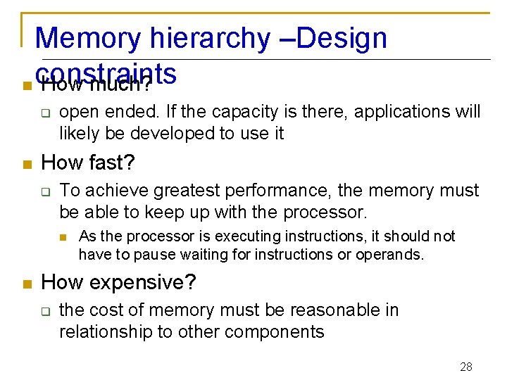
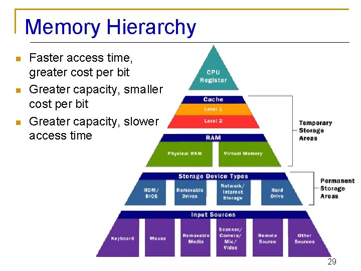
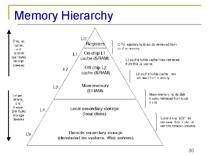
Memory hierarchy –Design n constraints How much? q n open ended. If the capacity is there, applications will likely be developed to use it How fast? q To achieve greatest performance, the memory must be able to keep up with the processor. n n As the processor is executing instructions, it should not have to pause waiting for instructions or operands. How expensive? q the cost of memory must be reasonable in relationship to other components 28

Memory Hierarchy n n n Faster access time, greater cost per bit Greater capacity, smaller cost per bit Greater capacity, slower access time 29

Memory Hierarchy 30

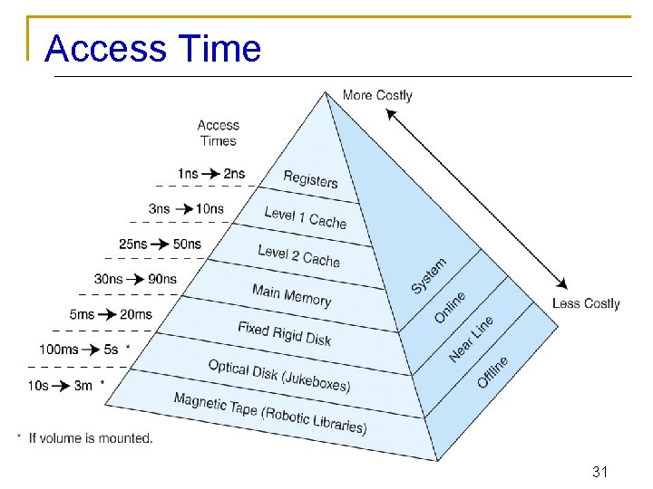
Access Time 31

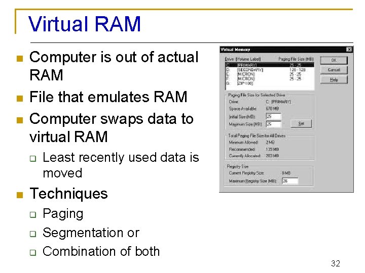
Virtual RAM n n n Computer is out of actual RAM File that emulates RAM Computer swaps data to virtual RAM q n Least recently used data is moved Techniques q q q Paging Segmentation or Combination of both 32

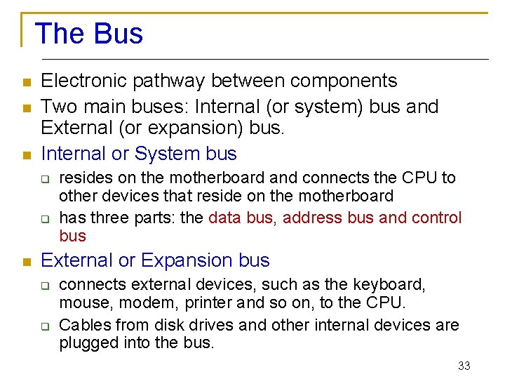
The Bus n n n Electronic pathway between components Two main buses: Internal (or system) bus and External (or expansion) bus. Internal or System bus q q n resides on the motherboard and connects the CPU to other devices that reside on the motherboard has three parts: the data bus, address bus and control bus External or Expansion bus q q connects external devices, such as the keyboard, mouse, modem, printer and so on, to the CPU. Cables from disk drives and other internal devices are plugged into the bus. 33

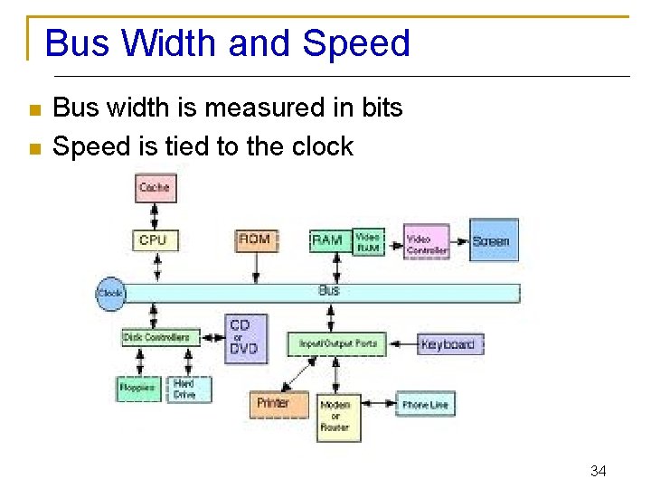
Bus Width and Speed n n Bus width is measured in bits Speed is tied to the clock 34

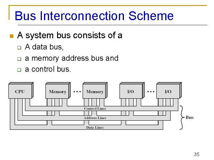
Bus Interconnection Scheme n A system bus consists of a q q q A data bus, a memory address bus and a control bus. 35

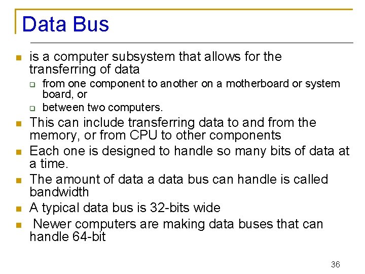
Data Bus n is a computer subsystem that allows for the transferring of data q q n n n from one component to another on a motherboard or system board, or between two computers. This can include transferring data to and from the memory, or from CPU to other components Each one is designed to handle so many bits of data at a time. The amount of data a data bus can handle is called bandwidth A typical data bus is 32 -bits wide Newer computers are making data buses that can handle 64 -bit 36

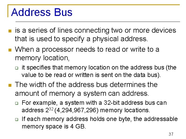
Address Bus n n is a series of lines connecting two or more devices that is used to specify a physical address. When a processor needs to read or write to a memory location, q n it specifies that memory location on the address bus (the value to be read or written is sent on the data bus). The width of the address bus determines the amount of memory a system can address. q q For example, a system with a 32 -bit address bus can address 232 (4, 294, 967, 296) memory locations. If each memory address holds one byte, the addressable memory space is 4 GB. 37

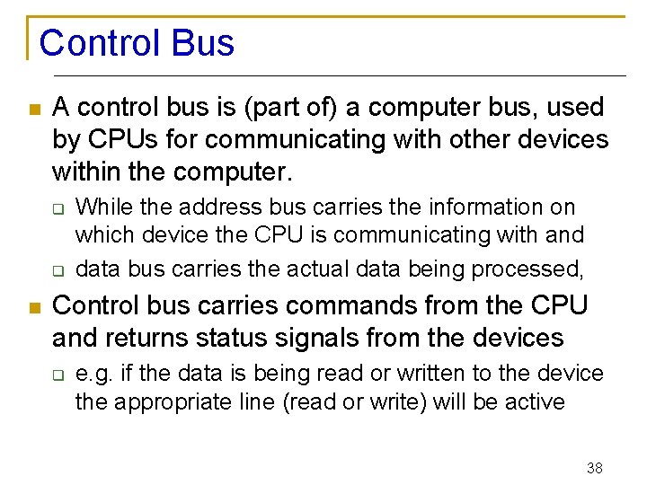
Control Bus n A control bus is (part of) a computer bus, used by CPUs for communicating with other devices within the computer. q q n While the address bus carries the information on which device the CPU is communicating with and data bus carries the actual data being processed, Control bus carries commands from the CPU and returns status signals from the devices q e. g. if the data is being read or written to the device the appropriate line (read or write) will be active 38

Summary I n n n Components Affecting Speed Achieving Increased Processor Speed Registers q q n Functions and Size User accessible and other types of Registers System or Internal Clock q q q Clock speed and clock rate Underclocking Overclocking 39

Summary II n Cache memory q q q Function operation Type: Instruction, data and TLB Multi Level Cache, L 1, L 2 and L 3 n q n Intel Cache Evolution Memory Hierarchy Bus q q Bus width and speed Bus Interconnection Scheme n Data, address and control bus 40

Recommended Websites n https: //en. wikipedia. org/wiki/Processor_register n https: //en. wikipedia. org/wiki/CPU_cache https: //en. wikipedia. org/wiki/Clock_rate https: //en. wikipedia. org/wiki/Bus_(computing) n n 41