CS 61 C Machine Structures Lecture 5 1



![Why is it “mem. Array[address[9: 2]]”? • Our memory is always byte-addressed • We Why is it “mem. Array[address[9: 2]]”? • Our memory is always byte-addressed • We](https://slidetodoc.com/presentation_image_h2/b411943bfbabc0e4a54c7f94d055fc6d/image-8.jpg)
![3 a: DE: Decode (Read Operands) • R[rd] = R[rs] op R[rt] Ex. : 3 a: DE: Decode (Read Operands) • R[rd] = R[rs] op R[rt] Ex. :](https://slidetodoc.com/presentation_image_h2/b411943bfbabc0e4a54c7f94d055fc6d/image-21.jpg)
![3 b: Add & Subtract • R[rd] = R[rs] op R[rt] Ex. : add. 3 b: Add & Subtract • R[rd] = R[rs] op R[rt] Ex. : add.](https://slidetodoc.com/presentation_image_h2/b411943bfbabc0e4a54c7f94d055fc6d/image-22.jpg)
![3 c: Logical Operations with Immediate • R[rt] = R[rs] op Zero. Ext[imm 16] 3 c: Logical Operations with Immediate • R[rt] = R[rs] op Zero. Ext[imm 16]](https://slidetodoc.com/presentation_image_h2/b411943bfbabc0e4a54c7f94d055fc6d/image-24.jpg)
![3 d: Load Operations • R[rt] = Mem[R[rs] + Sign. Ext[imm 16]] Example: lw 3 d: Load Operations • R[rt] = Mem[R[rs] + Sign. Ext[imm 16]] Example: lw](https://slidetodoc.com/presentation_image_h2/b411943bfbabc0e4a54c7f94d055fc6d/image-25.jpg)
![3 e: Store Operations • Mem[ R[rs] + Sign. Ext[imm 16] ] = R[rt] 3 e: Store Operations • Mem[ R[rs] + Sign. Ext[imm 16] ] = R[rt]](https://slidetodoc.com/presentation_image_h2/b411943bfbabc0e4a54c7f94d055fc6d/image-26.jpg)
- Slides: 33

CS 61 C : Machine Structures Lecture 5. 1. 2 CPU Design II 2004 -07 -20 Kurt Meinz inst. eecs. berkeley. edu/~cs 61 c CS 61 C L 5. 1. 2 CPU Design II (1) K. Meinz, Summer 2004 © UCB

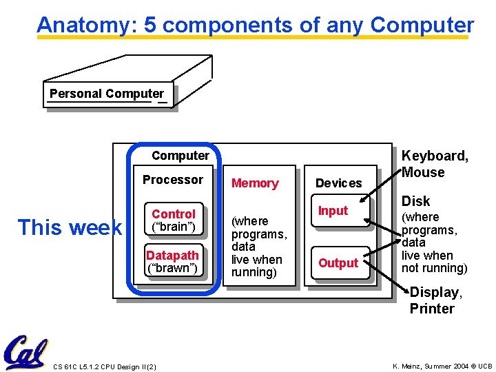
Anatomy: 5 components of any Computer Personal Computer Processor This week Control (“brain”) Datapath (“brawn”) Memory (where programs, data live when running) Devices Input Output Keyboard, Mouse Disk (where programs, data live when not running) Display, Printer CS 61 C L 5. 1. 2 CPU Design II (2) K. Meinz, Summer 2004 © UCB

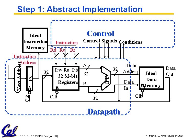
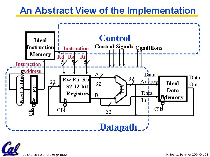
Step 1: Abstract Implementation Control PC Clk Next Address ALU Ideal Instruction Control Signals Conditions Memory Rd Rs Rt 5 5 5 Instruction Address A Data 32 Address Rw Ra Rb 32 Ideal Out 32 32 -bit 32 Data Registers B Memory In Clk 32 Clk Datapath CS 61 C L 5. 1. 2 CPU Design II (3) K. Meinz, Summer 2004 © UCB

Step 2 b: Components of the Datapath • Combinational Elements • Storage Elements • Clocking methodology CS 61 C L 5. 1. 2 CPU Design II (4) K. Meinz, Summer 2004 © UCB

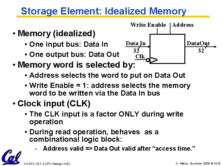
Storage Element: Idealized Memory Write Enable Address • Memory (idealized) Data In • One input bus: Data In 32 • One output bus: Data Out Clk Data. Out 32 • Memory word is selected by: • Address selects the word to put on Data Out • Write Enable = 1: address selects the memory word to be written via the Data In bus • Clock input (CLK) • The CLK input is a factor ONLY during write operation • During read operation, behaves as a combinational logic block: - Address valid => Data Out valid after “access time. ” CS 61 C L 5. 1. 2 CPU Design II (5) K. Meinz, Summer 2004 © UCB

Verilog Memory for MIPS Interpreter (1/3) //Behavioral modelof Random Access Memory: // 32 -bit wide, 256 words deep, // asynchronous read-port if RD=1, // synchronous write-port if WR=1, // initialize from hex file ("data. dat") // on positive edge of reset signal, // dump to binary file ("dump. dat") // on positive edge of dump signal. module mem (CLK, RST, DMP, WR, RD, address, write. D, read. D); input CLK, RST, DMP, WR, RD; input [31: 0] address, write. D; output [31: 0] read. D; reg [31: 0] read. D; parameter mem. Size=256; reg [31: 0] mem. Array [0: mem. Size-1]; integer chann, i; CS 61 C L 5. 1. 2 CPU Design II (6) K. Meinz, Summer 2004 © UCB

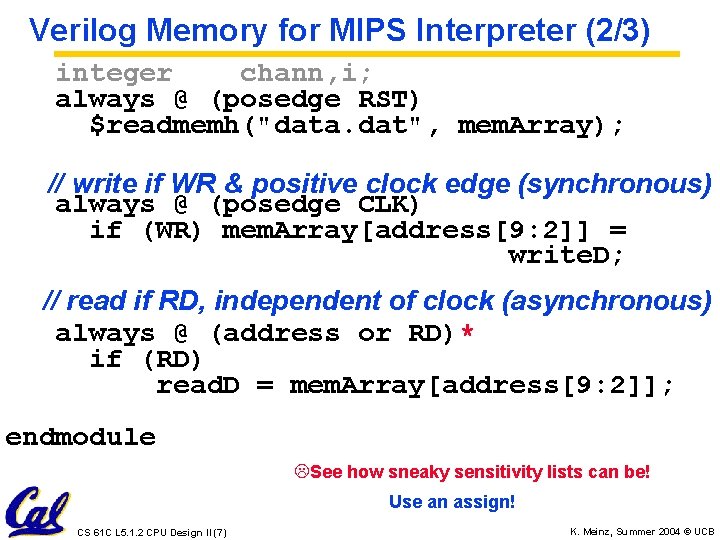
Verilog Memory for MIPS Interpreter (2/3) integer chann, i; always @ (posedge RST) $readmemh("data. dat", mem. Array); // write if WR & positive clock edge (synchronous) always @ (posedge CLK) if (WR) mem. Array[address[9: 2]] = write. D; // read if RD, independent of clock (asynchronous) always @ (address or RD)* if (RD) read. D = mem. Array[address[9: 2]]; endmodule LSee how sneaky sensitivity lists can be! Use an assign! CS 61 C L 5. 1. 2 CPU Design II (7) K. Meinz, Summer 2004 © UCB
![Why is it mem Arrayaddress9 2 Our memory is always byteaddressed We Why is it “mem. Array[address[9: 2]]”? • Our memory is always byte-addressed • We](https://slidetodoc.com/presentation_image_h2/b411943bfbabc0e4a54c7f94d055fc6d/image-8.jpg)
Why is it “mem. Array[address[9: 2]]”? • Our memory is always byte-addressed • We can lb from 0 x 0, 0 x 1, 0 x 2, 0 x 3, … • lw only reads word-aligned requests • We only call lw with 0 x 0, 0 x 4, 0 x 8, 0 x. C, … • I. e. , the last two bits are always 0 • mem. Array is a word wide and 28 deep • reg [31: 0] mem. Array [0: 256 -1]; • Size = 4 Bytes/row * 256 rows = 1024 B • If we’re simulating lw/sw, we R/W words • What bits select the first 256 words? [9: 2]! • 1 st word = 0 x 0 = 0 b 000 = mem. Array[0]; nd 2 word = 0 x 4 = 0 b 100 = mem. Array[1], etc. CS 61 C L 5. 1. 2 CPU Design II (8) K. Meinz, Summer 2004 © UCB

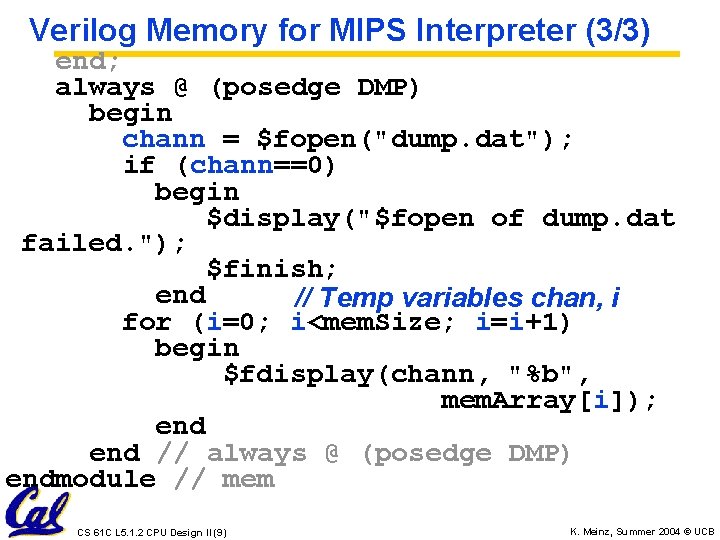
Verilog Memory for MIPS Interpreter (3/3) end; always @ (posedge DMP) begin chann = $fopen("dump. dat"); if (chann==0) begin $display("$fopen of dump. dat failed. "); $finish; end // Temp variables chan, i for (i=0; i<mem. Size; i=i+1) begin $fdisplay(chann, "%b", mem. Array[i]); end // always @ (posedge DMP) endmodule // mem CS 61 C L 5. 1. 2 CPU Design II (9) K. Meinz, Summer 2004 © UCB

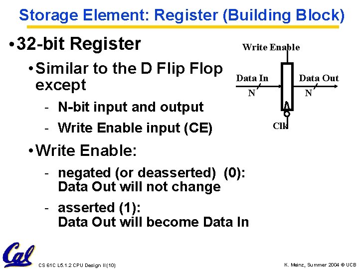
Storage Element: Register (Building Block) • 32 -bit Register • Similar to the D Flip Flop except Write Enable Data In N - N-bit input and output - Write Enable input (CE) Data Out N Clk • Write Enable: - negated (or deasserted) (0): Data Out will not change - asserted (1): Data Out will become Data In CS 61 C L 5. 1. 2 CPU Design II (10) K. Meinz, Summer 2004 © UCB

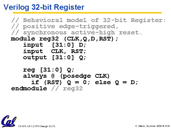
Verilog 32 -bit Register // Behavioral model of 32 -bit Register: // positive edge-triggered, // synchronous active-high reset. module reg 32 (CLK, Q, D, RST); input [31: 0] D; input CLK, RST; output [31: 0] Q; reg [31: 0] Q; always @ (posedge CLK) if (RST) Q = 0; else Q = D; endmodule // reg 32 CS 61 C L 5. 1. 2 CPU Design II (11) K. Meinz, Summer 2004 © UCB

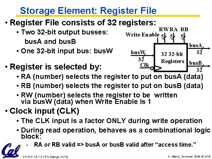
Storage Element: Register File • Register File consists of 32 registers: • Two 32 -bit output busses: bus. A and bus. B • One 32 -bit input bus: bus. W • Register is selected by: RWRA RB Write Enable 5 5 5 bus. W 32 Clk bus. A 32 32 32 -bit Registers bus. B 32 • RA (number) selects the register to put on bus. A (data) • RB (number) selects the register to put on bus. B (data) • RW (number) selects the register to be written via bus. W (data) when Write Enable is 1 • Clock input (CLK) • The CLK input is a factor ONLY during write operation • During read operation, behaves as a combinational logic block: - RA or RB valid => bus. A or bus. B valid after “access time. ” CS 61 C L 5. 1. 2 CPU Design II (12) K. Meinz, Summer 2004 © UCB

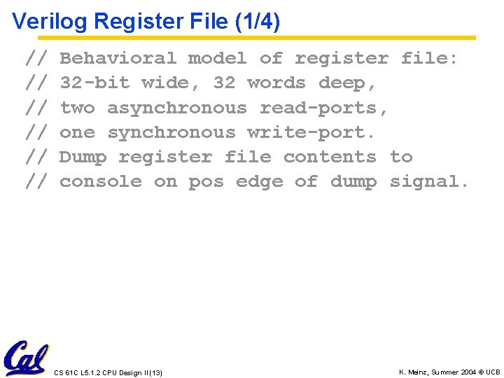
Verilog Register File (1/4) // // // Behavioral model of register file: 32 -bit wide, 32 words deep, two asynchronous read-ports, one synchronous write-port. Dump register file contents to console on pos edge of dump signal. CS 61 C L 5. 1. 2 CPU Design II (13) K. Meinz, Summer 2004 © UCB

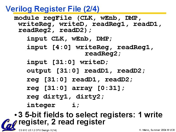
Verilog Register File (2/4) module reg. File (CLK, w. Enb, DMP, write. Reg, write. D, read. Reg 1, read. D 1, read. Reg 2, read. D 2); input CLK, w. Enb, DMP; input [4: 0] write. Reg, read. Reg 1, read. Reg 2; input [31: 0] write. D; output [31: 0] read. D 1, read. D 2; reg [31: 0] array [0: 31]; reg dirty 1, dirty 2; integer i; • 3 5 -bit fields to select registers: 1 write register, 2 read register CS 61 C L 5. 1. 2 CPU Design II (14) K. Meinz, Summer 2004 © UCB

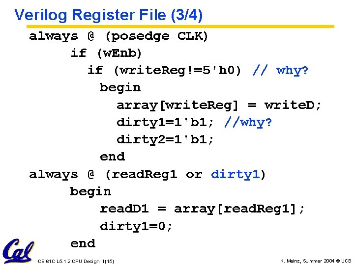
Verilog Register File (3/4) always @ (posedge CLK) if (w. Enb) if (write. Reg!=5'h 0) // why? begin array[write. Reg] = write. D; dirty 1=1'b 1; //why? dirty 2=1'b 1; end always @ (read. Reg 1 or dirty 1) begin read. D 1 = array[read. Reg 1]; dirty 1=0; end CS 61 C L 5. 1. 2 CPU Design II (15) K. Meinz, Summer 2004 © UCB

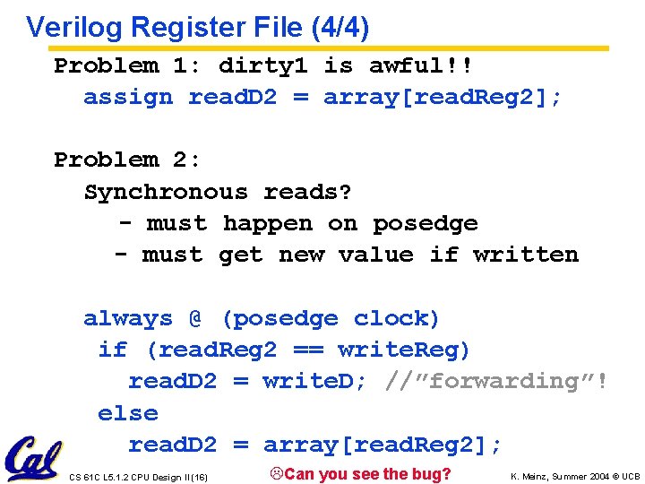
Verilog Register File (4/4) Problem 1: dirty 1 is awful!! assign read. D 2 = array[read. Reg 2]; Problem 2: Synchronous reads? - must happen on posedge - must get new value if written always @ (posedge clock) if (read. Reg 2 == write. Reg) read. D 2 = write. D; //”forwarding”! else read. D 2 = array[read. Reg 2]; CS 61 C L 5. 1. 2 CPU Design II (16) LCan you see the bug? K. Meinz, Summer 2004 © UCB

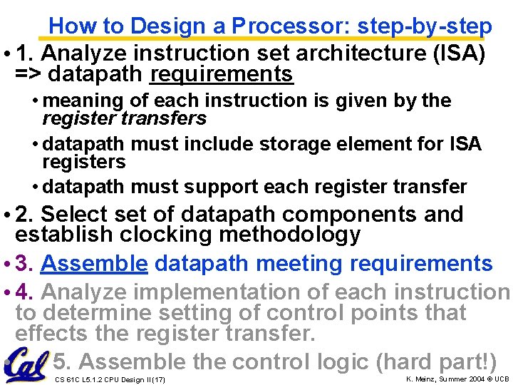
How to Design a Processor: step-by-step • 1. Analyze instruction set architecture (ISA) => datapath requirements • meaning of each instruction is given by the register transfers • datapath must include storage element for ISA registers • datapath must support each register transfer • 2. Select set of datapath components and establish clocking methodology • 3. Assemble datapath meeting requirements • 4. Analyze implementation of each instruction to determine setting of control points that effects the register transfer. • 5. Assemble the control logic (hard part!) CS 61 C L 5. 1. 2 CPU Design II (17) K. Meinz, Summer 2004 © UCB

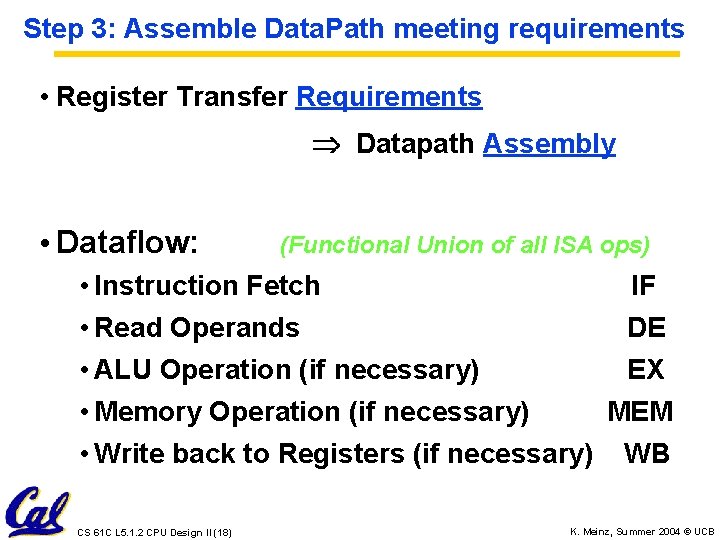
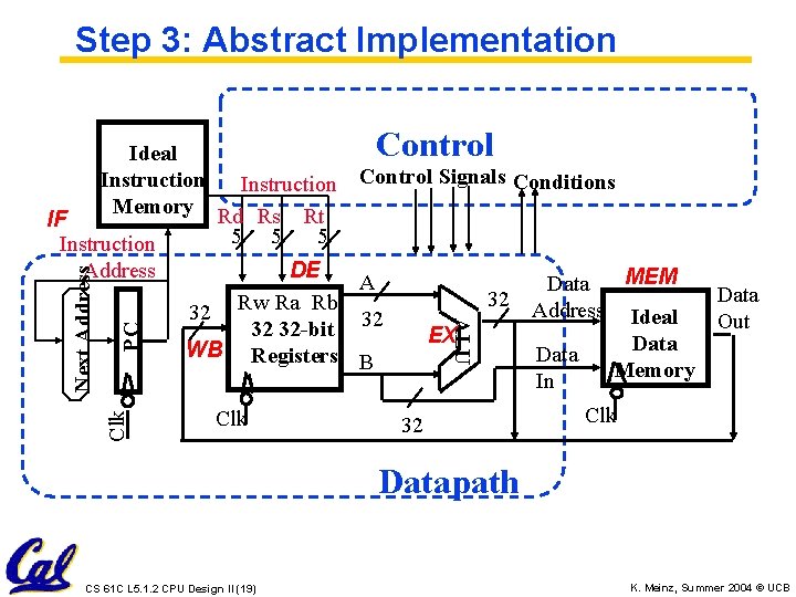
Step 3: Assemble Data. Path meeting requirements • Register Transfer Requirements Datapath Assembly • Dataflow: (Functional Union of all ISA ops) • Instruction Fetch IF • Read Operands DE • ALU Operation (if necessary) EX • Memory Operation (if necessary) MEM • Write back to Registers (if necessary) WB CS 61 C L 5. 1. 2 CPU Design II (18) K. Meinz, Summer 2004 © UCB

Step 3: Abstract Implementation Control PC Clk Next Address ALU Ideal Instruction Control Signals Conditions Memory Rd Rs Rt IF 5 5 5 Instruction Address DE MEM A Data 32 Address Rw Ra Rb 32 Ideal Out 32 32 -bit 32 EX Data WB Registers Data B Memory In Clk 32 Clk Datapath CS 61 C L 5. 1. 2 CPU Design II (19) K. Meinz, Summer 2004 © UCB

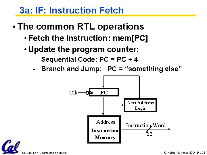
3 a: IF: Instruction Fetch • The common RTL operations • Fetch the Instruction: mem[PC] • Update the program counter: - Sequential Code: PC = PC + 4 - Branch and Jump: PC = “something else” Clk PC Next Address Logic Address Instruction Memory CS 61 C L 5. 1. 2 CPU Design II (20) Instruction Word 32 K. Meinz, Summer 2004 © UCB
![3 a DE Decode Read Operands Rrd Rrs op Rrt Ex 3 a: DE: Decode (Read Operands) • R[rd] = R[rs] op R[rt] Ex. :](https://slidetodoc.com/presentation_image_h2/b411943bfbabc0e4a54c7f94d055fc6d/image-21.jpg)
3 a: DE: Decode (Read Operands) • R[rd] = R[rs] op R[rt] Ex. : add. U rd, rs, rt • Ra, Rb, and Rw come from instruction’s Rs, Rt, 26 21 16 11 6 and Rd fields 31 op 6 bits 5 rt 5 bits rd 5 bits shamt 5 bits funct 6 bits Rs Rt 5 5 Rw Ra Rb Clk rs 5 bits 0 32 32 -bit Registers bus. A 32 bus. B 32 IF and DE are held in common for all ops. Now, we split up behavior by op type … CS 61 C L 5. 1. 2 CPU Design II (21) K. Meinz, Summer 2004 © UCB
![3 b Add Subtract Rrd Rrs op Rrt Ex add 3 b: Add & Subtract • R[rd] = R[rs] op R[rt] Ex. : add.](https://slidetodoc.com/presentation_image_h2/b411943bfbabc0e4a54c7f94d055fc6d/image-22.jpg)
3 b: Add & Subtract • R[rd] = R[rs] op R[rt] Ex. : add. U rd, rs, rt • ALUctr and Reg. Wr: control logic after decoding the instruction Rd Rs Rt Reg. Wr 5 5 5 32 32 -bit Registers bus. A 32 bus. B 32 ALU bus. W 32 Clk Rw Ra Rb ALUctr Result 32 • Already defined register file, ALU CS 61 C L 5. 1. 2 CPU Design II (22) K. Meinz, Summer 2004 © UCB

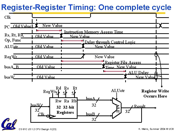
Register-Register Timing: One complete cycle Clk PC Old Value New Value Rs, Rt, Rd, Op, Func Old Value ALUctr Old Value Reg. Wr Old Value bus. A, B Old Value bus. W Old Value Instruction Memory Access Time New Value Delay through Control Logic New Value Register File Access Time New Value ALU Delay New Value Rd Rs Rt Reg. Wr 5 5 5 CS 61 C L 5. 1. 2 CPU Design II (23) bus. A 32 bus. B 32 ALU bus. W 32 Clk Rw Ra Rb 32 32 -bit Registers ALUctr Register Write Occurs Here Result 32 K. Meinz, Summer 2004 © UCB
![3 c Logical Operations with Immediate Rrt Rrs op Zero Extimm 16 3 c: Logical Operations with Immediate • R[rt] = R[rs] op Zero. Ext[imm 16]](https://slidetodoc.com/presentation_image_h2/b411943bfbabc0e4a54c7f94d055fc6d/image-24.jpg)
3 c: Logical Operations with Immediate • R[rt] = R[rs] op Zero. Ext[imm 16] 31 26 21 op 31 6 bits Rd Rt Reg. Dst Mux Rs Rt? Reg. Wr 5 5 5 32 Clk What about Rt register read? ? ALUct r bus. A 32 bus. B 32 Result 32 32 ALUSrc • Already defined 32 -bit MUX; Zero Ext? CS 61 C L 5. 1. 2 CPU Design II (24) 0 Mux 16 0 rt immediate 5 bits 16 15 rd? 16 bits immediate 00000000 16 bits Zero. Ext imm 16 11 rs 5 bits ALU bus. W Rw Ra Rb 32 32 -bit Registers 16 K. Meinz, Summer 2004 © UCB
![3 d Load Operations Rrt MemRrs Sign Extimm 16 Example lw 3 d: Load Operations • R[rt] = Mem[R[rs] + Sign. Ext[imm 16]] Example: lw](https://slidetodoc.com/presentation_image_h2/b411943bfbabc0e4a54c7f94d055fc6d/image-25.jpg)
3 d: Load Operations • R[rt] = Mem[R[rs] + Sign. Ext[imm 16]] Example: lw rt, rs, imm 16 31 26 op 6 bits Rd Reg. Dst Mux Reg. Wr 5 32 Clk rs 5 bits 0 rt 5 bits immediate 16 bits Rt Rs Rt? 5 5 Rw Ra Rb 32 32 -bit Registers W_Src 32 bus. B 32 32 Ext. Op 32 Mem. Wr ? ? ALUSrc Data In 32 Clk Mux CS 61 C L 5. 1. 2 CPU Design II (25) bus. A Mux 16 ALUctr Extender imm 16 16 ALU bus. W 21 Wr. En Adr Data Memory 32 K. Meinz, Summer 2004 © UCB
![3 e Store Operations Mem Rrs Sign Extimm 16 Rrt 3 e: Store Operations • Mem[ R[rs] + Sign. Ext[imm 16] ] = R[rt]](https://slidetodoc.com/presentation_image_h2/b411943bfbabc0e4a54c7f94d055fc6d/image-26.jpg)
3 e: Store Operations • Mem[ R[rs] + Sign. Ext[imm 16] ] = R[rt] Ex. : sw rt, rs, imm 16 31 26 21 op rs 6 bits 5 bits Rd Rt Reg. Dst Mux Reg. Wr 5 rt 5 bits immediate 16 bits ALUctr Mem. Wr W_Src 32 Ext. Op CS 61 C L 5. 1. 2 CPU Design II (26) 32 Mu x Extender 16 ALU bus. A Rw Ra Rb 32 32 32 -bit Registers bus. B 32 imm 16 0 Rs Rt 5 5 Mux bus. W 32 Clk 16 Data In 32 Clk Wr. En. Adr 32 Data Memory ALUSrc K. Meinz, Summer 2004 © UCB

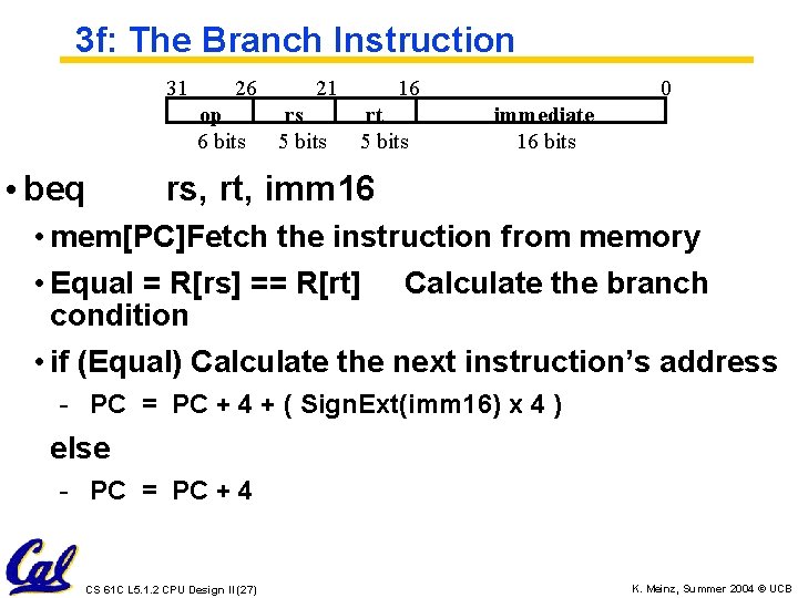
3 f: The Branch Instruction 31 26 op 6 bits • beq 21 rs 5 bits 16 rt 5 bits 0 immediate 16 bits rs, rt, imm 16 • mem[PC]Fetch the instruction from memory • Equal = R[rs] == R[rt] Calculate the branch condition • if (Equal) Calculate the next instruction’s address - PC = PC + 4 + ( Sign. Ext(imm 16) x 4 ) else - PC = PC + 4 CS 61 C L 5. 1. 2 CPU Design II (27) K. Meinz, Summer 2004 © UCB

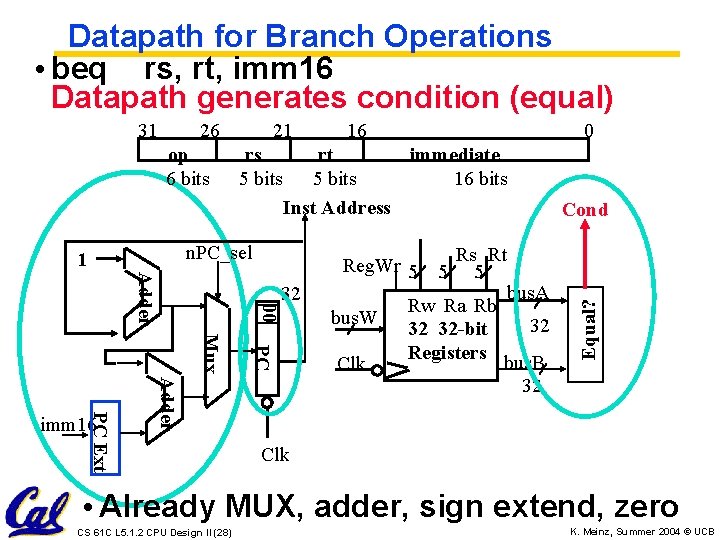
Datapath for Branch Operations • beq rs, rt, imm 16 Datapath generates condition (equal) 26 op 6 bits 21 rs 5 bits 00 Adder 32 PC Mux Adder PC Ext imm 16 0 immediate rt 5 bits 16 bits Inst Address n. PC_sel 1 16 Rs Rt 5 5 bus. A Rw Ra Rb 32 32 32 -bit Registers bus. B 32 Cond Reg. Wr 5 bus. W Clk Equal? 31 Clk • Already MUX, adder, sign extend, zero CS 61 C L 5. 1. 2 CPU Design II (28) K. Meinz, Summer 2004 © UCB

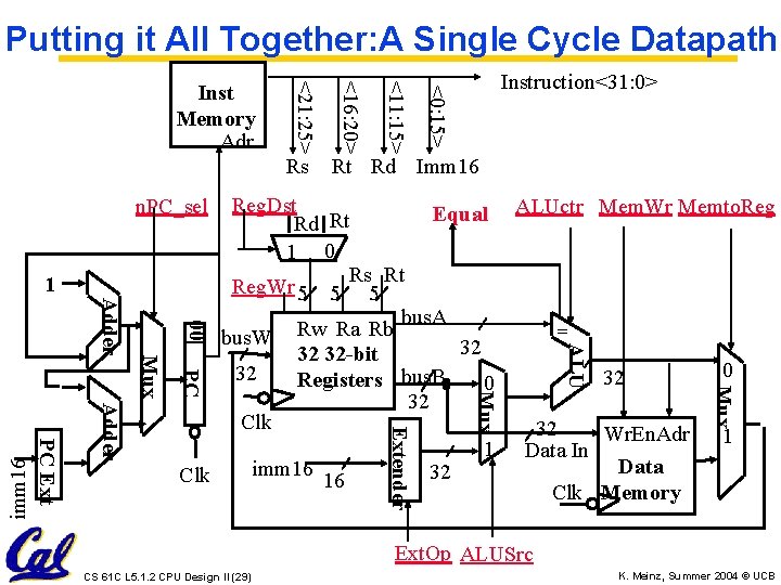
Putting it All Together: A Single Cycle Datapath Instruction<31: 0> <0: 15> <11: 15> Rs <16: 20> <21: 25> Inst Memory Adr Rt Rd Imm 16 Reg. Dst ALUctr Mem. Wr Memto. Reg Equal Rt Rd 1 0 Rs Rt Reg. Wr 5 5 5 bus. A Rw Ra Rb = bus. W 32 32 32 -bit 0 32 32 Registers bus. B 0 32 Clk 32 Wr. En. Adr 1 1 Data In Data imm 16 32 Clk 16 Clk Memory n. PC_sel imm 16 Mux ALU Extender PC Ext Adder Mux PC Mux Adder 00 1 Ext. Op ALUSrc CS 61 C L 5. 1. 2 CPU Design II (29) K. Meinz, Summer 2004 © UCB

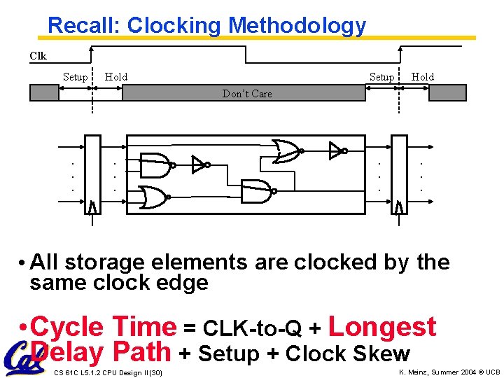
Recall: Clocking Methodology Clk Setup Hold . . . Don’t Care . . . • All storage elements are clocked by the same clock edge • Cycle Time = CLK-to-Q + Longest Delay Path + Setup + Clock Skew CS 61 C L 5. 1. 2 CPU Design II (30) K. Meinz, Summer 2004 © UCB

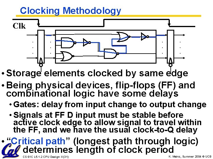
Clocking Methodology Clk. . . • Storage elements clocked by same edge • Being physical devices, flip-flops (FF) and combinational logic have some delays • Gates: delay from input change to output change • Signals at FF D input must be stable before active clock edge to allow signal to travel within the FF, and we have the usual clock-to-Q delay • “Critical path” (longest path through logic) determines length of clock period CS 61 C L 5. 1. 2 CPU Design II (31) K. Meinz, Summer 2004 © UCB

An Abstract View of the Implementation Control PC Clk Next Address ALU Ideal Instruction Control Signals Conditions Memory Rd Rs Rt 5 5 5 Instruction Address A Data 32 Address Rw Ra Rb 32 Ideal Out 32 32 -bit 32 Data Registers B Memory In Clk 32 Clk Datapath CS 61 C L 5. 1. 2 CPU Design II (32) K. Meinz, Summer 2004 © UCB

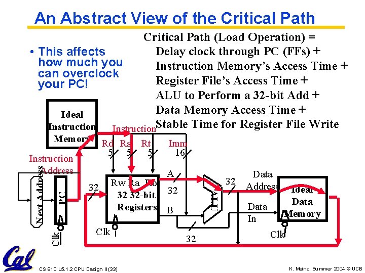
An Abstract View of the Critical Path (Load Operation) = Delay clock through PC (FFs) + • This affects how much you Instruction Memory’s Access Time + can overclock Register File’s Access Time + your PC! ALU to Perform a 32 -bit Add + Data Memory Access Time + Ideal Instruction. Stable Time for Register File Write Memory Rd Rs Rt 5 5 5 PC Clk A 32 Rw Ra Rb 32 32 -bit 32 Registers B Clk CS 61 C L 5. 1. 2 CPU Design II (33) ALU Next Address Instruction Address Imm 16 32 Data 32 Address Data In Ideal Data Memory Clk K. Meinz, Summer 2004 © UCB