CS 61 C Great Ideas in Computer Architecture


- Slides: 49

CS 61 C: Great Ideas in Computer Architecture Flip-Flops, FSMs, Logisim, Muxes Instructor: David A. Patterson http: //inst. eecs. Berkeley. edu/~cs 61 c/sp 12 10/3/2020 Spring 2012 -- Lecture #18 1

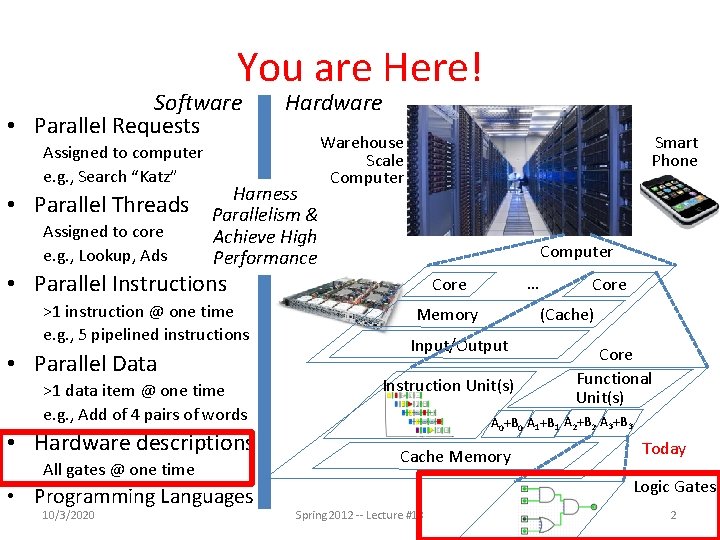
You are Here! Software • Parallel Requests Assigned to computer e. g. , Search “Katz” • Parallel Threads Assigned to core e. g. , Lookup, Ads Hardware Harness Parallelism & Achieve High Performance Smart Phone Warehouse Scale Computer • Parallel Instructions >1 instruction @ one time e. g. , 5 pipelined instructions • Parallel Data >1 data item @ one time e. g. , Add of 4 pairs of words • Hardware descriptions All gates @ one time • Programming Languages 10/3/2020 … Core Memory Core (Cache) Input/Output Instruction Unit(s) Core Functional Unit(s) A 0+B 0 A 1+B 1 A 2+B 2 A 3+B 3 Cache Memory Today Logic Gates Spring 2012 -- Lecture #18 2

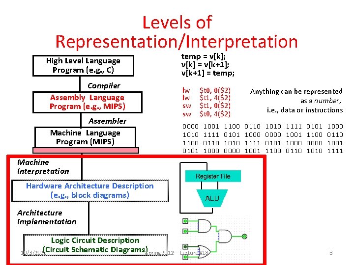
Levels of Representation/Interpretation High Level Language Program (e. g. , C) Compiler Assembly Language Program (e. g. , MIPS) Assembler Machine Language Program (MIPS) temp = v[k]; v[k] = v[k+1]; v[k+1] = temp; lw lw sw sw 0000 1010 1100 0101 $t 0, 0($2) $t 1, 4($2) $t 1, 0($2) $t 0, 4($2) 1001 1111 0110 1000 1100 0101 1010 0000 Anything can be represented as a number, i. e. , data or instructions 0110 1000 1111 1001 1010 0000 0101 1100 1111 1000 0110 0101 1100 0000 1010 1000 0110 1001 1111 Machine Interpretation Hardware Architecture Description (e. g. , block diagrams) Architecture Implementation Logic Circuit Description (Circuit Schematic Diagrams)Spring 2012 -- Lecture #18 10/3/2020 3

Review • Real world voltages are analog, but are quantized to represent logic 0 and logic 1 • Transistors are just switches, combined to form gates: AND, OR, NOT, NAND, NOR • Truth table can be mapped to gates for combinational logic design • Boolean algebra allows minimization of gates 10/3/2020 Spring 2012 -- Lecture #17 4

Agenda • • State Elements Administrivia Finite State Machines Introduction to Logisim Multiplexer ALU Design Summary 10/3/2020 Spring 2012 -- Lecture #18 5

Type of Circuits • Synchronous Digital Systems consist of two basic types of circuits: • Combinational Logic (CL) circuits – Output is a function of the inputs only, not the history of its execution – E. g. , circuits to add A, B (ALUs) – Last lecture was CL • Sequential Logic (SL) • • 10/3/2020 Circuits that “remember” or store information aka “State Elements” E. g. , memories and registers (Registers) Today’s lecture is SL Spring 2012 -- Lecture #17 6

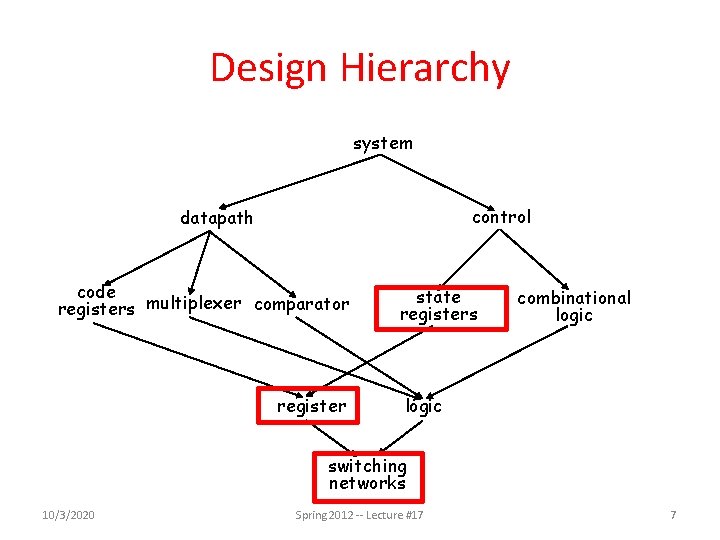
Design Hierarchy system control datapath code registers multiplexer comparator register state registers combinational logic switching networks 10/3/2020 Spring 2012 -- Lecture #17 7

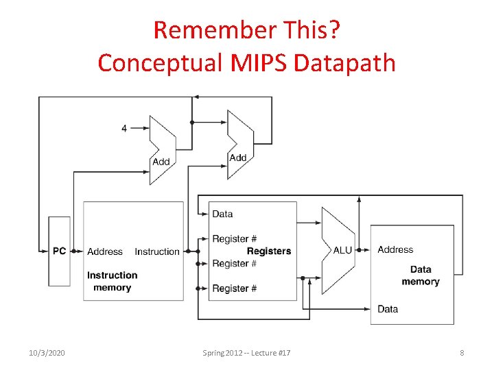
Remember This? Conceptual MIPS Datapath 10/3/2020 Spring 2012 -- Lecture #17 8

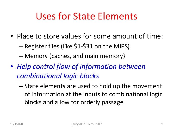
Uses for State Elements • Place to store values for some amount of time: – Register files (like $1 -$31 on the MIPS) – Memory (caches, and main memory) • Help control flow of information between combinational logic blocks – State elements are used to hold up the movement of information at the inputs to combinational logic blocks and allow for orderly passage 10/3/2020 Spring 2012 -- Lecture #17 9

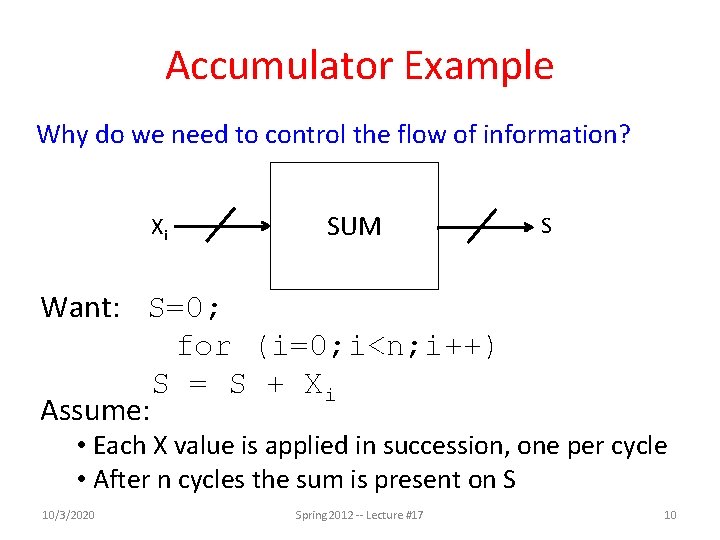
Accumulator Example Why do we need to control the flow of information? Xi SUM S Want: S=0; for (i=0; i<n; i++) S = S + Xi Assume: • Each X value is applied in succession, one per cycle • After n cycles the sum is present on S 10/3/2020 Spring 2012 -- Lecture #17 10

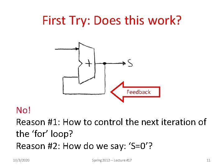
First Try: Does this work? Feedback No! Reason #1: How to control the next iteration of the ‘for’ loop? Reason #2: How do we say: ‘S=0’? 10/3/2020 Spring 2012 -- Lecture #17 11

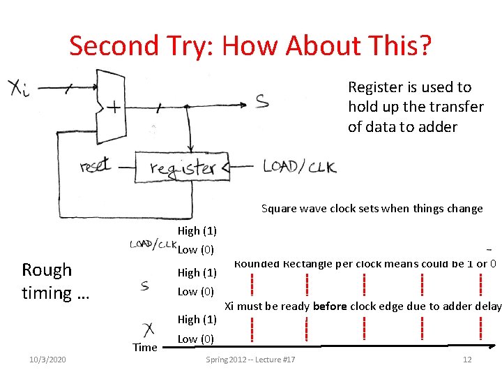
Second Try: How About This? Register is used to hold up the transfer of data to adder Square wave clock sets when things change High (1) Low (0) Rough timing … High (1) Low (0) High (1) 10/3/2020 Time Rounded Rectangle per clock means could be 1 or 0 Xi must be ready before clock edge due to adder delay Low (0) Spring 2012 -- Lecture #17 12

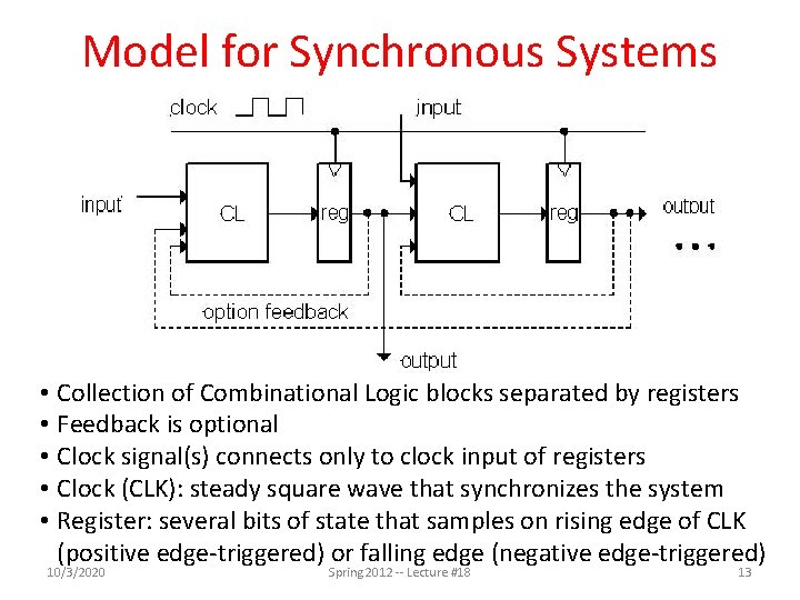
Model for Synchronous Systems • Collection of Combinational Logic blocks separated by registers • Feedback is optional • Clock signal(s) connects only to clock input of registers • Clock (CLK): steady square wave that synchronizes the system • Register: several bits of state that samples on rising edge of CLK (positive edge-triggered) or falling edge (negative edge-triggered) 10/3/2020 Spring 2012 -- Lecture #18 13

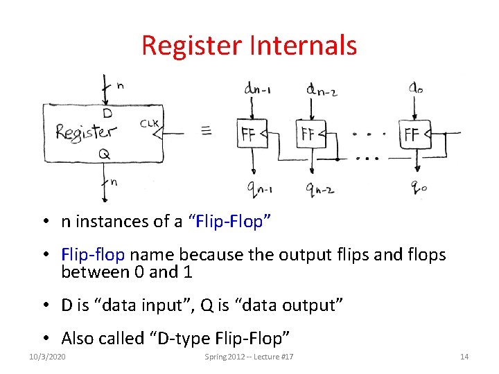
Register Internals • n instances of a “Flip-Flop” • Flip-flop name because the output flips and flops between 0 and 1 • D is “data input”, Q is “data output” • Also called “D-type Flip-Flop” 10/3/2020 Spring 2012 -- Lecture #17 14

Camera Analogy Timing Terms • Want to take a portrait – timing right before and after taking picture • Set up time – don’t move since about to take picture (open camera shutter) • Hold time – need to hold still after shutter opens until camera shutter closes • Time click to data – time from open shutter until can see image on output (viewfinder) 10/3/2020 Spring 2012 -- Lecture #18 15

Hardware Timing Terms • Setup Time: when the input must be stable before the edge of the CLK • Hold Time: when the input must be stable after the edge of the CLK • “CLK-to-Q” Delay: how long it takes the output to change, measured from the edge of the CLK 10/3/2020 Spring 2012 -- Lecture #18 16

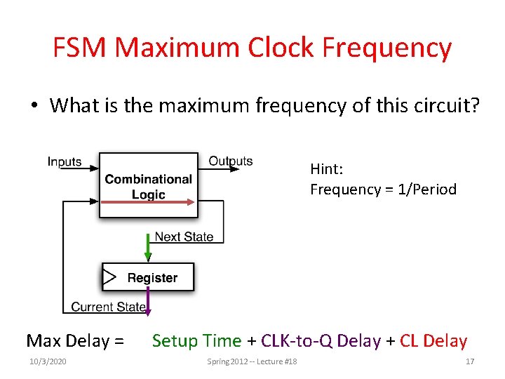
FSM Maximum Clock Frequency • What is the maximum frequency of this circuit? Hint: Frequency = 1/Period Max Delay = 10/3/2020 Setup Time + CLK-to-Q Delay + CL Delay Spring 2012 -- Lecture #18 17

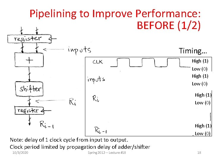
Pipelining to Improve Performance: BEFORE (1/2) Timing… High (1) Low (0) Note: delay of 1 clock cycle from input to output. Clock period limited by propagation delay of adder/shifter 10/3/2020 Spring 2012 -- Lecture #18 High (1) Low (0) 18

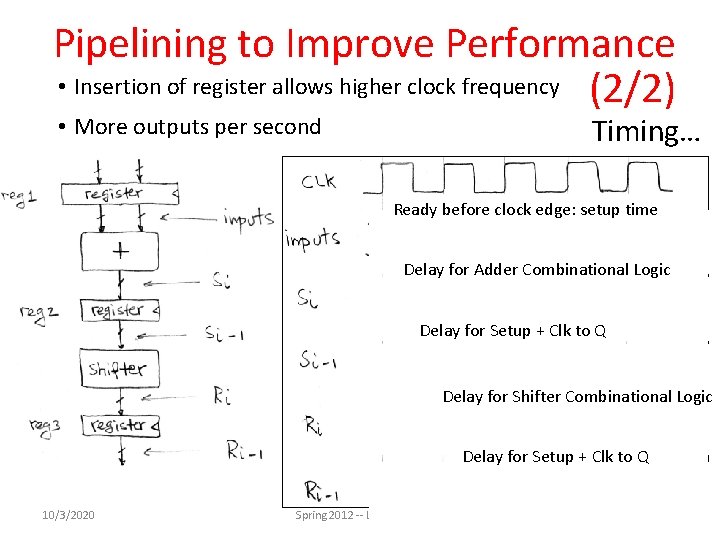
Pipelining to Improve Performance • Insertion of register allows higher clock frequency (2/2) Timing… • More outputs per second Ready before clock edge: setup time Delay for Adder Combinational Logic Delay for Setup + Clk to Q Delay for Shifter Combinational Logic Delay for Setup + Clk to Q 10/3/2020 Spring 2012 -- Lecture #18 19

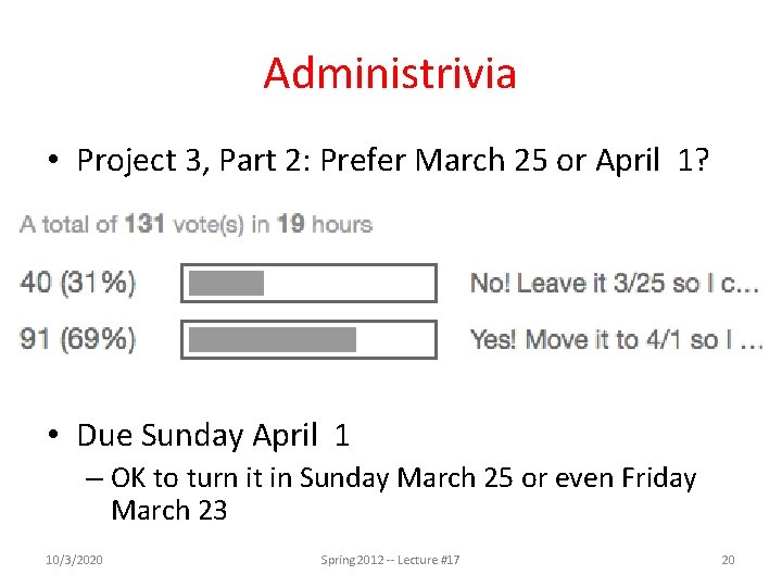
Administrivia • Project 3, Part 2: Prefer March 25 or April 1? • Due Sunday April 1 – OK to turn it in Sunday March 25 or even Friday March 23 10/3/2020 Spring 2012 -- Lecture #17 20

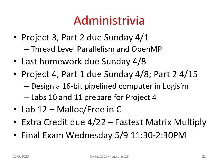
Administrivia • Project 3, Part 2 due Sunday 4/1 – Thread Level Parallelism and Open. MP • Last homework due Sunday 4/8 • Project 4, Part 1 due Sunday 4/8; Part 2 4/15 – Design a 16 -bit pipelined computer in Logisim – Labs 10 and 11 prepare for Project 4 • Lab 12 – Malloc/Free in C • Extra Credit due 4/22 – Fastest Matrix Multiply • Final Exam Wednesday 5/9 11: 30 -2: 30 PM 10/3/2020 Spring 2012 -- Lecture #18 21

Getting to Know Your Prof 1 son wanted to ride bike a “Century” 1 son wanted to Sprint Triathlon • Swim 0. 5 miles (0. 75 km) • Ride bike 12. 5 miles (20 km) • Run 3. 1 miles (5 km) • 102. 3 miles in 7: 04 • 10/3/2020 Avg 15 MPH, Max 38 Spring MPH 2012 -- Lecture #18 22

Agenda • • State Elements Administrivia Finite State Machines Introduction to Logisim Multiplexer ALU Design Summary 10/3/2020 Spring 2012 -- Lecture #18 23

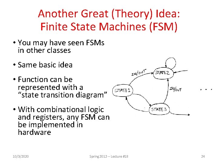
Another Great (Theory) Idea: Finite State Machines (FSM) • You may have seen FSMs in other classes • Same basic idea • Function can be represented with a “state transition diagram” • With combinational logic and registers, any FSM can be implemented in hardware 10/3/2020 Spring 2012 -- Lecture #18 24

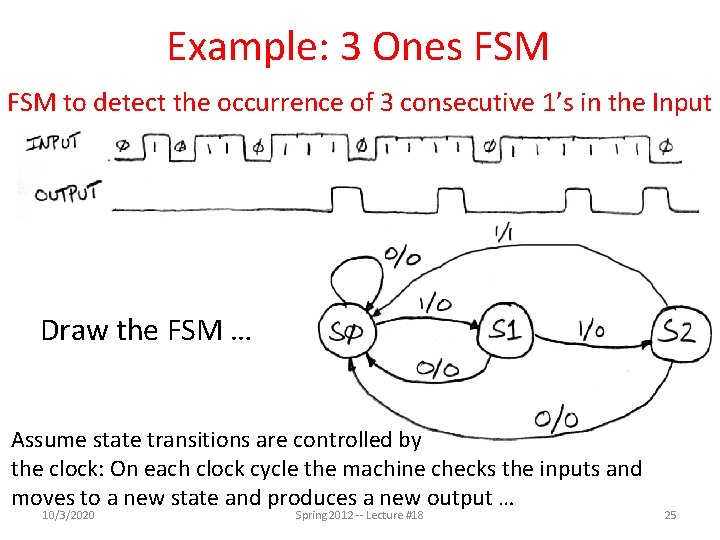
Example: 3 Ones FSM to detect the occurrence of 3 consecutive 1’s in the Input Draw the FSM … Assume state transitions are controlled by the clock: On each clock cycle the machine checks the inputs and moves to a new state and produces a new output … 10/3/2020 Spring 2012 -- Lecture #18 25

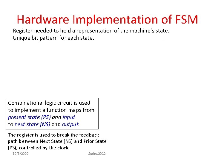
Hardware Implementation of FSM Register needed to hold a representation of the machine’s state. Unique bit pattern for each state. + Combinational logic circuit is used to implement a function maps from present state (PS) and input to next state (NS) and output. = The register is used to break the feedback path between Next State (NS) and Prior State (PS), controlled by the clock 10/3/2020 Spring 2012 -- Lecture #18 26

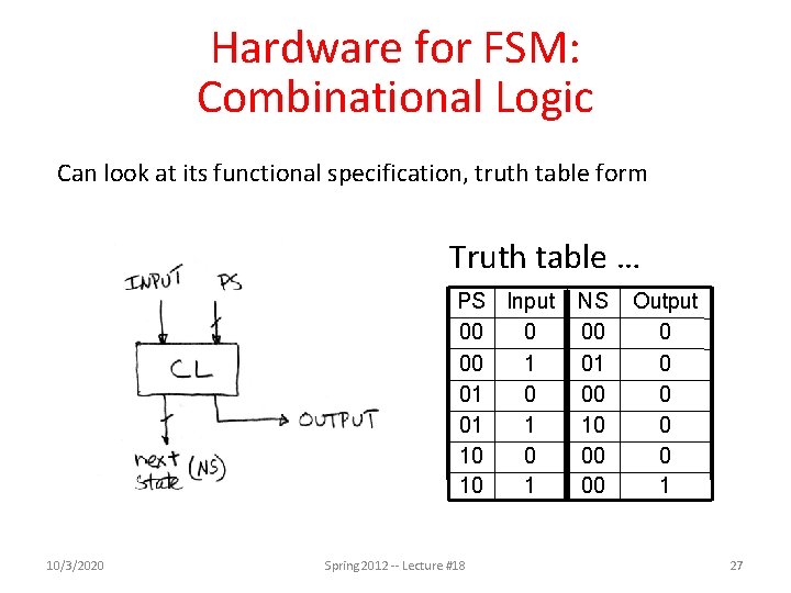
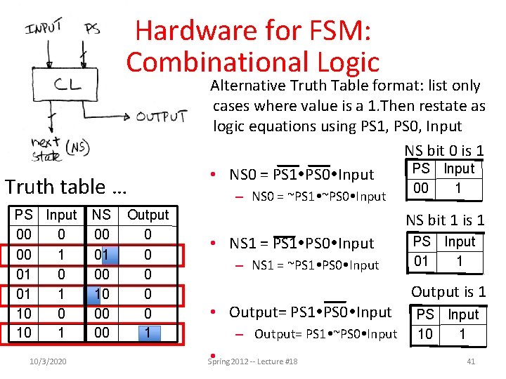
Hardware for FSM: Combinational Logic Can look at its functional specification, truth table form Truth table … PS Input 00 0 00 1 01 0 01 1 10 0 10 1 10/3/2020 Spring 2012 -- Lecture #18 NS 00 01 00 10 00 00 Output 0 0 0 1 27

Agenda • • State Elements Administrivia Finite State Machines Introduction to Logisim Multiplexer ALU Design Summary 10/3/2020 Spring 2012 -- Lecture #18 28

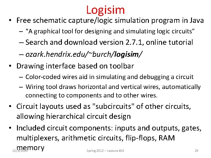
Logisim • Free schematic capture/logic simulation program in Java – “A graphical tool for designing and simulating logic circuits” – Search and download version 2. 7. 1, online tutorial – ozark. hendrix. edu/~burch/logisim/ • Drawing interface based on toolbar – Color-coded wires aid in simulating and debugging a circuit – Wiring tool draws horizontal and vertical wires, automatically connecting to components and to other wires. • Circuit layouts used as "subcircuits" of other circuits, allowing hierarchical circuit design • Included circuit components: inputs and outputs, gates, multiplexers, arithmetic circuits, flip-flops, RAM memory 10/3/2020 Spring 2012 -- Lecture #18 29

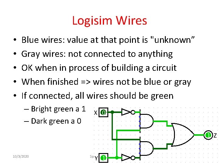
Logisim Wires • • • Blue wires: value at that point is "unknown” Gray wires: not connected to anything OK when in process of building a circuit When finished => wires not be blue or gray If connected, all wires should be green – Bright green a 1 – Dark green a 0 10/3/2020 Spring 2012 -- Lecture #18 30

Common Mistakes in Logisim • Connecting wires together • Using input for output • Connecting to edge without connecting to actual input – Unexpected direction of input 10/3/2020 Spring 2012 -- Lecture #18 31

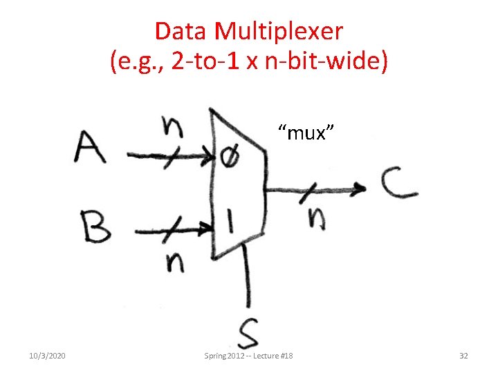
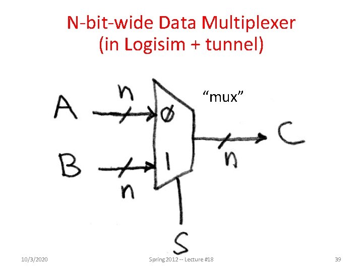
Data Multiplexer (e. g. , 2 -to-1 x n-bit-wide) “mux” 10/3/2020 Spring 2012 -- Lecture #18 32

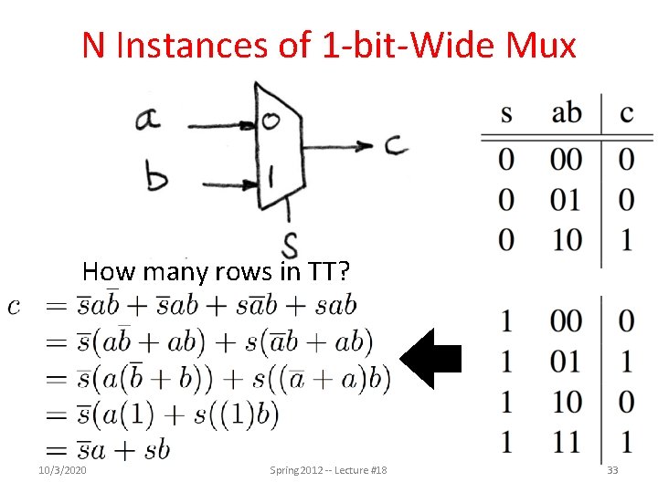
N Instances of 1 -bit-Wide Mux How many rows in TT? 10/3/2020 Spring 2012 -- Lecture #18 33

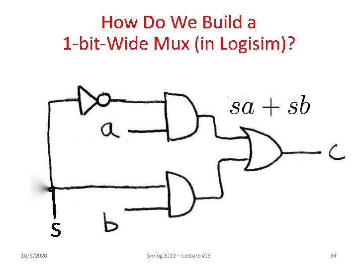
How Do We Build a 1 -bit-Wide Mux (in Logisim)? s 10/3/2020 Spring 2012 -- Lecture #18 34

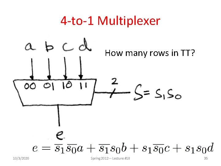
4 -to-1 Multiplexer How many rows in TT? 10/3/2020 Spring 2012 -- Lecture #18 35

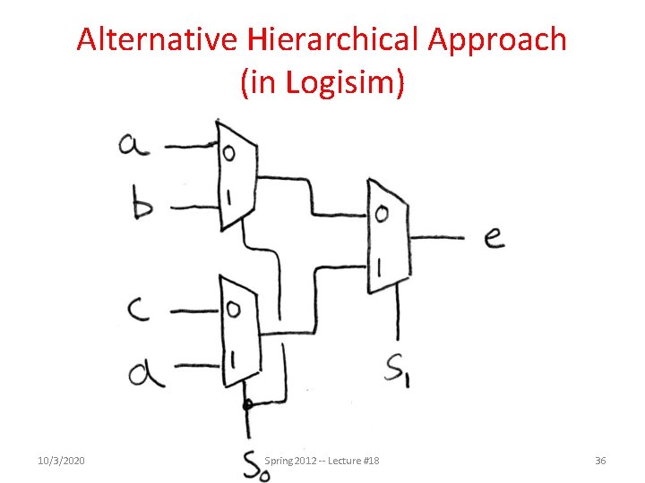
Alternative Hierarchical Approach (in Logisim) 10/3/2020 Spring 2012 -- Lecture #18 36

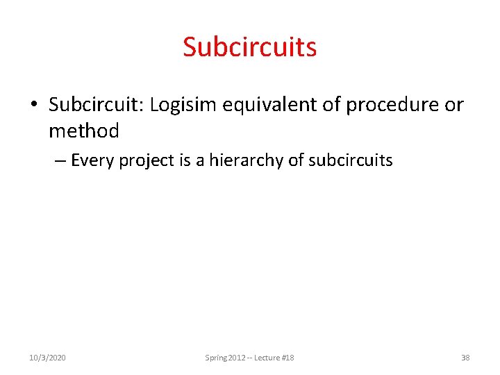
Subcircuits • Subcircuit: Logisim equivalent of procedure or method – Every project is a hierarchy of subcircuits 10/3/2020 Spring 2012 -- Lecture #18 38

N-bit-wide Data Multiplexer (in Logisim + tunnel) “mux” 10/3/2020 Spring 2012 -- Lecture #18 39

Hardware for FSM: Combinational Logic Can look at its functional specification, truth table form Truth table … PS Input 00 0 00 1 01 0 01 1 10 0 10 1 10/3/2020 Spring 2012 -- Lecture #18 NS 00 01 00 10 00 00 Output 0 0 0 1 40

Hardware for FSM: Combinational Logic Truth table … PS Input 00 0 00 1 01 0 01 1 10 0 10 1 10/3/2020 NS 00 01 00 10 00 00 Output 0 0 0 1 Alternative Truth Table format: list only cases where value is a 1. Then restate as logic equations using PS 1, PS 0, Input NS bit 0 is 1 PS Input • NS 0 = PS 1 PS 0 Input – NS 0 = ~PS 1 ~PS 0 Input 00 1 NS bit 1 is 1 • NS 1 = PS 1 PS 0 Input – NS 1 = ~PS 1 PS 0 Input • Output= PS 1 PS 0 Input – Output= PS 1 ~PS 0 Input • Spring 2012 -- Lecture #18 PS Input 01 1 Output is 1 PS Input 10 1 41

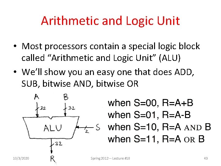
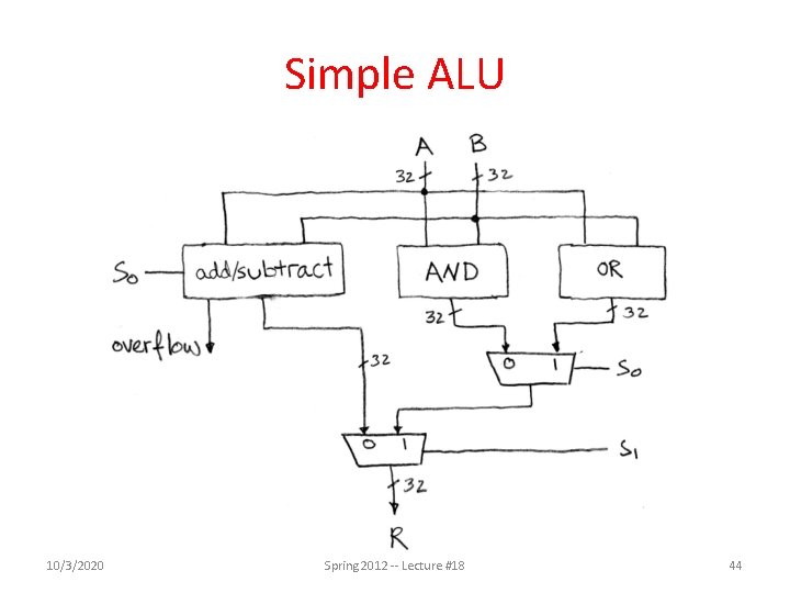
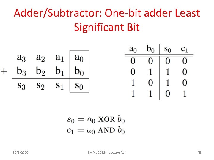
Arithmetic and Logic Unit • Most processors contain a special logic block called “Arithmetic and Logic Unit” (ALU) • We’ll show you an easy one that does ADD, SUB, bitwise AND, bitwise OR 10/3/2020 Spring 2012 -- Lecture #18 43

Simple ALU 10/3/2020 Spring 2012 -- Lecture #18 44

Adder/Subtractor: One-bit adder Least Significant Bit 10/3/2020 Spring 2012 -- Lecture #18 45

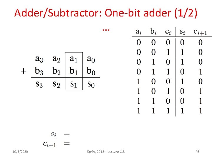
Adder/Subtractor: One-bit adder (1/2) … 10/3/2020 Spring 2012 -- Lecture #18 46

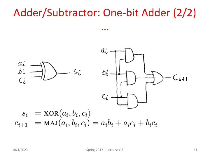
Adder/Subtractor: One-bit Adder (2/2) … 10/3/2020 Spring 2012 -- Lecture #18 47

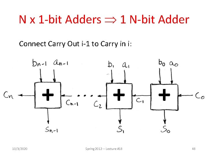
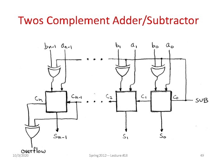
N x 1 -bit Adders 1 N-bit Adder Connect Carry Out i-1 to Carry in i: b 0 + 10/3/2020 + Spring 2012 -- Lecture #18 + 48

Twos Complement Adder/Subtractor 10/3/2020 Spring 2012 -- Lecture #18 49

Critical Path • When setting clock period in synchronous systems, must allow for worst case • Path through combinational logic that is worst case called “critical path” – Can be estimated by number of “gate delays”: Number of gates must go through in worst case • Idea: Doesn’t matter if speedup other paths if don’t improve the critical path • What might critical path of ALU? 10/3/2020 Spring 2012 -- Lecture #18 50

Summary • Hardware systems made from Stateless Combinational Logic and Stateful “Memory” Logic (Registers) • Clocks tell us when D-flip-flops change – Setup and Hold times important • We pipeline long-delay CL for faster clock cycle – Split up the critical path • Finite State Machines extremely useful • Use muxes to select among input – S input bits selects 2 S inputs – Each input can be n-bits wide, indep of S • Can implement muxes hierarchically • Can implement FSM with register + logic 10/3/2020 Spring 2012 -- Lecture #18 51