CS 152 Computer Architecture and Engineering Lecture 7
![3 b: Add & Subtract ° R[rd] < R[rs] op R[rt] Example: add. U 3 b: Add & Subtract ° R[rd] < R[rs] op R[rt] Example: add. U](https://slidetodoc.com/presentation_image_h2/b738b76398167734016cafb091a3539b/image-36.jpg)
![3 c: Logical Operations with Immediate ° R[rt] < R[rs] op Zero. Ext[imm 16] 3 c: Logical Operations with Immediate ° R[rt] < R[rs] op Zero. Ext[imm 16]](https://slidetodoc.com/presentation_image_h2/b738b76398167734016cafb091a3539b/image-38.jpg)
![3 d: Load Operations ° R[rt] < Mem[R[rs] + Sign. Ext[imm 16]] 31 26 3 d: Load Operations ° R[rt] < Mem[R[rs] + Sign. Ext[imm 16]] 31 26](https://slidetodoc.com/presentation_image_h2/b738b76398167734016cafb091a3539b/image-39.jpg)
![3 e: Store Operations ° Mem[ R[rs] + Sign. Ext[imm 16] < R[rt] ] 3 e: Store Operations ° Mem[ R[rs] + Sign. Ext[imm 16] < R[rt] ]](https://slidetodoc.com/presentation_image_h2/b738b76398167734016cafb091a3539b/image-40.jpg)
- Slides: 47

CS 152 Computer Architecture and Engineering Lecture 7 Designing a Single Cycle Datapath February 8, 2001 John Kubiatowicz (http. cs. berkeley. edu/~kubitron) lecture slides: http: //www inst. eecs. berkeley. edu/~cs 152/ 2/8/01 ©UCB Spring 2001 CS 152 / Kubiatowicz Lec 7. 1

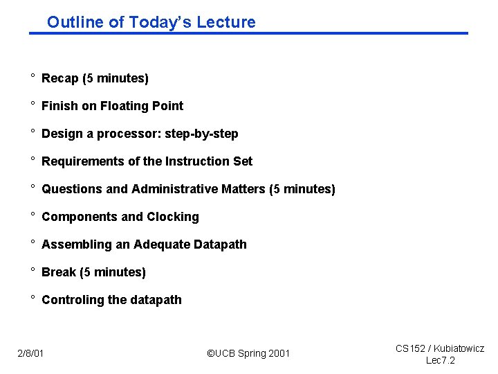
Outline of Today’s Lecture ° Recap (5 minutes) ° Finish on Floating Point ° Design a processor: step by step ° Requirements of the Instruction Set ° Questions and Administrative Matters (5 minutes) ° Components and Clocking ° Assembling an Adequate Datapath ° Break (5 minutes) ° Controling the datapath 2/8/01 ©UCB Spring 2001 CS 152 / Kubiatowicz Lec 7. 2

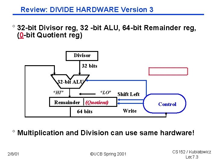
Review: DIVIDE HARDWARE Version 3 ° 32 bit Divisor reg, 32 bit ALU, 64 bit Remainder reg, (0 bit Quotient reg) Divisor 32 bits 32 -bit ALU “HI” “LO” Shift Left Remainder (Quotient) 64 bits Control Write ° Multiplication and Division can use same hardware! 2/8/01 ©UCB Spring 2001 CS 152 / Kubiatowicz Lec 7. 3

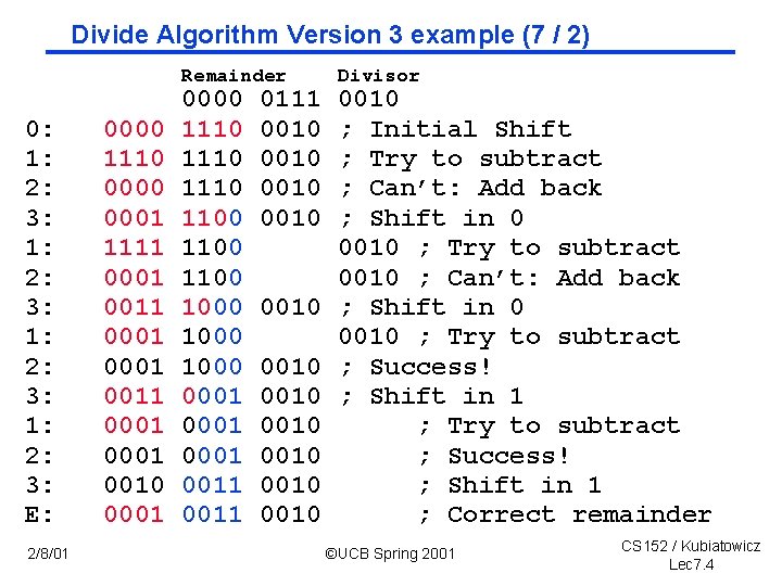
Divide Algorithm Version 3 example (7 / 2) Remainder 0: 1: 2: 3: E: 2/8/01 0000 1110 0001 1111 0001 0011 0001 0010 0001 0000 1110 1100 1000 0001 0011 0111 0010 0010 0010 Divisor 0010 ; Initial Shift ; Try to subtract ; Can’t: Add back ; Shift in 0 0010 ; Try to subtract 0010 ; Can’t: Add back ; Shift in 0 0010 ; Try to subtract ; Success! ; Shift in 1 ; Correct remainder ©UCB Spring 2001 CS 152 / Kubiatowicz Lec 7. 4

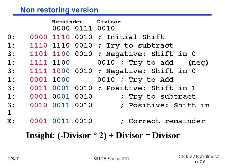
Non restoring version Remainder 0: 1: 3: 1 E: 0000 1110 1101 1111 0001 0010 0000 1110 1100 1000 0001 0011 0111 0010 0010 0001 0010 Divisor 0010 ; Initial Shift ; Try to subtract ; Negative: Shift in 0 0010 ; Try to add (neg) ; Negative: Shift in 0 0010 ; Try to Add ; Positive: Shift in 1 ; Try to subtract ; Positive: Shift in ; Correct remainder Insight: (-Divisor * 2) + Divisor = Divisor 2/8/01 ©UCB Spring 2001 CS 152 / Kubiatowicz Lec 7. 5

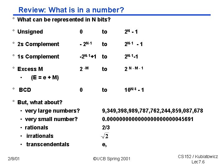
Review: What is in a number? ° What can be represented in N bits? ° Unsigned 0 to 2 N 1 ° 2 s Complement 2 N 1 to 2 N 1 1 ° 1 s Complement 2 N 1+1 to 2 N 1 1 ° Excess M • (E = e + M) 2 M to 2 N M 1 ° BCD 0 to 10 N/4 1 ° But, what about? • very large numbers? • very small number? • rationals • irrationals • transcendentals 2/8/01 9, 349, 398, 989, 787, 762, 244, 859, 087, 678 0. 00000000000045691 2/3 e, ©UCB Spring 2001 CS 152 / Kubiatowicz Lec 7. 6

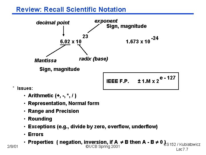
Review: Recall Scientific Notation exponent Sign, magnitude decimal point 6. 02 x 10 Mantissa 23 1. 673 x 10 24 radix (base) Sign, magnitude IEEE F. P. ± 1. M x 2 e 127 ° Issues: 2/8/01 • • Arithmetic (+, , *, / ) Representation, Normal form Range and Precision Rounding Exceptions (e. g. , divide by zero, overflow, underflow) Errors Properties ( negation, inversion, if A B then A B 0 CS 152 ) / Kubiatowicz ©UCB Spring 2001 Lec 7. 7

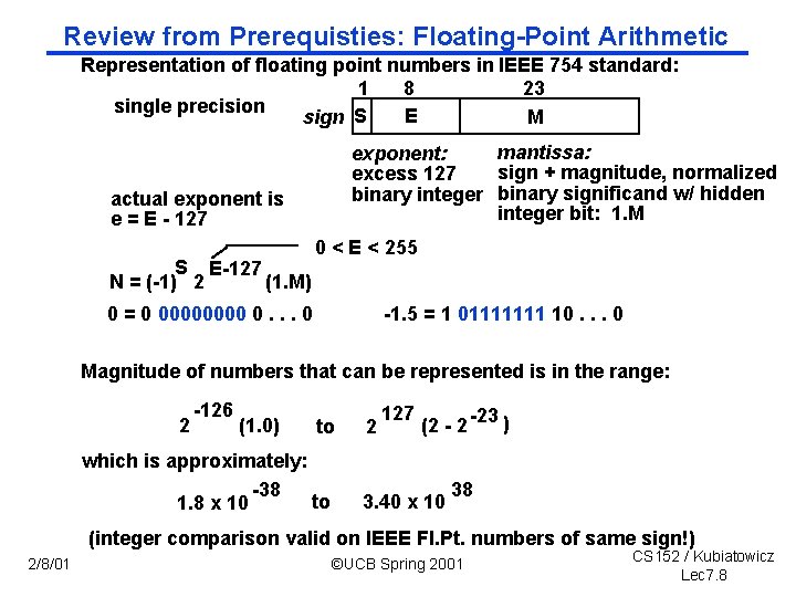
Review from Prerequisties: Floating Point Arithmetic Representation of floating point numbers in IEEE 754 standard: 1 8 23 single precision E sign S M mantissa: exponent: sign + magnitude, normalized excess 127 binary integer binary significand w/ hidden integer bit: 1. M actual exponent is e = E 127 S E 127 N = ( 1) 2 (1. M) 0 < E < 255 0 = 0 0000 0. . . 0 1. 5 = 1 01111111 10. . . 0 Magnitude of numbers that can be represented is in the range: 2 126 (1. 0) to which is approximately: 38 to 1. 8 x 10 2 127 (2 2 23 ) 3. 40 x 10 38 (integer comparison valid on IEEE Fl. Pt. numbers of same sign!) 2/8/01 ©UCB Spring 2001 CS 152 / Kubiatowicz Lec 7. 8

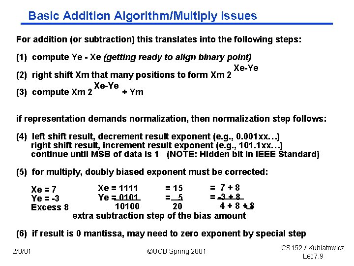
Basic Addition Algorithm/Multiply issues For addition (or subtraction) this translates into the following steps: (1) compute Ye Xe (getting ready to align binary point) Xe Ye (2) right shift Xm that many positions to form Xm 2 Xe Ye (3) compute Xm 2 + Ym if representation demands normalization, then normalization step follows: (4) left shift result, decrement result exponent (e. g. , 0. 001 xx…) right shift result, increment result exponent (e. g. , 101. 1 xx…) continue until MSB of data is 1 (NOTE: Hidden bit in IEEE Standard) (5) for multiply, doubly biased exponent must be corrected: Xe = 7 Ye = 3 Excess 8 = 7+8 Xe = 1111 = 15 = 3 + 8 Ye = 0101 = 5 4+8+8 10100 20 extra subtraction step of the bias amount (6) if result is 0 mantissa, may need to zero exponent by special step 2/8/01 ©UCB Spring 2001 CS 152 / Kubiatowicz Lec 7. 9

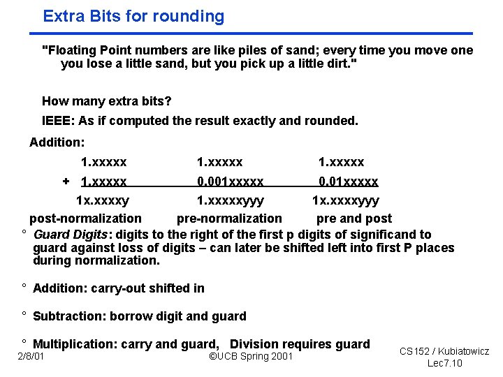
Extra Bits for rounding "Floating Point numbers are like piles of sand; every time you move one you lose a little sand, but you pick up a little dirt. " How many extra bits? IEEE: As if computed the result exactly and rounded. Addition: 1. xxxxx + 1. xxxxx 0. 001 xxxxx 0. 01 xxxxx 1 x. xxxxy 1. xxxxxyyy 1 x. xxxxyyy post normalization pre and post ° Guard Digits: digits to the right of the first p digits of significand to guard against loss of digits – can later be shifted left into first P places during normalization. ° Addition: carry out shifted in ° Subtraction: borrow digit and guard ° Multiplication: carry and guard, Division requires guard 2/8/01 ©UCB Spring 2001 CS 152 / Kubiatowicz Lec 7. 10

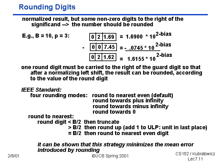
Rounding Digits normalized result, but some non zero digits to the right of the significand > the number should be rounded = 1. 6900 * 102 bias 0 0 7. 45 = . 0745 * 10 2 bias 0 2 1. 62 = 1. 6155 * 10 2 bias one round digit must be carried to the right of the guard digit so that after a normalizing left shift, the result can be rounded, according to the value of the round digit E. g. , B = 10, p = 3: 0 2 1. 69 IEEE Standard: four rounding modes: round to nearest even (default) round towards plus infinity round towards minus infinity round towards 0 round to nearest: round digit < B/2 then truncate > B/2 then round up (add 1 to ULP: unit in last place) = B/2 then round to nearest even digit it can be shown that this strategy minimizes the mean error introduced by rounding 2/8/01 ©UCB Spring 2001 CS 152 / Kubiatowicz Lec 7. 11

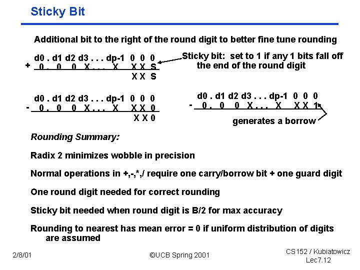
Sticky Bit Additional bit to the right of the round digit to better fine tune rounding d 0. d 1 d 2 d 3. . . dp 1 0 0 0 + 0. 0 0 X. . . X XX S d 0. d 1 d 2 d 3. . . dp 1 0 0 0 0. 0 0 X. . . X XX 0 Sticky bit: set to 1 if any 1 bits fall off the end of the round digit d 0. d 1 d 2 d 3. . . dp 1 0 0 0 0. 0 0 X. . . X XX 1 generates a borrow Rounding Summary: Radix 2 minimizes wobble in precision Normal operations in +, , *, / require one carry/borrow bit + one guard digit One round digit needed for correct rounding Sticky bit needed when round digit is B/2 for max accuracy Rounding to nearest has mean error = 0 if uniform distribution of digits are assumed 2/8/01 ©UCB Spring 2001 CS 152 / Kubiatowicz Lec 7. 12

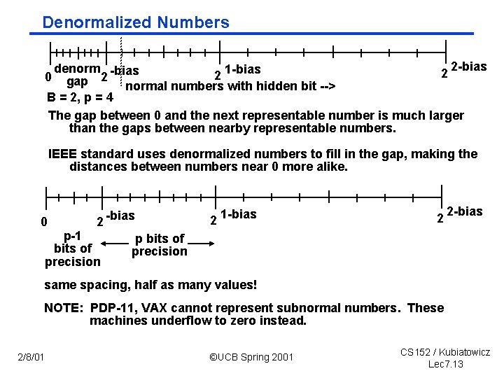
Denormalized Numbers 2 bias denorm bias 1 bias 2 2 2 gap normal numbers with hidden bit > B = 2, p = 4 The gap between 0 and the next representable number is much larger than the gaps between nearby representable numbers. 0 IEEE standard uses denormalized numbers to fill in the gap, making the distances between numbers near 0 more alike. 0 2 bias p 1 bits of precision 2 1 bias 2 2 bias p bits of precision same spacing, half as many values! NOTE: PDP 11, VAX cannot represent subnormal numbers. These machines underflow to zero instead. 2/8/01 ©UCB Spring 2001 CS 152 / Kubiatowicz Lec 7. 13

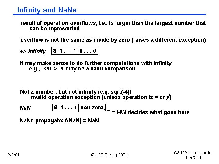
Infinity and Na. Ns result of operation overflows, i. e. , is larger than the largest number that can be represented overflow is not the same as divide by zero (raises a different exception) +/- infinity S 1. . . 1 0. . . 0 It may make sense to do further computations with infinity e. g. , X/0 > Y may be a valid comparison Not a number, but not infinity (e. q. sqrt( 4)) invalid operation exception (unless operation is = or =) Na. N S 1. . . 1 non zero HW decides what goes here Na. Ns propagate: f(Na. N) = Na. N 2/8/01 ©UCB Spring 2001 CS 152 / Kubiatowicz Lec 7. 14

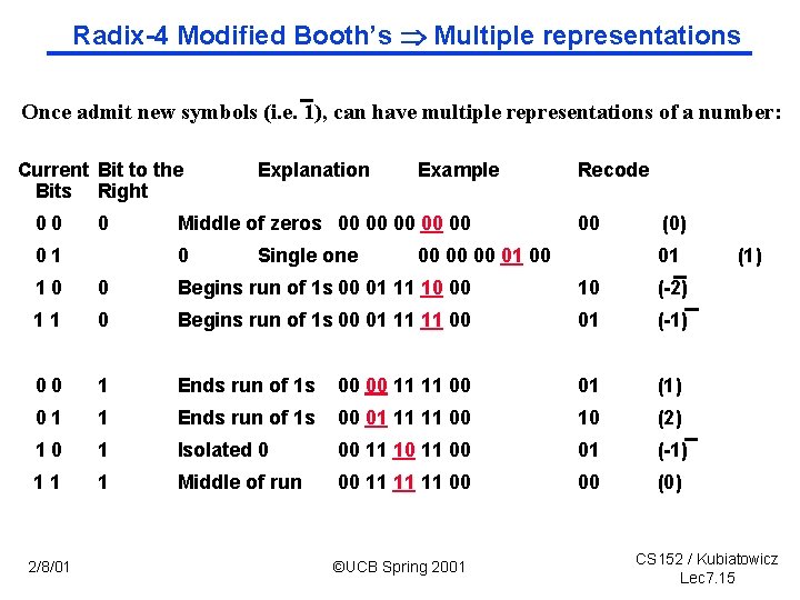
Radix 4 Modified Booth’s Multiple representations Once admit new symbols (i. e. 1), can have multiple representations of a number: Current Bit to the Bits Right 00 0 01 Explanation Example Middle of zeros 00 00 00 0 Single one Recode 00 00 01 00 (0) 01 10 0 Begins run of 1 s 00 01 11 10 00 10 ( 2) 11 0 Begins run of 1 s 00 01 11 11 00 01 ( 1) 00 1 Ends run of 1 s 00 00 11 11 00 01 (1) 01 1 Ends run of 1 s 00 01 11 11 00 10 (2) 10 1 Isolated 0 00 11 10 11 00 01 ( 1) 11 1 Middle of run 00 11 11 11 00 00 (0) 2/8/01 ©UCB Spring 2001 (1) CS 152 / Kubiatowicz Lec 7. 15

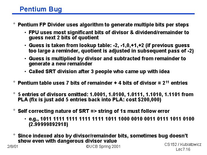
Pentium Bug ° Pentium FP Divider uses algorithm to generate multiple bits per steps • FPU uses most significant bits of divisor & dividend/remainder to guess next 2 bits of quotient • Guess is taken from lookup table: 2, 1, 0, +1, +2 (if previous guess too large a reminder, quotient is adjusted in subsequent pass of 2) • Guess is multiplied by divisor and subtracted from remainder to generate a new remainder • Called SRT division after 3 people who came up with idea ° Pentium table uses 7 bits of remainder + 4 bits of divisor = 2 11 entries ° 5 entries of divisors omitted: 1. 0001, 1. 0100, 1. 0111, 1. 1010, 1. 1101 from PLA (fix is just add 5 entries back into PLA: cost $200, 000) ° Self correcting nature of SRT => string of 1 s must follow error • e. g. , 1011 1111 1000 0011 0111 1011 0100 (2. 99999892918) ° Since indexed also by divisor/remainder bits, sometimes bug doesn’t show even with dangerous divisor value 2/8/01 ©UCB Spring 2001 CS 152 / Kubiatowicz Lec 7. 16

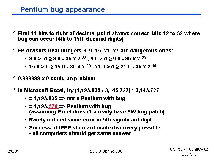
Pentium bug appearance ° First 11 bits to right of decimal point always correct: bits 12 to 52 where bug can occur (4 th to 15 th decimal digits) ° FP divisors near integers 3, 9, 15, 21, 27 are dangerous ones: • 3. 0 > d 3. 0 36 x 2– 22 , 9. 0 > d 9. 0 36 x 2– 20 • 15. 0 > d 15. 0 36 x 2– 20 , 21. 0 > d 21. 0 36 x 2– 19 ° 0. 333333 x 9 could be problem ° In Microsoft Excel, try (4, 195, 835 / 3, 145, 727) * 3, 145, 727 • = 4, 195, 835 => not a Pentium with bug • = 4, 195, 579 => Pentium with bug (assuming Excel doesn’t already have SW bug patch) • Rarely noticed since error in 5 th significant digit • Success of IEEE standard made discovery possible: all computers should get same answer 2/8/01 ©UCB Spring 2001 CS 152 / Kubiatowicz Lec 7. 17

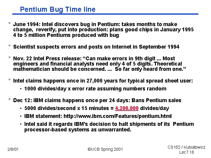
Pentium Bug Time line ° June 1994: Intel discovers bug in Pentium: takes months to make change, reverify, put into production: plans good chips in January 1995 4 to 5 million Pentiums produced with bug ° Scientist suspects errors and posts on Internet in September 1994 ° Nov. 22 Intel Press release: “Can make errors in 9 th digit. . . Most engineers and financial analysts need only 4 of 5 digits. Theoretical mathematician should be concerned. . So far only heard from one. ” ° Intel claims happens once in 27, 000 years for typical spread sheet user: • 1000 divides/day x error rate assuming numbers random ° Dec 12: IBM claims happens once per 24 days: Bans Pentium sales • 5000 divides/second x 15 minutes = 4, 200, 000 divides/day • IBM statement: http: //www. ibm. com/Features/pentium. html • Intel said it regards IBM's decision to halt shipments of its Pentium processor based systems as unwarranted. 2/8/01 ©UCB Spring 2001 CS 152 / Kubiatowicz Lec 7. 18

Pentium conclusion: Dec. 21, 1994 $500 M write off “To owners of Pentium processor based computers and the PC community: We at Intel wish to sincerely apologize for our handling of the recently publicized Pentium processor flaw. The Intel Inside symbol means that your computer has a microprocessor second to none in quality and performance. Thousands of Intel employees work very hard to ensure that this is true. But no microprocessor is ever perfect. What Intel continues to believe is technically an extremely minor problem has taken on a life of its own. Although Intel firmly stands behind the quality of the current version of the Pentium processor, we recognize that many users have concerns. We want to resolve these concerns. Intel will exchange the current version of the Pentium processor for an updated version, in which this floating point divide flaw is corrected, for any owner who requests it, free of charge anytime during the life of their computer. Just call 1 800 628 8686. ” Sincerely, Andrew S. Grove President /CEO 2/8/01 Craig R. Barrett Executive Vice President &COO ©UCB Spring 2001 Gordon E. Moore Chairman of the Board CS 152 / Kubiatowicz Lec 7. 19

Questions and Administrative Matters (5 Minutes) ° Reading Assignment 5. 1 5. 4 ° Project teams choose next Wednesday: • Form four or five people project team. • We want you to learn to work in a big team. • Other project members must be in same section ° Make sure to look for assignments on Handouts page ° Midterm Thursday 3/1 in 277 Cory 5: 30 PM 8: 30 PM • you may bring one double sided page of notes • we’ll give you the opcode table from the book • review session Sunday before(? ) • previous midterms and solutions on line for review 2/8/01 ©UCB Spring 2001 CS 152 / Kubiatowicz Lec 7. 20

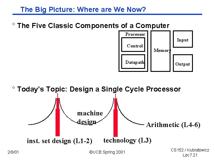
The Big Picture: Where are We Now? ° The Five Classic Components of a Computer Processor Input Control Memory Datapath Output ° Today’s Topic: Design a Single Cycle Processor machine design inst. set design (L 1 -2) 2/8/01 Arithmetic (L 4 -6) technology (L 3) ©UCB Spring 2001 CS 152 / Kubiatowicz Lec 7. 21

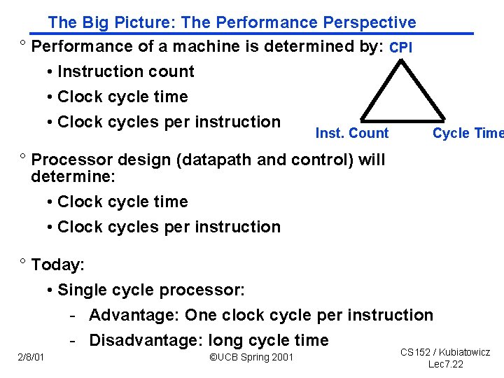
The Big Picture: The Performance Perspective ° Performance of a machine is determined by: CPI • Instruction count • Clock cycle time • Clock cycles per instruction Inst. Count Cycle Time ° Processor design (datapath and control) will determine: • Clock cycle time • Clock cycles per instruction ° Today: • Single cycle processor: - Advantage: One clock cycle per instruction - Disadvantage: long cycle time 2/8/01 ©UCB Spring 2001 CS 152 / Kubiatowicz Lec 7. 22

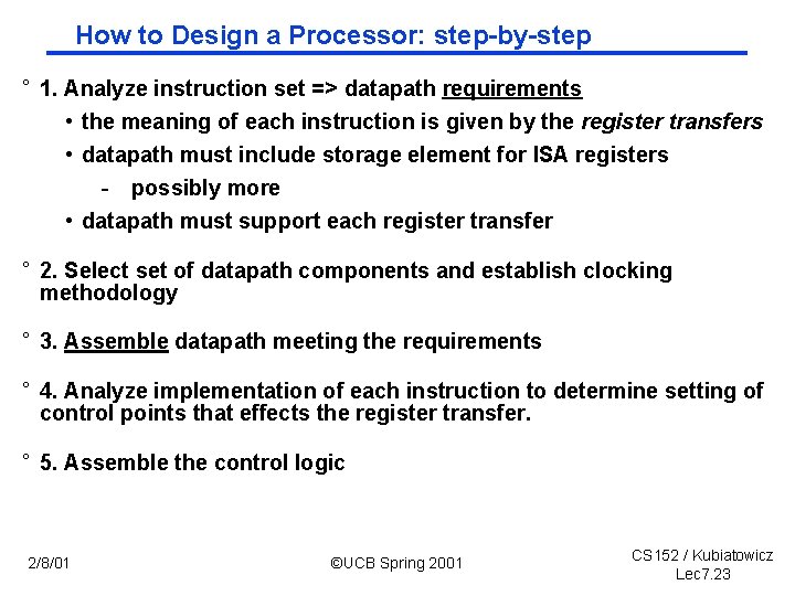
How to Design a Processor: step by step ° 1. Analyze instruction set => datapath requirements • the meaning of each instruction is given by the register transfers • datapath must include storage element for ISA registers - possibly more • datapath must support each register transfer ° 2. Select set of datapath components and establish clocking methodology ° 3. Assemble datapath meeting the requirements ° 4. Analyze implementation of each instruction to determine setting of control points that effects the register transfer. ° 5. Assemble the control logic 2/8/01 ©UCB Spring 2001 CS 152 / Kubiatowicz Lec 7. 23

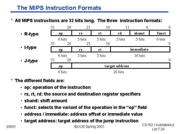
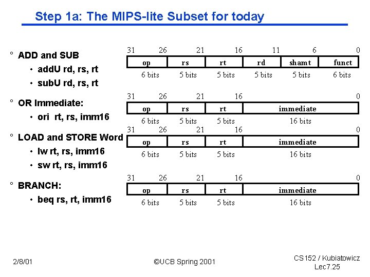
The MIPS Instruction Formats ° All MIPS instructions are 32 bits long. The three instruction formats: 31 26 op • R type rs 6 bits • I type • J type 31 21 op 6 bits 31 rt 5 bits 26 16 5 bits 21 rs 5 bits 11 6 rd shamt funct 5 bits 6 bits 16 rt 5 bits 0 immediate 16 bits 26 0 op 6 bits target address 26 bits ° The different fields are: • op: operation of the instruction • rs, rt, rd: the source and destination register specifiers • shamt: shift amount • funct: selects the variant of the operation in the “op” field • address / immediate: address offset or immediate value • target address: target address of the jump instruction 2/8/01 0 ©UCB Spring 2001 CS 152 / Kubiatowicz Lec 7. 24

Step 1 a: The MIPS lite Subset for today ° ADD and SUB • add. U rd, rs, rt • sub. U rd, rs, rt 31 26 op 6 bits rs 5 bits 16 rt 5 bits 26 21 16 op 6 bits 31 26 ° LOAD and STORE Word op rs 5 bits 21 rs rt 5 bits 16 rt 5 bits ° OR Immediate: • ori rt, rs, imm 16 31 21 • lw rt, rs, imm 16 • sw rt, rs, imm 16 ° BRANCH: • beq rs, rt, imm 16 2/8/01 6 bits 31 26 op 6 bits 21 rs 5 bits ©UCB Spring 2001 11 rd 5 bits 6 shamt 5 bits funct 6 bits 0 immediate 16 bits 16 rt 5 bits 0 0 immediate 16 bits CS 152 / Kubiatowicz Lec 7. 25

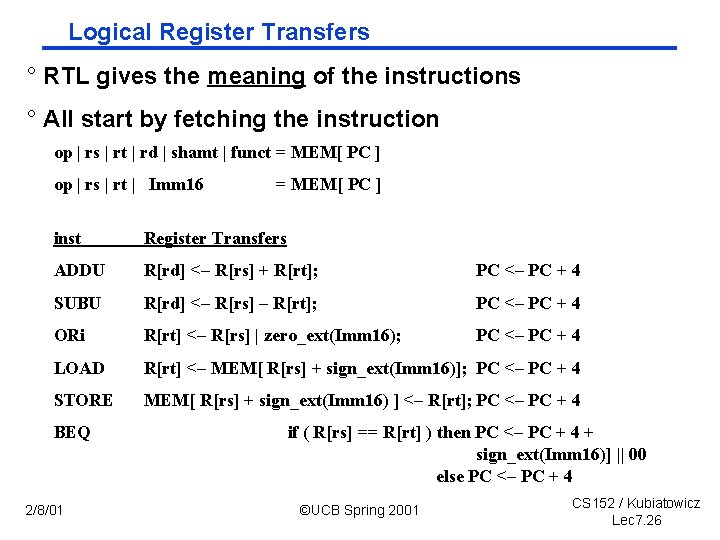
Logical Register Transfers ° RTL gives the meaning of the instructions ° All start by fetching the instruction op | rs | rt | rd | shamt | funct = MEM[ PC ] op | rs | rt | Imm 16 = MEM[ PC ] inst Register Transfers ADDU R[rd] <– R[rs] + R[rt]; PC <– PC + 4 SUBU R[rd] <– R[rs] – R[rt]; PC <– PC + 4 ORi R[rt] <– R[rs] | zero_ext(Imm 16); PC <– PC + 4 LOAD R[rt] <– MEM[ R[rs] + sign_ext(Imm 16)]; PC <– PC + 4 STORE MEM[ R[rs] + sign_ext(Imm 16) ] <– R[rt]; PC <– PC + 4 BEQ 2/8/01 if ( R[rs] == R[rt] ) then PC <– PC + 4 + sign_ext(Imm 16)] || 00 else PC <– PC + 4 ©UCB Spring 2001 CS 152 / Kubiatowicz Lec 7. 26

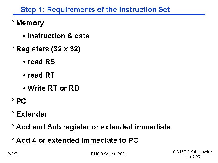
Step 1: Requirements of the Instruction Set ° Memory • instruction & data ° Registers (32 x 32) • read RS • read RT • Write RT or RD ° PC ° Extender ° Add and Sub register or extended immediate ° Add 4 or extended immediate to PC 2/8/01 ©UCB Spring 2001 CS 152 / Kubiatowicz Lec 7. 27

Step 2: Components of the Datapath ° Combinational Elements ° Storage Elements • Clocking methodology 2/8/01 ©UCB Spring 2001 CS 152 / Kubiatowicz Lec 7. 28

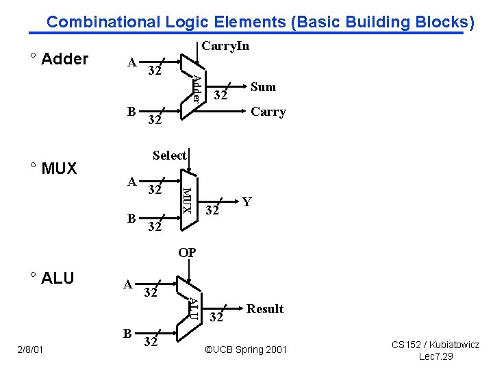
Combinational Logic Elements (Basic Building Blocks) ° Adder Carry. In A ° MUX Adder B 32 32 Sum Carry 32 Select B 32 MUX A 32 Y 32 OP ° ALU A 2/8/01 32 ALU B 32 32 Result ©UCB Spring 2001 CS 152 / Kubiatowicz Lec 7. 29

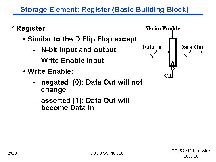
Storage Element: Register (Basic Building Block) Write Enable ° Register • Similar to the D Flip Flop except Data In Data Out - N bit input and output N N - Write Enable input • Write Enable: Clk - negated (0): Data Out will not change - asserted (1): Data Out will become Data In 2/8/01 ©UCB Spring 2001 CS 152 / Kubiatowicz Lec 7. 30

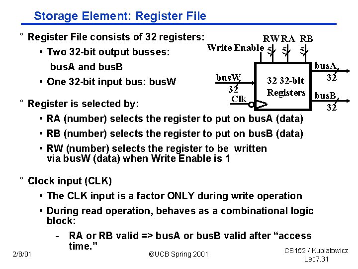
Storage Element: Register File ° Register File consists of 32 registers: RWRA RB Write Enable 5 5 5 • Two 32 bit output busses: bus. A and bus. B bus. W 32 32 32 -bit • One 32 bit input bus: bus. W 32 Registers bus. B Clk ° Register is selected by: 32 • RA (number) selects the register to put on bus. A (data) • RB (number) selects the register to put on bus. B (data) • RW (number) selects the register to be written via bus. W (data) when Write Enable is 1 ° Clock input (CLK) • The CLK input is a factor ONLY during write operation • During read operation, behaves as a combinational logic block: - RA or RB valid => bus. A or bus. B valid after “access time. ” CS 152 / Kubiatowicz 2/8/01 ©UCB Spring 2001 Lec 7. 31

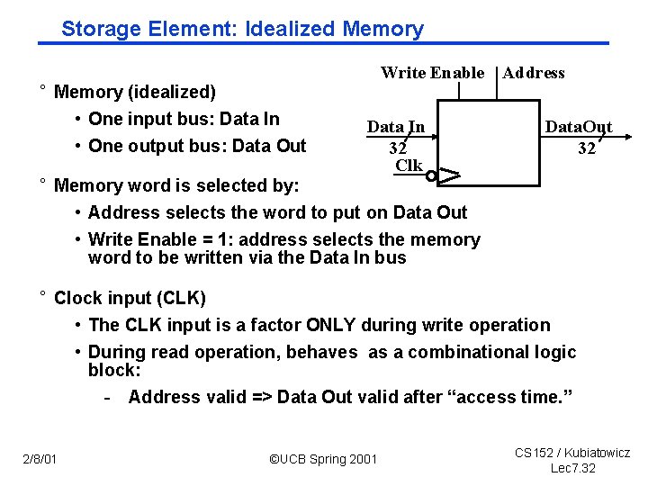
Storage Element: Idealized Memory ° Memory (idealized) • One input bus: Data In • One output bus: Data Out Write Enable Address Data In 32 Clk Data. Out 32 ° Memory word is selected by: • Address selects the word to put on Data Out • Write Enable = 1: address selects the memory word to be written via the Data In bus ° Clock input (CLK) • The CLK input is a factor ONLY during write operation • During read operation, behaves as a combinational logic block: - Address valid => Data Out valid after “access time. ” 2/8/01 ©UCB Spring 2001 CS 152 / Kubiatowicz Lec 7. 32

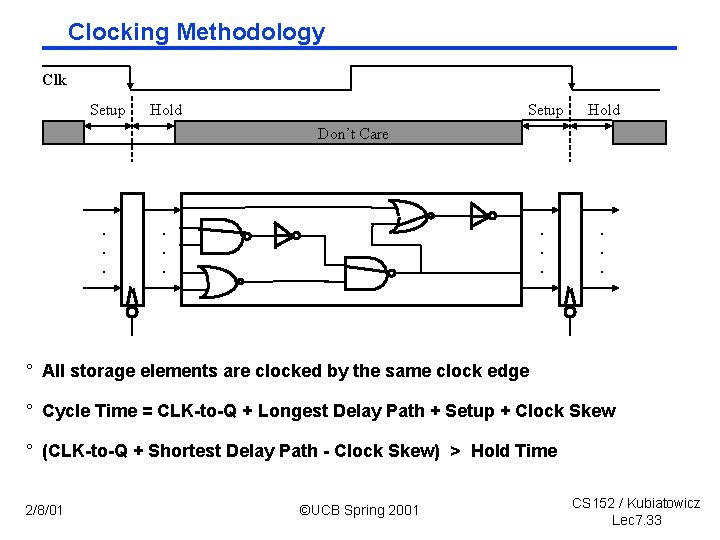
Clocking Methodology Clk Setup Hold . . . Don’t Care . . . ° All storage elements are clocked by the same clock edge ° Cycle Time = CLK to Q + Longest Delay Path + Setup + Clock Skew ° (CLK to Q + Shortest Delay Path Clock Skew) > Hold Time 2/8/01 ©UCB Spring 2001 CS 152 / Kubiatowicz Lec 7. 33

Step 3: Assemble Data. Path meeting our requirements ° Register Transfer Requirements Datapath Assembly ° Instruction Fetch ° Read Operands and Execute Operation 2/8/01 ©UCB Spring 2001 CS 152 / Kubiatowicz Lec 7. 34

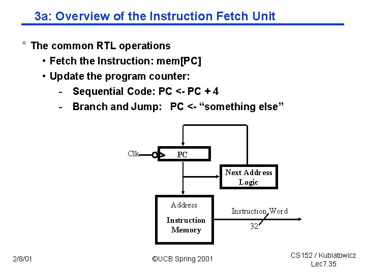
3 a: Overview of the Instruction Fetch Unit ° The common RTL operations • Fetch the Instruction: mem[PC] • Update the program counter: - Sequential Code: PC < PC + 4 - Branch and Jump: PC < “something else” Clk PC Next Address Logic Address Instruction Memory 2/8/01 ©UCB Spring 2001 Instruction Word 32 CS 152 / Kubiatowicz Lec 7. 35
![3 b Add Subtract Rrd Rrs op Rrt Example add U 3 b: Add & Subtract ° R[rd] < R[rs] op R[rt] Example: add. U](https://slidetodoc.com/presentation_image_h2/b738b76398167734016cafb091a3539b/image-36.jpg)
3 b: Add & Subtract ° R[rd] < R[rs] op R[rt] Example: add. U rd, rs, rt • Ra, Rb, and Rw come from instruction’s rs, rt, and rd fields • ALUctr and Reg. Wr: control logic after decoding the instruction 31 26 op 6 bits Reg. Wr 21 16 rs 5 bits rt 5 bits 32 32 -bit Registers 6 shamt 5 bits 0 funct 6 bits ALUctr bus. A 32 bus. B 32 ©UCB Spring 2001 ALU 2/8/01 rd 5 bits Rd Rs Rt 5 5 5 Rw Ra Rb bus. W 32 Clk 11 Result 32 CS 152 / Kubiatowicz Lec 7. 36

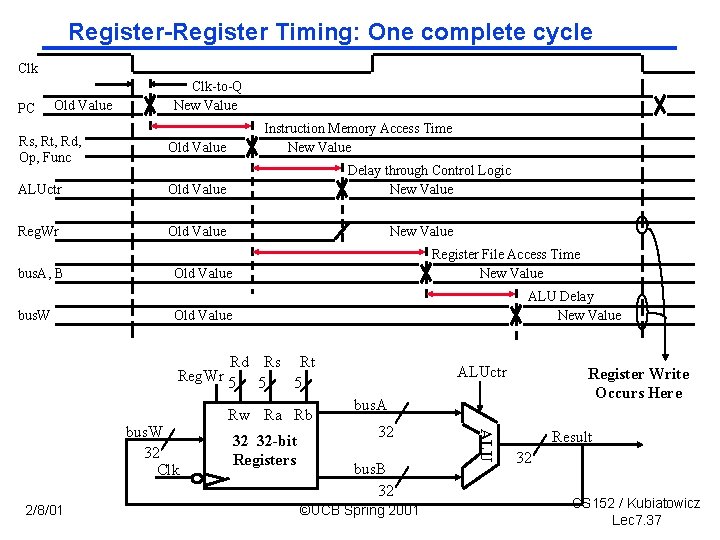
Register Timing: One complete cycle Clk PC Old Value Clk-to-Q New Value Rs, Rt, Rd, Op, Func Old Value ALUctr Old Value Reg. Wr Old Value bus. A, B bus. W Instruction Memory Access Time New Value Delay through Control Logic New Value Register File Access Time New Value Old Value ALU Delay New Value Old Value Rd Rs Rt Reg. Wr 5 5 5 2/8/01 32 32 -bit Registers Register Write Occurs Here bus. A 32 bus. B 32 ©UCB Spring 2001 ALU bus. W 32 Clk Rw Ra Rb ALUctr Result 32 CS 152 / Kubiatowicz Lec 7. 37
![3 c Logical Operations with Immediate Rrt Rrs op Zero Extimm 16 3 c: Logical Operations with Immediate ° R[rt] < R[rs] op Zero. Ext[imm 16]](https://slidetodoc.com/presentation_image_h2/b738b76398167734016cafb091a3539b/image-38.jpg)
3 c: Logical Operations with Immediate ° R[rt] < R[rs] op Zero. Ext[imm 16] ] 31 26 op 6 bits 21 rs 5 bits rt 5 bits 31 Reg. Dst Mux Rs Rt? 5 5 Rw Ra Rb 32 32 -bit Registers bus. A 32 bus. B 32 Result 32 Mux 16 ALUctr Zero. Ext imm 16 2/8/01 0 immediate 16 bits ALU 32 Clk 16 15 0 immediate 16 bits rd? 00000000 16 bits Rt Rd Reg. Wr 5 bus. W 11 16 32 ALUSrc ©UCB Spring 2001 CS 152 / Kubiatowicz Lec 7. 38
![3 d Load Operations Rrt MemRrs Sign Extimm 16 31 26 3 d: Load Operations ° R[rt] < Mem[R[rs] + Sign. Ext[imm 16]] 31 26](https://slidetodoc.com/presentation_image_h2/b738b76398167734016cafb091a3539b/image-39.jpg)
3 d: Load Operations ° R[rt] < Mem[R[rs] + Sign. Ext[imm 16]] 31 26 op 6 bits Rd Reg. Dst Mux Reg. Wr 5 32 Clk rt 5 bits 0 immediate 16 bits rd Rt Rs Rt? 5 5 Rw Ra Rb 32 32 -bit Registers bus. A W_Src 32 32 Ext. Op 32 Mem. Wr ? ? ALUSrc Data In 32 Clk ©UCB Spring 2001 Mux bus. B 32 Mux 16 ALUctr Extender imm 16 2/8/01 rs 5 bits rt, rs, imm 16 11 16 ALU bus. W 21 Example: lw Wr. En Adr Data Memory 32 CS 152 / Kubiatowicz Lec 7. 39
![3 e Store Operations Mem Rrs Sign Extimm 16 Rrt 3 e: Store Operations ° Mem[ R[rs] + Sign. Ext[imm 16] < R[rt] ]](https://slidetodoc.com/presentation_image_h2/b738b76398167734016cafb091a3539b/image-40.jpg)
3 e: Store Operations ° Mem[ R[rs] + Sign. Ext[imm 16] < R[rt] ] Example: sw 31 26 21 op Reg. Dst 16 rs 6 bits Rd Rt rt 5 bits 0 immediate 5 bits 16 bits ALUctr Mem. Wr W_Src Mux Reg. Wr 5 32 Clk 5 Rs 5 Rt Rw Ra Rb 32 32 -bit Registers 32 Ext. Op 32 Data In 32 Clk Wr. En Adr Data Memory Mux bus. B 32 Mux 16 32 Extender imm 16 bus. A ALU bus. W 2/8/01 rt, rs, imm 16 32 ALUSrc ©UCB Spring 2001 CS 152 / Kubiatowicz Lec 7. 40

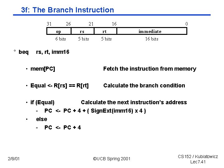
3 f: The Branch Instruction 31 26 op 6 bits ° beq 21 rs 5 bits 16 rt 5 bits 0 immediate 16 bits rs, rt, imm 16 • mem[PC] Fetch the instruction from memory • Equal < R[rs] == R[rt] Calculate the branch condition • if (Equal) Calculate the next instruction’s address - PC < PC + 4 + ( Sign. Ext(imm 16) x 4 ) • else - PC < PC + 4 2/8/01 ©UCB Spring 2001 CS 152 / Kubiatowicz Lec 7. 41

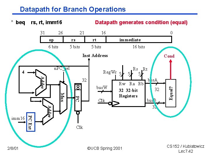
Datapath for Branch Operations rs, rt, imm 16 31 Datapath generates condition (equal) 26 op 6 bits 21 rs 5 bits 16 rt 5 bits 0 immediate 16 bits Inst Address n. PC_sel 4 Adder Reg. Wr 5 bus. W PC Mux 00 32 Clk 5 Rs 5 Rt Rw Ra Rb 32 32 -bit Registers Adder 2/8/01 PC Ext imm 16 Cond bus. A 32 bus. B 32 Equal? ° beq Clk ©UCB Spring 2001 CS 152 / Kubiatowicz Lec 7. 42

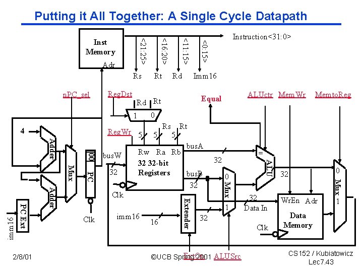
Putting it All Together: A Single Cycle Datapath n. PC_sel Reg. Dst 00 Rs Memto. Reg 5 Rt 16 Extender imm 16 = 32 0 1 32 Data In 32 Ext. Op ©UCB Spring 2001 ALUSrc Clk 0 32 Mux bus. A Rw Ra Rb 32 32 -bit Registers bus. B 32 Mux PC Mux Adder imm 16 5 Clk ALUctr Mem. Wr Equal ALU Adder PC Ext 2/8/01 32 Imm 16 0 Reg. Wr 5 bus. W Rd Rd Rt 1 4 Rt Instruction<31: 0> <0: 15> Rs <11: 15> Adr <16: 20> <21: 25> Inst Memory Wr. En Adr 1 Data Memory CS 152 / Kubiatowicz Lec 7. 43

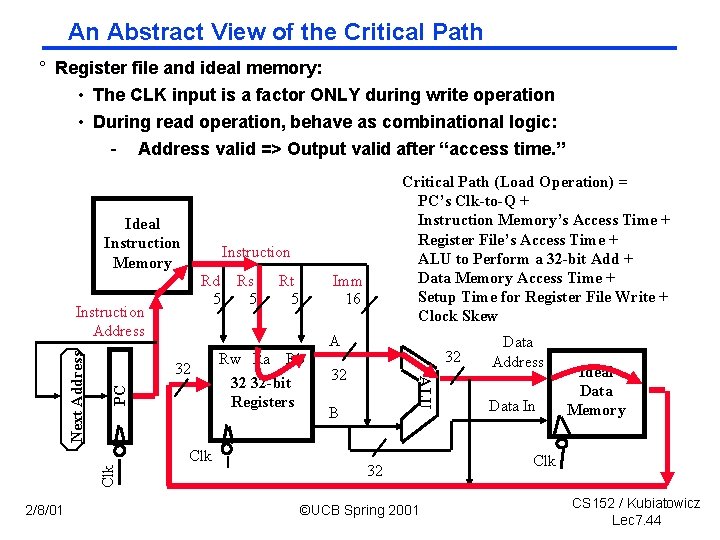
An Abstract View of the Critical Path ° Register file and ideal memory: • The CLK input is a factor ONLY during write operation • During read operation, behave as combinational logic: - Address valid => Output valid after “access time. ” Ideal Instruction Memory Instruction Rd Rs 5 5 Imm 16 A PC 32 Clk Rt 5 Rw Ra Rb 32 32 -bit Registers 32 32 ALU Next Address Instruction Address 2/8/01 Critical Path (Load Operation) = PC’s Clk-to-Q + Instruction Memory’s Access Time + Register File’s Access Time + ALU to Perform a 32 -bit Add + Data Memory Access Time + Setup Time for Register File Write + Clock Skew B 32 ©UCB Spring 2001 Data Address Data In Ideal Data Memory Clk CS 152 / Kubiatowicz Lec 7. 44

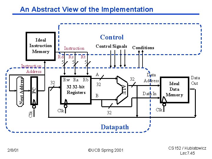
An Abstract View of the Implementation Control Ideal Instruction Memory Rd Rs 5 5 A Clk PC 32 Rw Ra Rb 32 32 -bit Registers Clk Conditions Rt 5 32 32 ALU Next Address Instruction Address Control Signals Instruction B 32 Data Address Data In Ideal Data Memory Data Out Clk Datapath 2/8/01 ©UCB Spring 2001 CS 152 / Kubiatowicz Lec 7. 45

Steps 4 & 5: Implement the control Next Time! 2/8/01 ©UCB Spring 2001 CS 152 / Kubiatowicz Lec 7. 46

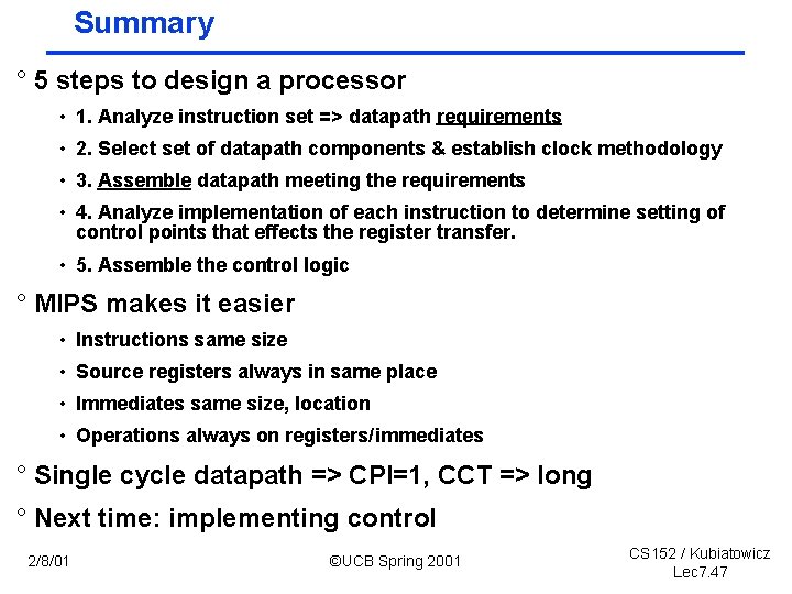
Summary ° 5 steps to design a processor • 1. Analyze instruction set => datapath requirements • 2. Select set of datapath components & establish clock methodology • 3. Assemble datapath meeting the requirements • 4. Analyze implementation of each instruction to determine setting of control points that effects the register transfer. • 5. Assemble the control logic ° MIPS makes it easier • Instructions same size • Source registers always in same place • Immediates same size, location • Operations always on registers/immediates ° Single cycle datapath => CPI=1, CCT => long ° Next time: implementing control 2/8/01 ©UCB Spring 2001 CS 152 / Kubiatowicz Lec 7. 47