CS 152 Computer Architecture and Engineering Lecture 21
- Slides: 42

CS 152 Computer Architecture and Engineering Lecture 21 Memory Systems (recap) Caches November 11 th, 2001 John Kubiatowicz (http. cs. berkeley. edu/~kubitron) lecture slides: http: //www inst. eecs. berkeley. edu/~cs 152/ 11/14/01 ©UCB Fall 2001 CS 152 / Kubiatowicz Lec 19. 1

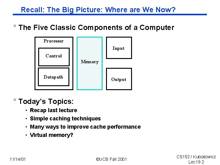
Recall: The Big Picture: Where are We Now? ° The Five Classic Components of a Computer Processor Input Control Memory Datapath Output ° Today’s Topics: • • 11/14/01 Recap last lecture Simple caching techniques Many ways to improve cache performance Virtual memory? ©UCB Fall 2001 CS 152 / Kubiatowicz Lec 19. 2

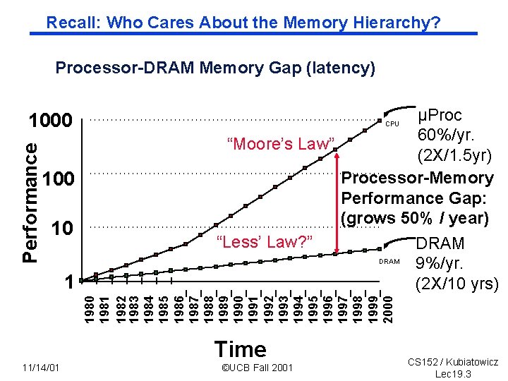
Recall: Who Cares About the Memory Hierarchy? Processor DRAM Memory Gap (latency) Performance 1000 10 1981 1982 1983 1984 1985 1986 1987 1988 1989 1990 1991 1992 1993 1994 1995 1996 1997 1998 1999 2000 1 µProc 60%/yr. “Moore’s Law” (2 X/1. 5 yr) Processor Memory Performance Gap: (grows 50% / year) “Less’ Law? ” DRAM 9%/yr. (2 X/10 yrs) CPU 11/14/01 Time ©UCB Fall 2001 CS 152 / Kubiatowicz Lec 19. 3

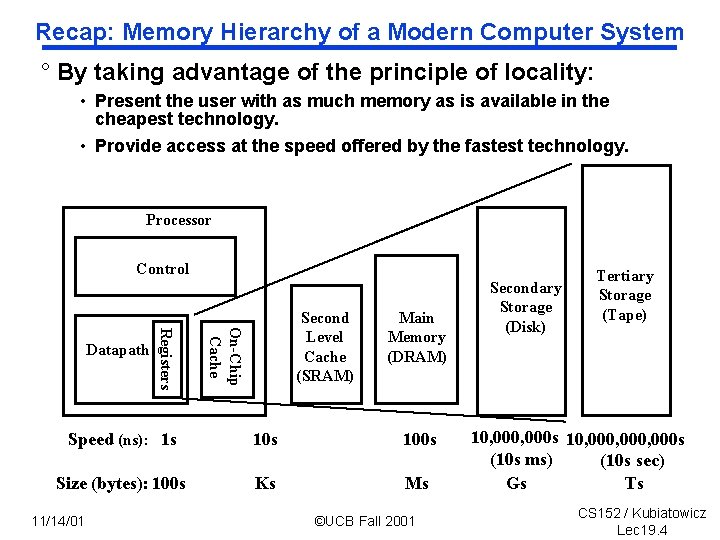
Recap: Memory Hierarchy of a Modern Computer System ° By taking advantage of the principle of locality: • Present the user with as much memory as is available in the cheapest technology. • Provide access at the speed offered by the fastest technology. Processor Control On-Chip Cache Registers Datapath Second Level Cache (SRAM) Main Memory (DRAM) Speed (ns): 1 s 100 s Size (bytes): 100 s Ks Ms 11/14/01 ©UCB Fall 2001 Secondary Storage (Disk) Tertiary Storage (Tape) 10, 000 s 10, 000, 000 s (10 s ms) (10 s sec) Gs Ts CS 152 / Kubiatowicz Lec 19. 4

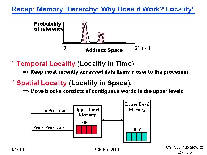
Recap: Memory Hierarchy: Why Does it Work? Locality! Probability of reference 0 2^n - 1 Address Space ° Temporal Locality (Locality in Time): => Keep most recently accessed data items closer to the processor ° Spatial Locality (Locality in Space): => Move blocks consists of contiguous words to the upper levels To Processor Upper Level Memory Lower Level Memory Blk X From Processor 11/14/01 Blk Y ©UCB Fall 2001 CS 152 / Kubiatowicz Lec 19. 5

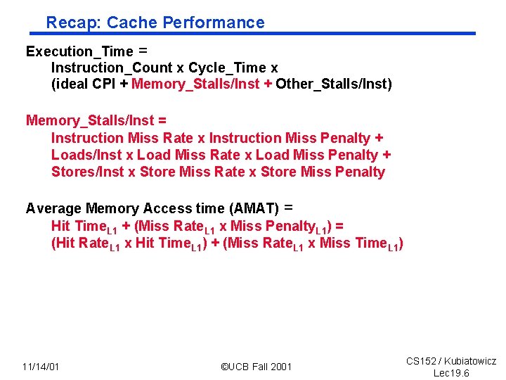
Recap: Cache Performance Execution_Time = Instruction_Count x Cycle_Time x (ideal CPI + Memory_Stalls/Inst + Other_Stalls/Inst) Memory_Stalls/Inst = Instruction Miss Rate x Instruction Miss Penalty + Loads/Inst x Load Miss Rate x Load Miss Penalty + Stores/Inst x Store Miss Rate x Store Miss Penalty Average Memory Access time (AMAT) = Hit Time. L 1 + (Miss Rate. L 1 x Miss Penalty. L 1) = (Hit Rate. L 1 x Hit Time. L 1) + (Miss Rate. L 1 x Miss Time. L 1) 11/14/01 ©UCB Fall 2001 CS 152 / Kubiatowicz Lec 19. 6

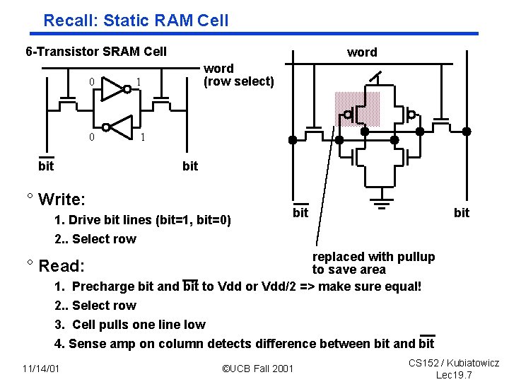
Recall: Static RAM Cell 6 Transistor SRAM Cell 0 0 bit word (row select) 1 1 bit ° Write: 1. Drive bit lines (bit=1, bit=0) 2. . Select row bit replaced with pullup to save area 1. Precharge bit and bit to Vdd or Vdd/2 => make sure equal! 2. . Select row 3. Cell pulls one line low 4. Sense amp on column detects difference between bit and bit ° Read: 11/14/01 ©UCB Fall 2001 CS 152 / Kubiatowicz Lec 19. 7

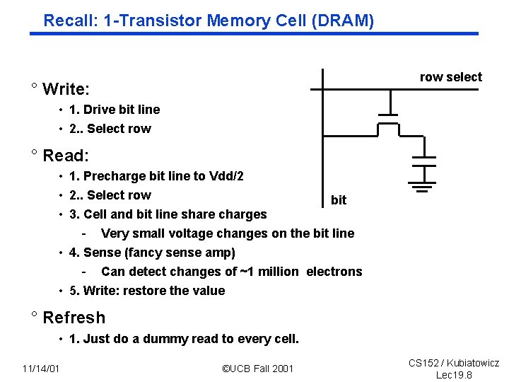
Recall: 1 Transistor Memory Cell (DRAM) row select ° Write: • 1. Drive bit line • 2. . Select row ° Read: • 1. Precharge bit line to Vdd/2 • 2. . Select row bit • 3. Cell and bit line share charges - Very small voltage changes on the bit line • 4. Sense (fancy sense amp) - Can detect changes of ~1 million electrons • 5. Write: restore the value ° Refresh • 1. Just do a dummy read to every cell. 11/14/01 ©UCB Fall 2001 CS 152 / Kubiatowicz Lec 19. 8

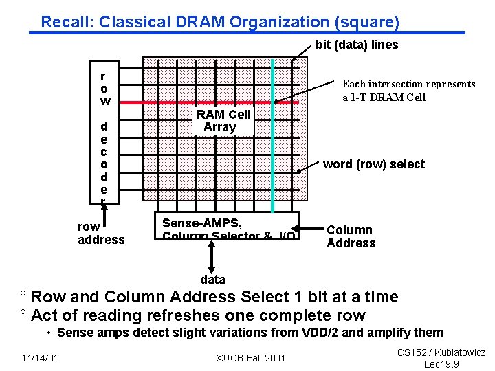
Recall: Classical DRAM Organization (square) bit (data) lines r o w d e c o d e r row address Each intersection represents a 1 -T DRAM Cell Array word (row) select Sense AMPS, Column Selector & I/O Column Address data ° Row and Column Address Select 1 bit at a time ° Act of reading refreshes one complete row • Sense amps detect slight variations from VDD/2 and amplify them 11/14/01 ©UCB Fall 2001 CS 152 / Kubiatowicz Lec 19. 9

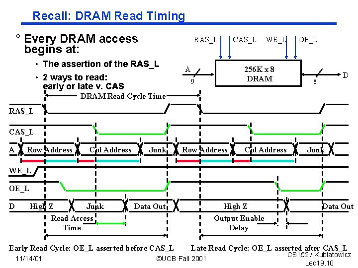
Recall: DRAM Read Timing ° Every DRAM access begins at: RAS_L • The assertion of the RAS_L • 2 ways to read: early or late v. CAS A CAS_L WE_L 256 K x 8 DRAM 9 OE_L D 8 DRAM Read Cycle Time RAS_L CAS_L A Row Address Col Address Junk WE_L OE_L D High Z Junk Read Access Time Data Out Early Read Cycle: OE_L asserted before CAS_L 11/14/01 High Z Output Enable Delay Data Out Late Read Cycle: OE_L asserted after CAS_L ©UCB Fall 2001 CS 152 / Kubiatowicz Lec 19. 10

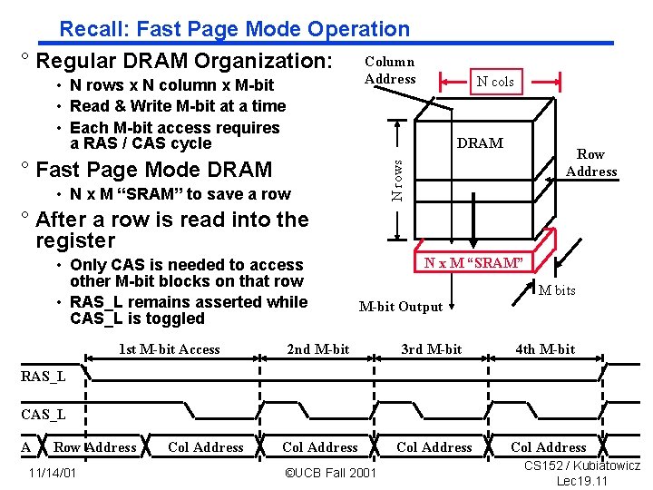
Recall: Fast Page Mode Operation ° Regular DRAM Organization: Column Address • N rows x N column x M bit • Read & Write M bit at a time • Each M bit access requires a RAS / CAS cycle N cols DRAM N rows ° Fast Page Mode DRAM Row Address • N x M “SRAM” to save a row ° After a row is read into the register • Only CAS is needed to access other M bit blocks on that row • RAS_L remains asserted while CAS_L is toggled 1 st M-bit Access N x M “SRAM” M bits M-bit Output 2 nd M-bit 3 rd M-bit 4 th M-bit Col Address RAS_L CAS_L A Row Address 11/14/01 Col Address ©UCB Fall 2001 CS 152 / Kubiatowicz Lec 19. 11

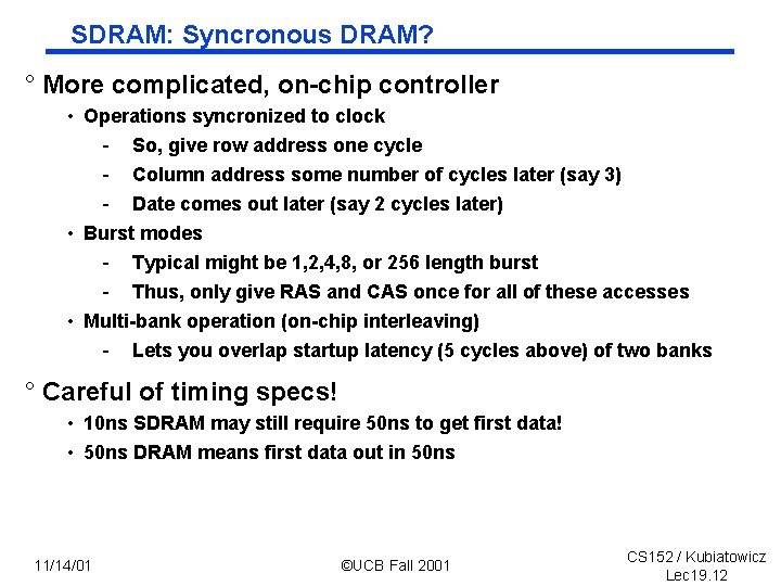
SDRAM: Syncronous DRAM? ° More complicated, on chip controller • Operations syncronized to clock - So, give row address one cycle - Column address some number of cycles later (say 3) - Date comes out later (say 2 cycles later) • Burst modes - Typical might be 1, 2, 4, 8, or 256 length burst - Thus, only give RAS and CAS once for all of these accesses • Multi bank operation (on chip interleaving) - Lets you overlap startup latency (5 cycles above) of two banks ° Careful of timing specs! • 10 ns SDRAM may still require 50 ns to get first data! • 50 ns DRAM means first data out in 50 ns 11/14/01 ©UCB Fall 2001 CS 152 / Kubiatowicz Lec 19. 12

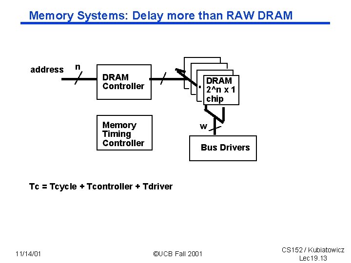
Memory Systems: Delay more than RAW DRAM address n DRAM Controller DRAM 2^n x 1 chip Memory Timing Controller w Bus Drivers Tc = Tcycle + Tcontroller + Tdriver 11/14/01 ©UCB Fall 2001 CS 152 / Kubiatowicz Lec 19. 13

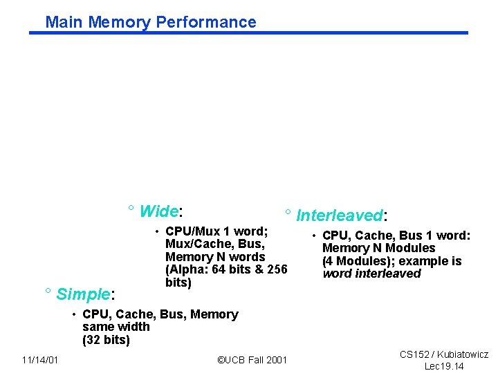
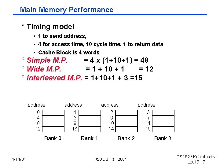
Main Memory Performance ° Wide: ° Simple: ° Interleaved: • CPU/Mux 1 word; Mux/Cache, Bus, Memory N words (Alpha: 64 bits & 256 bits) • CPU, Cache, Bus 1 word: Memory N Modules (4 Modules); example is word interleaved • CPU, Cache, Bus, Memory same width (32 bits) 11/14/01 ©UCB Fall 2001 CS 152 / Kubiatowicz Lec 19. 14

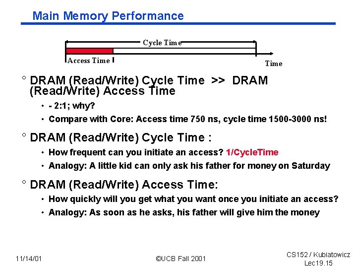
Main Memory Performance Cycle Time Access Time ° DRAM (Read/Write) Cycle Time >> DRAM (Read/Write) Access Time • 2: 1; why? • Compare with Core: Access time 750 ns, cycle time 1500 3000 ns! ° DRAM (Read/Write) Cycle Time : • How frequent can you initiate an access? 1/Cycle. Time • Analogy: A little kid can only ask his father for money on Saturday ° DRAM (Read/Write) Access Time: • How quickly will you get what you want once you initiate an access? • Analogy: As soon as he asks, his father will give him the money 11/14/01 ©UCB Fall 2001 CS 152 / Kubiatowicz Lec 19. 15

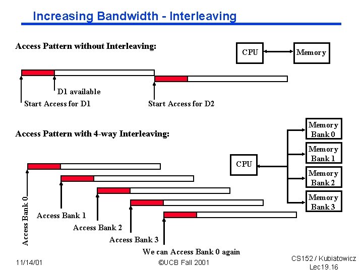
Increasing Bandwidth Interleaving Access Pattern without Interleaving: D 1 available Start Access for D 1 CPU Memory Start Access for D 2 Memory Bank 0 Access Pattern with 4 -way Interleaving: CPU Memory Bank 1 Access Bank 0 Memory Bank 2 Access Bank 1 Access Bank 2 Access Bank 3 We can Access Bank 0 again 11/14/01 ©UCB Fall 2001 Memory Bank 3 CS 152 / Kubiatowicz Lec 19. 16

Main Memory Performance ° Timing model • 1 to send address, • 4 for access time, 10 cycle time, 1 to return data • Cache Block is 4 words ° Simple M. P. = 4 x (1+10+1) = 48 ° Wide M. P. = 1 + 10 + 1 = 12 ° Interleaved M. P. = 1+10+1 + 3 =15 address 0 4 8 12 Bank 0 11/14/01 address 1 5 9 13 Bank 1 address 2 6 10 14 3 7 11 15 Bank 2 ©UCB Fall 2001 Bank 3 CS 152 / Kubiatowicz Lec 19. 17

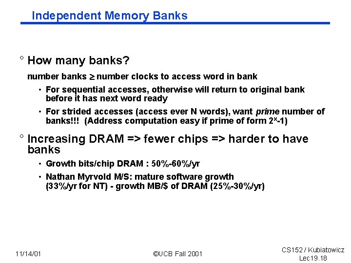
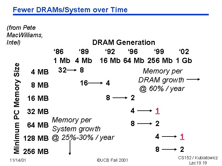
Independent Memory Banks ° How many banks? number banks number clocks to access word in bank • For sequential accesses, otherwise will return to original bank before it has next word ready • For strided accesses (access ever N words), want prime number of banks!!! (Address computation easy if prime of form 2 x 1) ° Increasing DRAM => fewer chips => harder to have banks • Growth bits/chip DRAM : 50% 60%/yr • Nathan Myrvold M/S: mature software growth (33%/yr for NT) growth MB/$ of DRAM (25% 30%/yr) 11/14/01 ©UCB Fall 2001 CS 152 / Kubiatowicz Lec 19. 18

Fewer DRAMs/System over Time Minimum PC Memory Size (from Pete Mac. Williams, Intel) DRAM Generation ‘ 86 ‘ 89 ‘ 92 ‘ 96 ‘ 99 ‘ 02 1 Mb 4 Mb 16 Mb 64 Mb 256 Mb 1 Gb 8 Memory per 4 MB 32 DRAM growth 16 4 8 MB @ 60% / year 8 2 16 MB 32 MB Memory per 64 MB System growth 128 MB @ 25%-30% / year 256 MB 11/14/01 ©UCB Fall 2001 4 1 8 2 CS 152 / Kubiatowicz Lec 19. 19

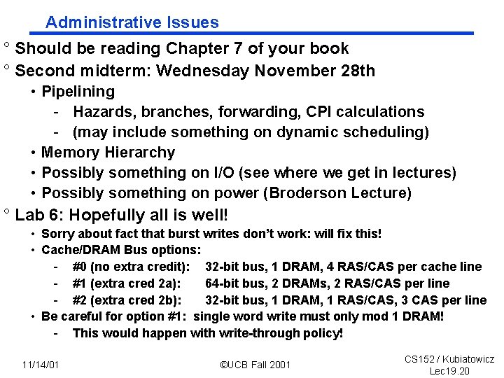
Administrative Issues ° Should be reading Chapter 7 of your book ° Second midterm: Wednesday November 28 th • Pipelining - Hazards, branches, forwarding, CPI calculations - (may include something on dynamic scheduling) • Memory Hierarchy • Possibly something on I/O (see where we get in lectures) • Possibly something on power (Broderson Lecture) ° Lab 6: Hopefully all is well! • Sorry about fact that burst writes don’t work: will fix this! • Cache/DRAM Bus options: - #0 (no extra credit): 32 bit bus, 1 DRAM, 4 RAS/CAS per cache line - #1 (extra cred 2 a): 64 bit bus, 2 DRAMs, 2 RAS/CAS per line - #2 (extra cred 2 b): 32 bit bus, 1 DRAM, 1 RAS/CAS, 3 CAS per line • Be careful for option #1: single word write must only mod 1 DRAM! - This would happen with write through policy! 11/14/01 ©UCB Fall 2001 CS 152 / Kubiatowicz Lec 19. 20

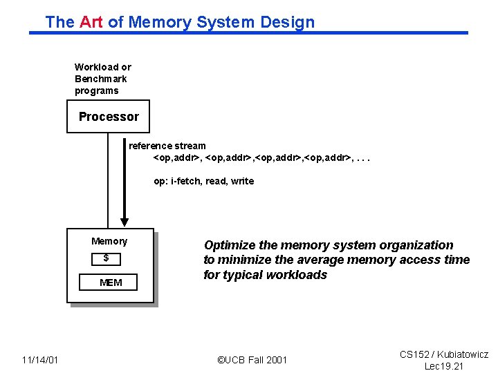
The Art of Memory System Design Workload or Benchmark programs Processor reference stream <op, addr>, . . . op: i fetch, read, write Memory $ MEM 11/14/01 Optimize the memory system organization to minimize the average memory access time for typical workloads ©UCB Fall 2001 CS 152 / Kubiatowicz Lec 19. 21

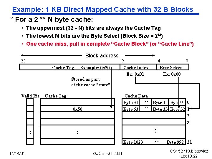
Example: 1 KB Direct Mapped Cache with 32 B Blocks ° For a 2 ** N byte cache: • The uppermost (32 N) bits are always the Cache Tag • The lowest M bits are the Byte Select (Block Size = 2 M) • One cache miss, pull in complete “Cache Block” (or “Cache Line”) Block address Cache Tag Example: 0 x 50 Stored as part of the cache “state” Cache Data Byte 31 Byte 63 Cache Tag : : Valid Bit 9 Cache Index Ex: 0 x 01 0 x 50 : Byte 1 Byte 0 0 Byte 33 Byte 32 1 2 3 : : Byte 1023 11/14/01 4 0 Byte Select Ex: 0 x 00 ©UCB Fall 2001 : 31 Byte 992 31 CS 152 / Kubiatowicz Lec 19. 22

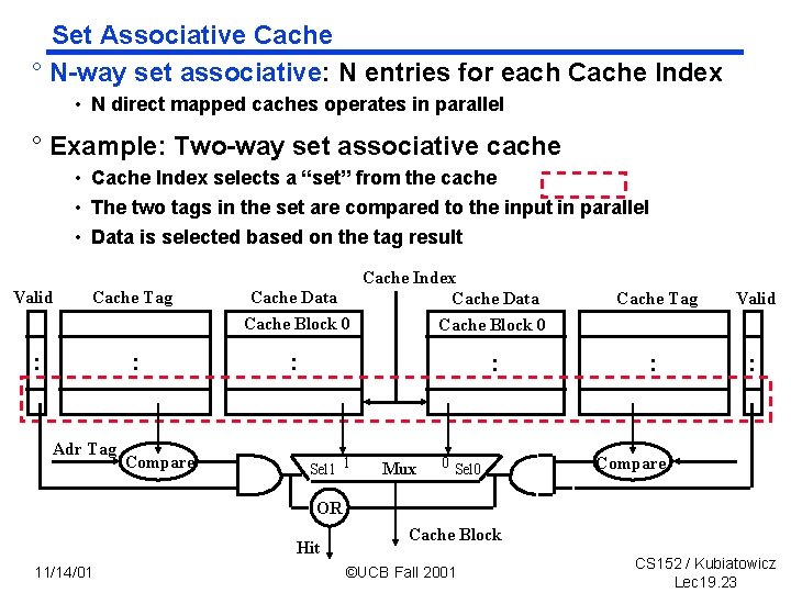
Set Associative Cache ° N way set associative: N entries for each Cache Index • N direct mapped caches operates in parallel ° Example: Two way set associative cache • Cache Index selects a “set” from the cache • The two tags in the set are compared to the input in parallel • Data is selected based on the tag result Valid Cache Tag : : Adr Tag Compare Cache Index Cache Data Cache Block 0 : : Sel 1 1 Mux 0 Sel 0 Cache Tag Valid : : Compare OR Hit 11/14/01 Cache Block ©UCB Fall 2001 CS 152 / Kubiatowicz Lec 19. 23

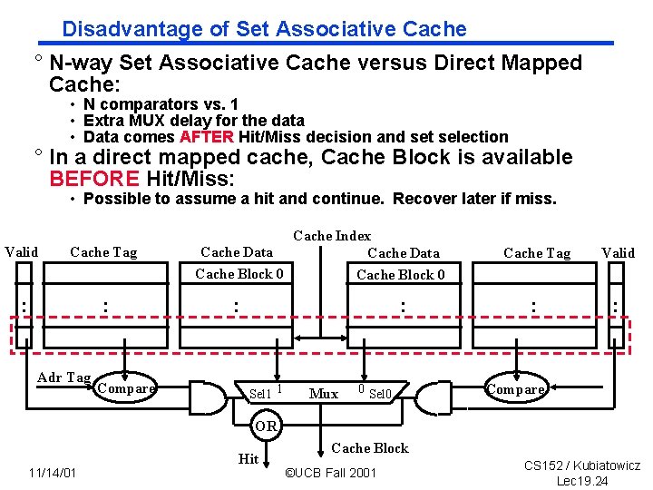
Disadvantage of Set Associative Cache ° N way Set Associative Cache versus Direct Mapped Cache: • N comparators vs. 1 • Extra MUX delay for the data • Data comes AFTER Hit/Miss decision and set selection ° In a direct mapped cache, Cache Block is available BEFORE Hit/Miss: • Possible to assume a hit and continue. Recover later if miss. Valid Cache Tag : : Adr Tag Compare Cache Index Cache Data Cache Block 0 : : Sel 1 1 Mux 0 Sel 0 Cache Tag Valid : : Compare OR 11/14/01 Hit Cache Block ©UCB Fall 2001 CS 152 / Kubiatowicz Lec 19. 24

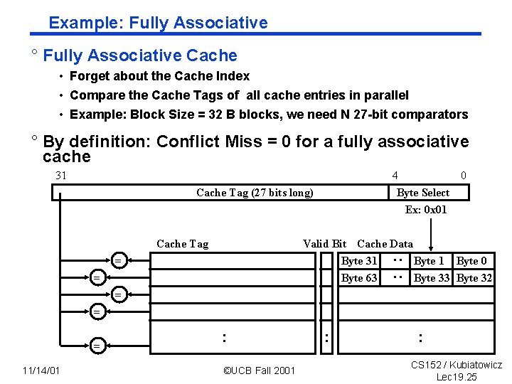
Example: Fully Associative ° Fully Associative Cache • Forget about the Cache Index • Compare the Cache Tags of all cache entries in parallel • Example: Block Size = 32 B blocks, we need N 27 bit comparators ° By definition: Conflict Miss = 0 for a fully associative cache 31 4 0 Byte Select Ex: 0 x 01 Cache Tag (27 bits long) Cache Tag Valid Bit Cache Data Byte 31 Byte 0 Byte 63 Byte 32 : : = = = 11/14/01 : ©UCB Fall 2001 : : CS 152 / Kubiatowicz Lec 19. 25

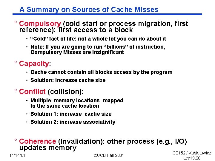
A Summary on Sources of Cache Misses ° Compulsory (cold start or process migration, first reference): first access to a block • “Cold” fact of life: not a whole lot you can do about it • Note: If you are going to run “billions” of instruction, Compulsory Misses are insignificant ° Capacity: • Cache cannot contain all blocks access by the program • Solution: increase cache size ° Conflict (collision): • Multiple memory locations mapped to the same cache location • Solution 1: increase cache size • Solution 2: increase associativity ° Coherence (Invalidation): other process (e. g. , I/O) updates memory 11/14/01 ©UCB Fall 2001 CS 152 / Kubiatowicz Lec 19. 26

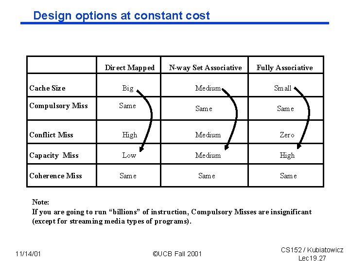
Design options at constant cost Direct Mapped Cache Size Compulsory Miss Big Same N-way Set Associative Medium Same Fully Associative Small Same Conflict Miss High Medium Zero Capacity Miss Low Medium High Coherence Miss Same Note: If you are going to run “billions” of instruction, Compulsory Misses are insignificant (except for streaming media types of programs). 11/14/01 ©UCB Fall 2001 CS 152 / Kubiatowicz Lec 19. 27

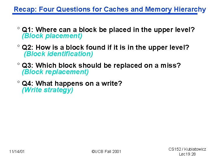
Recap: Four Questions for Caches and Memory Hierarchy ° Q 1: Where can a block be placed in the upper level? (Block placement) ° Q 2: How is a block found if it is in the upper level? (Block identification) ° Q 3: Which block should be replaced on a miss? (Block replacement) ° Q 4: What happens on a write? (Write strategy) 11/14/01 ©UCB Fall 2001 CS 152 / Kubiatowicz Lec 19. 28

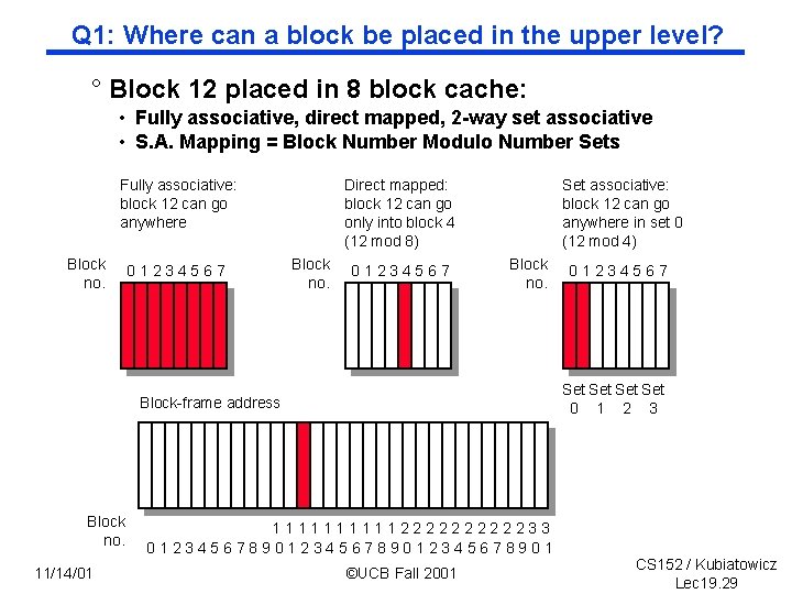
Q 1: Where can a block be placed in the upper level? ° Block 12 placed in 8 block cache: • Fully associative, direct mapped, 2 way set associative • S. A. Mapping = Block Number Modulo Number Sets Direct mapped: block 12 can go only into block 4 (12 mod 8) Fully associative: block 12 can go anywhere Block no. 01234567 Set associative: block 12 can go anywhere in set 0 (12 mod 4) Block no. Set Set 0 1 2 3 Block-frame address Block no. 11/14/01 01234567 111112222233 0123456789012345678901 ©UCB Fall 2001 CS 152 / Kubiatowicz Lec 19. 29

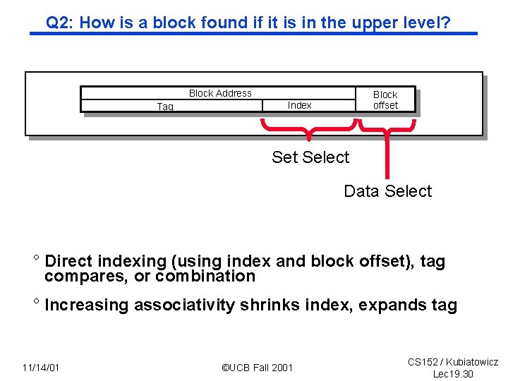
Q 2: How is a block found if it is in the upper level? Block Address Tag Block offset Index Set Select Data Select ° Direct indexing (using index and block offset), tag compares, or combination ° Increasing associativity shrinks index, expands tag 11/14/01 ©UCB Fall 2001 CS 152 / Kubiatowicz Lec 19. 30

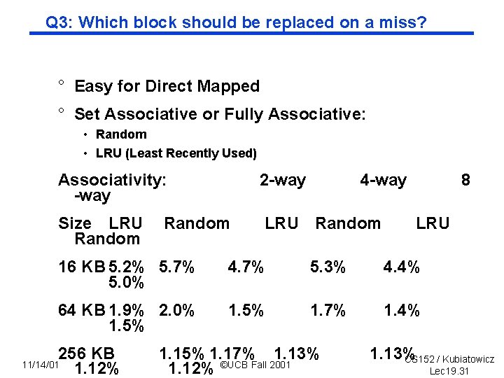
Q 3: Which block should be replaced on a miss? ° Easy for Direct Mapped ° Set Associative or Fully Associative: • Random • LRU (Least Recently Used) Associativity: way 2 way Size LRU Random 4 way 8 LRU 16 KB 5. 2% 5. 7% 5. 0% 4. 7% 5. 3% 4. 4% 64 KB 1. 9% 2. 0% 1. 5% 1. 7% 1. 4% 256 KB 1. 12% 11/14/01 1. 15% 1. 17% 1. 13% 1. 12% ©UCB Fall 2001 1. 13% CS 152 / Kubiatowicz Lec 19. 31

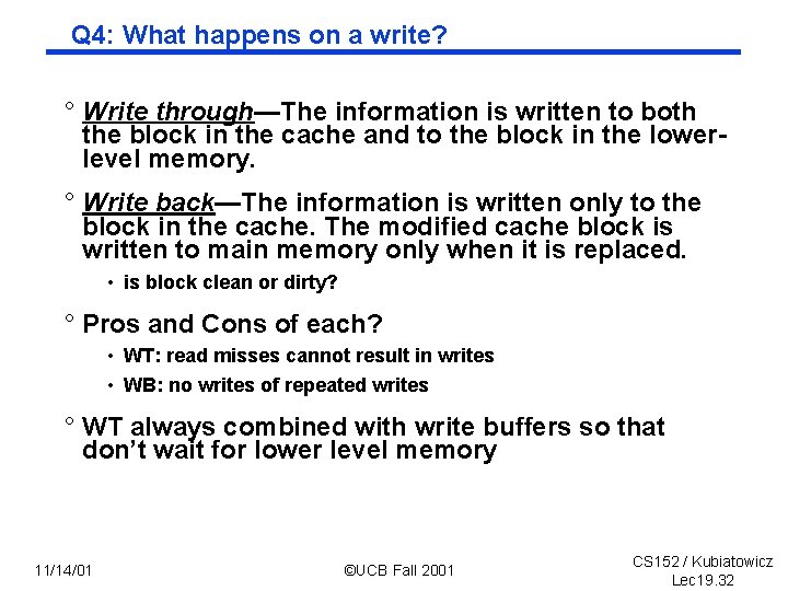
Q 4: What happens on a write? ° Write through—The information is written to both the block in the cache and to the block in the lower level memory. ° Write back—The information is written only to the block in the cache. The modified cache block is written to main memory only when it is replaced. • is block clean or dirty? ° Pros and Cons of each? • WT: read misses cannot result in writes • WB: no writes of repeated writes ° WT always combined with write buffers so that don’t wait for lower level memory 11/14/01 ©UCB Fall 2001 CS 152 / Kubiatowicz Lec 19. 32

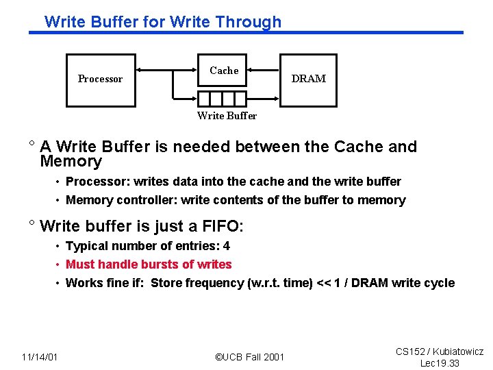
Write Buffer for Write Through Processor Cache DRAM Write Buffer ° A Write Buffer is needed between the Cache and Memory • Processor: writes data into the cache and the write buffer • Memory controller: write contents of the buffer to memory ° Write buffer is just a FIFO: • Typical number of entries: 4 • Must handle bursts of writes • Works fine if: Store frequency (w. r. t. time) << 1 / DRAM write cycle 11/14/01 ©UCB Fall 2001 CS 152 / Kubiatowicz Lec 19. 33

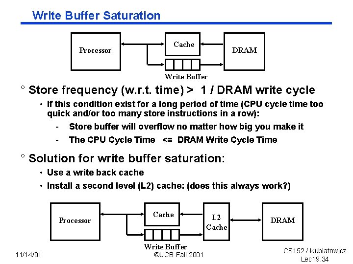
Write Buffer Saturation Processor Cache DRAM Write Buffer ° Store frequency (w. r. t. time) > 1 / DRAM write cycle • If this condition exist for a long period of time (CPU cycle time too quick and/or too many store instructions in a row): - Store buffer will overflow no matter how big you make it - The CPU Cycle Time <= DRAM Write Cycle Time ° Solution for write buffer saturation: • Use a write back cache • Install a second level (L 2) cache: (does this always work? ) Processor 11/14/01 Cache Write Buffer ©UCB Fall 2001 L 2 Cache DRAM CS 152 / Kubiatowicz Lec 19. 34

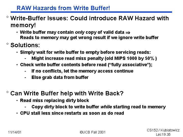
RAW Hazards from Write Buffer! ° Write Buffer Issues: Could introduce RAW Hazard with memory! • Write buffer may contain only copy of valid data Reads to memory may get wrong result if we ignore write buffer ° Solutions: • Simply wait for write buffer to empty before servicing reads: - Might increase read miss penalty (old MIPS 1000 by 50% ) • Check write buffer contents before read (“fully associative”); - If no conflicts, let the memory access continue - Else grab data from buffer ° Can Write Buffer help with Write Back? • Read miss replacing dirty block - Copy dirty block to write buffer while starting read to memory • CPU stall less since restarts as soon as do read 11/14/01 ©UCB Fall 2001 CS 152 / Kubiatowicz Lec 19. 35

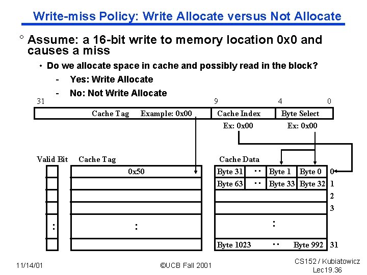
Write miss Policy: Write Allocate versus Not Allocate ° Assume: a 16 bit write to memory location 0 x 0 and causes a miss • Do we allocate space in cache and possibly read in the block? - Yes: Write Allocate - No: Not Write Allocate 31 Valid Bit Example: 0 x 00 Cache Tag Cache Data Byte 31 Byte 63 : : : 0 x 50 Byte 1 Byte 0 0 Byte 33 Byte 32 1 2 3 : : Byte 1023 11/14/01 4 0 Byte Select Ex: 0 x 00 ©UCB Fall 2001 : Cache Tag 9 Cache Index Ex: 0 x 00 Byte 992 31 CS 152 / Kubiatowicz Lec 19. 36

Impact of Memory Hierarchy on Algorithms ° Today CPU time is a function of (ops, cache misses) ° What does this mean to Compilers, Data structures, Algorithms? • Quicksort: fastest comparison based sorting algorithm when keys fit in memory • Radix sort: also called “linear time” sort For keys of fixed length and fixed radix a constant number of passes over the data is sufficient independent of the number of keys ° “The Influence of Caches on the Performance of Sorting” by A. La. Marca and R. E. Ladner. Proceedings of the Eighth Annual ACM-SIAM Symposium on Discrete Algorithms, January, 1997, 370 379. • For Alphastation 250, 32 byte blocks, direct mapped L 2 2 MB cache, 8 byte keys, from 4000 to 4000000 11/14/01 ©UCB Fall 2001 CS 152 / Kubiatowicz Lec 19. 37

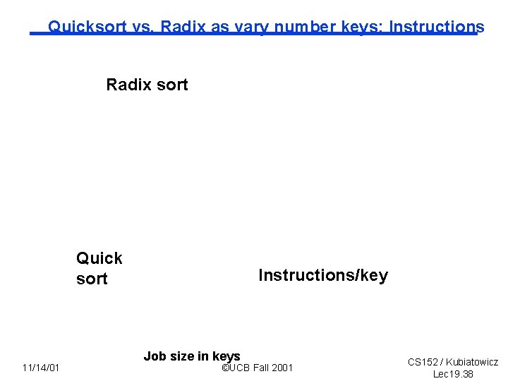
Quicksort vs. Radix as vary number keys: Instructions Radix sort Quick sort 11/14/01 Instructions/key Job size in keys ©UCB Fall 2001 CS 152 / Kubiatowicz Lec 19. 38

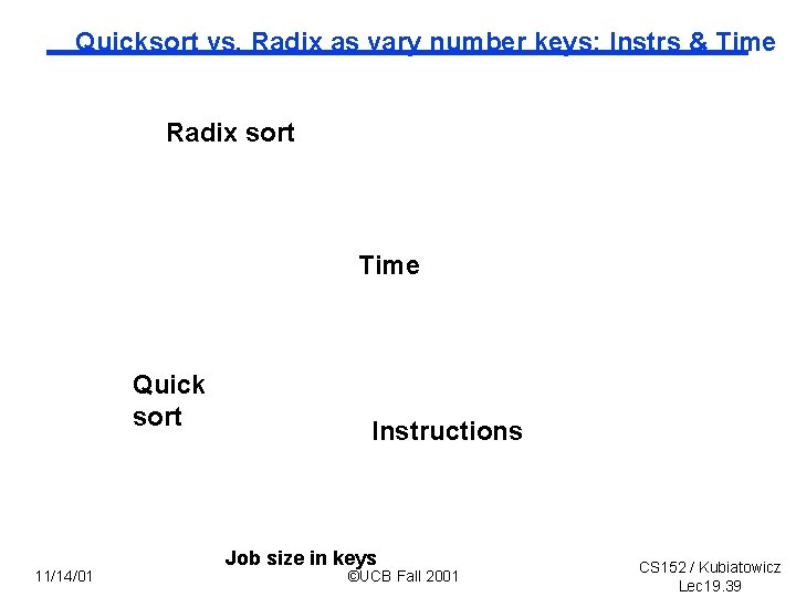
Quicksort vs. Radix as vary number keys: Instrs & Time Radix sort Time Quick sort 11/14/01 Instructions Job size in keys ©UCB Fall 2001 CS 152 / Kubiatowicz Lec 19. 39

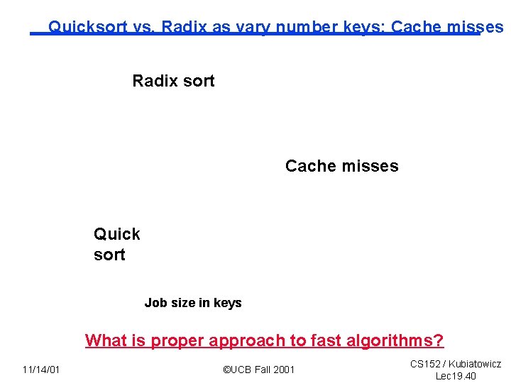
Quicksort vs. Radix as vary number keys: Cache misses Radix sort Cache misses Quick sort Job size in keys What is proper approach to fast algorithms? 11/14/01 ©UCB Fall 2001 CS 152 / Kubiatowicz Lec 19. 40

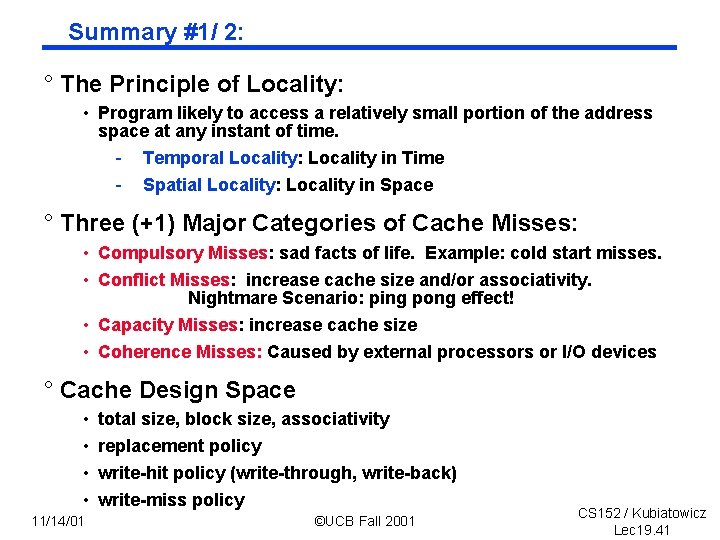
Summary #1/ 2: ° The Principle of Locality: • Program likely to access a relatively small portion of the address space at any instant of time. - Temporal Locality: Locality in Time - Spatial Locality: Locality in Space ° Three (+1) Major Categories of Cache Misses: • Compulsory Misses: sad facts of life. Example: cold start misses. • Conflict Misses: increase cache size and/or associativity. Nightmare Scenario: ping pong effect! • Capacity Misses: increase cache size • Coherence Misses: Caused by external processors or I/O devices ° Cache Design Space • • 11/14/01 total size, block size, associativity replacement policy write hit policy (write through, write back) write miss policy ©UCB Fall 2001 CS 152 / Kubiatowicz Lec 19. 41

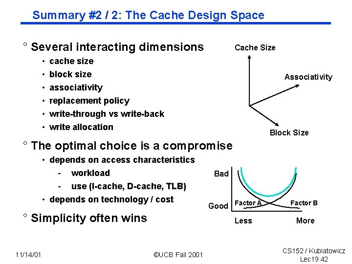
Summary #2 / 2: The Cache Design Space ° Several interacting dimensions • • • Cache Size cache size block size associativity replacement policy Associativity write through vs write back write allocation Block Size ° The optimal choice is a compromise • depends on access characteristics - workload - use (I cache, D cache, TLB) • depends on technology / cost ° Simplicity often wins 11/14/01 Bad Good Factor A Less ©UCB Fall 2001 Factor B More CS 152 / Kubiatowicz Lec 19. 42