CS 152 Computer Architecture and Engineering Lecture 12
- Slides: 40

CS 152 Computer Architecture and Engineering Lecture 12 – Memory and Interfaces 2005 -10 -11 John Lazzaro (www. cs. berkeley. edu/~lazzaro) TAs: David Marquardt and Udam Saini www-inst. eecs. berkeley. edu/~cs 152/ CS 152 L 12: Memory and Interfaces UC Regents Fall 2005 © UCB

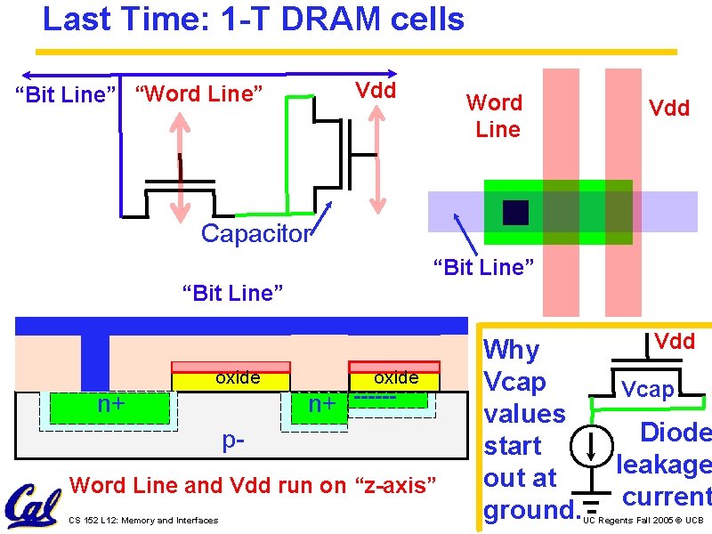
Last Time: 1 -T DRAM cells Vdd “Bit Line” “Word Line” Word Line Vdd Capacitor “Bit Line” oxide n+ ------ p. Word Line and Vdd run on “z-axis” CS 152 L 12: Memory and Interfaces Why Vcap values start out at ground. Vdd Vcap Diode leakage current UC Regents Fall 2005 © UCB

Today: Memory Technology Wrap-Up Static Memory Circuits: For SRAM memory cells and for flip-flops. Memory Arrays: Row decoders, column sense amps, array sizing. DRAM Interfaces: How the SDRAM chips on the Calinx board work. CS 152 L 12: Memory and Interfaces UC Regents Fall 2005 © UCB

Inverters CS 152 L 12: Memory and Interfaces UC Regents Fall 2005 © UCB

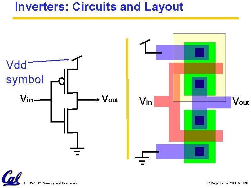
Inverters: Circuits and Layout Vdd symbol Vin CS 152 L 12: Memory and Interfaces Vout Vin Vout UC Regents Fall 2005 © UCB

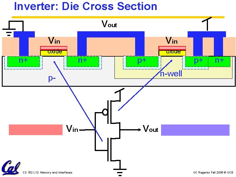
Inverter: Die Cross Section Vout Vin oxide n+ n+ p+ p+ n+ n-well p- Vin CS 152 L 12: Memory and Interfaces Vout UC Regents Fall 2005 © UCB

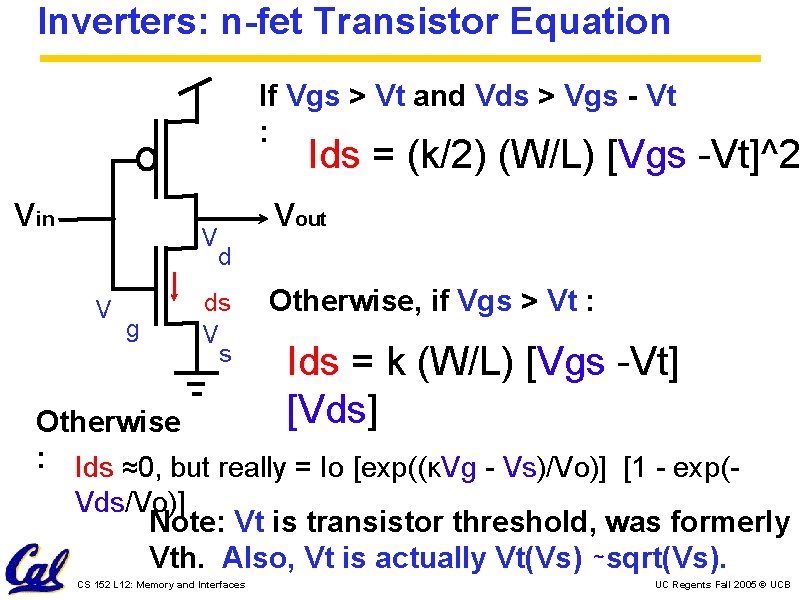
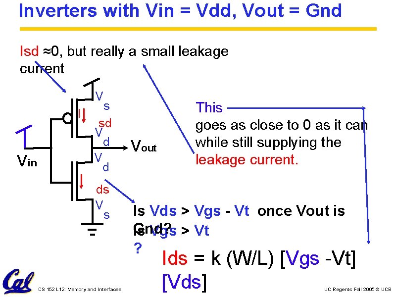
Inverters: n-fet Transistor Equation If Vgs > Vt and Vds > Vgs - Vt : Ids = (k/2) (W/L) [Vgs -Vt]^2 Vin V V I g Vout d ds V s Otherwise, if Vgs > Vt : Ids = k (W/L) [Vgs -Vt] [Vds] Otherwise : Ids ≈0, but really = Io [exp((κVg - Vs)/Vo)] [1 - exp(Vds/Vo)] Note: Vt is transistor threshold, was formerly Vth. Also, Vt is actually Vt(Vs) ∼sqrt(Vs). CS 152 L 12: Memory and Interfaces UC Regents Fall 2005 © UCB

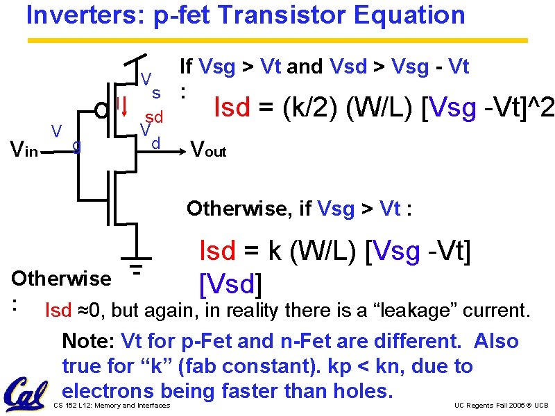
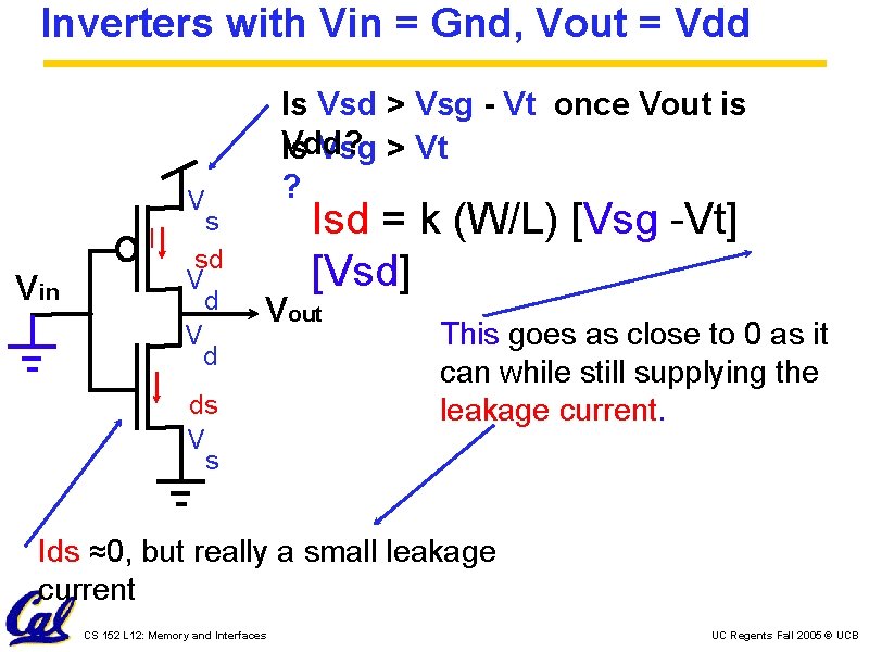
Inverters: p-fet Transistor Equation I Vin V g If Vsg > Vt and Vsd > Vsg - Vt V s : sd V d Isd = (k/2) (W/L) [Vsg -Vt]^2 Vout Otherwise, if Vsg > Vt : Isd = k (W/L) [Vsg -Vt] [Vsd] Otherwise : Isd ≈0, but again, in reality there is a “leakage” current. Note: Vt for p-Fet and n-Fet are different. Also true for “k” (fab constant). kp < kn, due to electrons being faster than holes. CS 152 L 12: Memory and Interfaces UC Regents Fall 2005 © UCB

Inverters with Vin = Gnd, Vout = Vdd Is Vsd > Vsg - Vt once Vout is Vdd? Is Vsg > Vt ? V I Vin I s sd V d Isd = k (W/L) [Vsg -Vt] [Vsd] Vout ds V s This goes as close to 0 as it can while still supplying the leakage current. Ids ≈0, but really a small leakage current CS 152 L 12: Memory and Interfaces UC Regents Fall 2005 © UCB

Inverters with Vin = Vdd, Vout = Gnd Isd ≈0, but really a small leakage current V I Vin I s sd V d ds V s CS 152 L 12: Memory and Interfaces Vout This goes as close to 0 as it can while still supplying the leakage current. Is Vds > Vgs - Vt once Vout is Gnd? Is Vgs > Vt ? Ids = k (W/L) [Vgs -Vt] [Vds] UC Regents Fall 2005 © UCB

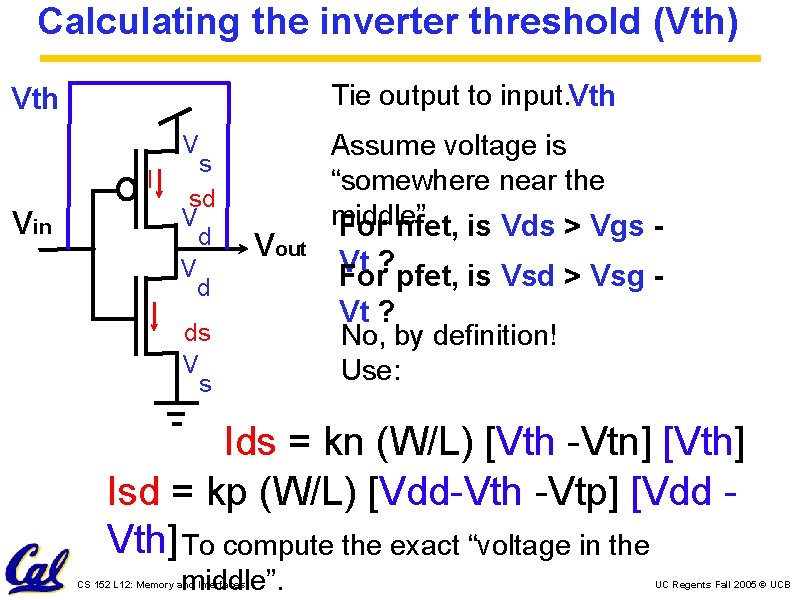
Calculating the inverter threshold (Vth) Tie output to input. Vth V I Vin I s sd V d Vout ds V s Assume voltage is “somewhere near the middle” For nfet, is Vds > Vgs - Vt For? pfet, is Vsd > Vsg Vt ? No, by definition! Use: Ids = kn (W/L) [Vth -Vtn] [Vth] Isd = kp (W/L) [Vdd-Vth -Vtp] [Vdd Vth] To compute the exact “voltage in the middle”. CS 152 L 12: Memory and Interfaces UC Regents Fall 2005 © UCB

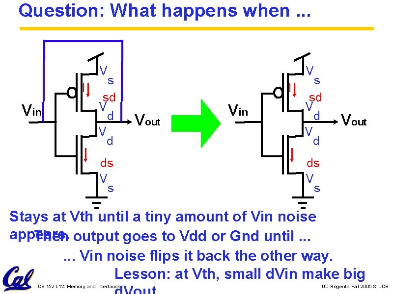
Question: What happens when. . . V V I Vin I s sd V d ds V s I Vout Vin I s sd V d Vout ds V s Stays at Vth until a tiny amount of Vin noise appears. Then output goes to Vdd or Gnd until. . . Vin noise flips it back the other way. Lesson: at Vth, small d. Vin make big CS 152 L 12: Memory and Interfaces UC Regents Fall 2005 © UCB

Static Memory Circuits Dynamic Memory: Circuit remembers for a fraction of a second. Static Memory: Circuit remembers as long as the power is on. Non-volatile Memory: Circuit remembers for many years, even if power is off. CS 152 L 12: Memory and Interfaces UC Regents Fall 2005 © UCB

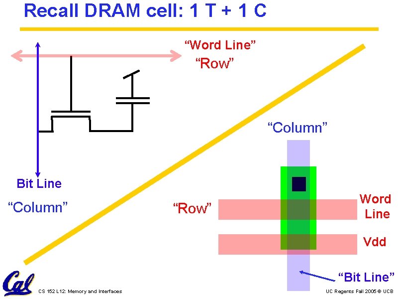
Recall DRAM cell: 1 T + 1 C “Word Line” “Row” “Column” Bit Line “Column” “Row” Word Line Vdd “Bit Line” CS 152 L 12: Memory and Interfaces UC Regents Fall 2005 © UCB

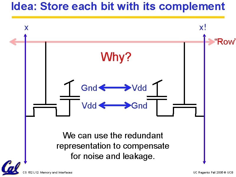
Idea: Store each bit with its complement x x! “Row” Why? Gnd Vdd Gnd We can use the redundant representation to compensate for noise and leakage. CS 152 L 12: Memory and Interfaces UC Regents Fall 2005 © UCB

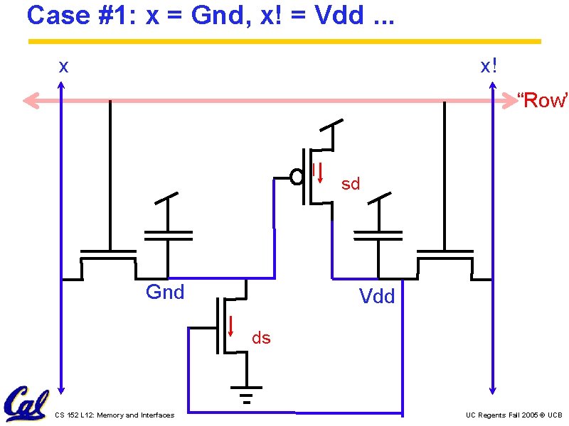
Case #1: x = Gnd, x! = Vdd. . . x x! “Row” I Gnd Vdd I CS 152 L 12: Memory and Interfaces sd ds UC Regents Fall 2005 © UCB

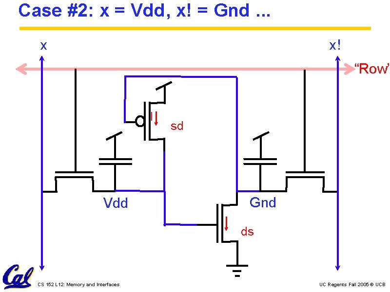
Case #2: x = Vdd, x! = Gnd. . . x x! “Row” I sd Gnd Vdd I CS 152 L 12: Memory and Interfaces ds UC Regents Fall 2005 © UCB

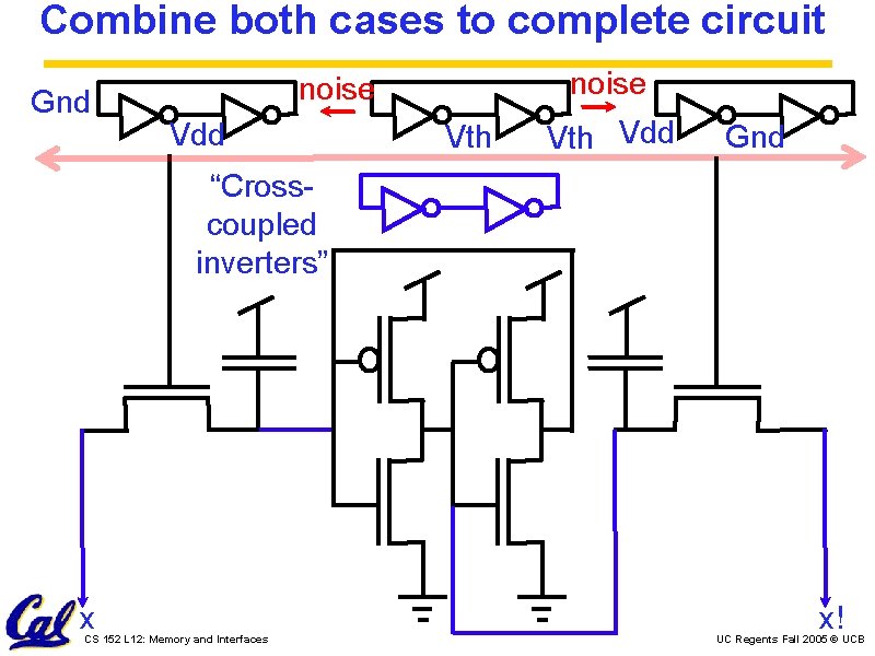
Combine both cases to complete circuit Gnd noise Vdd Vth Vdd Gnd “Crosscoupled inverters” x CS 152 L 12: Memory and Interfaces x! UC Regents Fall 2005 © UCB

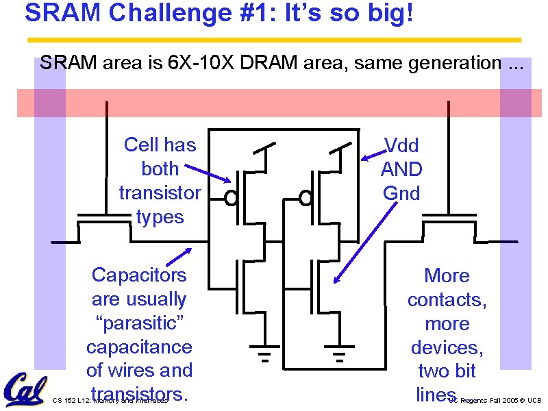
SRAM Challenge #1: It’s so big! SRAM area is 6 X-10 X DRAM area, same generation. . . Cell has both transistor types Capacitors are usually “parasitic” capacitance of wires and transistors. CS 152 L 12: Memory and Interfaces Vdd AND Gnd More contacts, more devices, two bit lines. . . UC Regents Fall 2005 © UCB

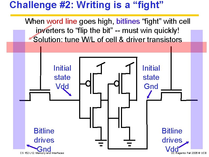
Challenge #2: Writing is a “fight” When word line goes high, bitlines “fight” with cell inverters to “flip the bit” -- must win quickly! Solution: tune W/L of cell & driver transistors Initial state Vdd Bitline drives Gnd CS 152 L 12: Memory and Interfaces Initial state Gnd Bitline drives Vdd UC Regents Fall 2005 © UCB

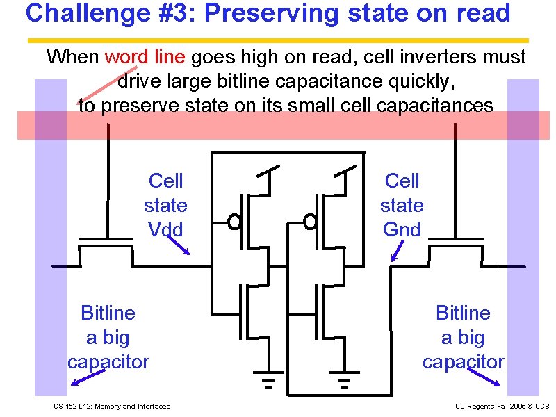
Challenge #3: Preserving state on read When word line goes high on read, cell inverters must drive large bitline capacitance quickly, to preserve state on its small cell capacitances Cell state Vdd Bitline a big capacitor CS 152 L 12: Memory and Interfaces Cell state Gnd Bitline a big capacitor UC Regents Fall 2005 © UCB

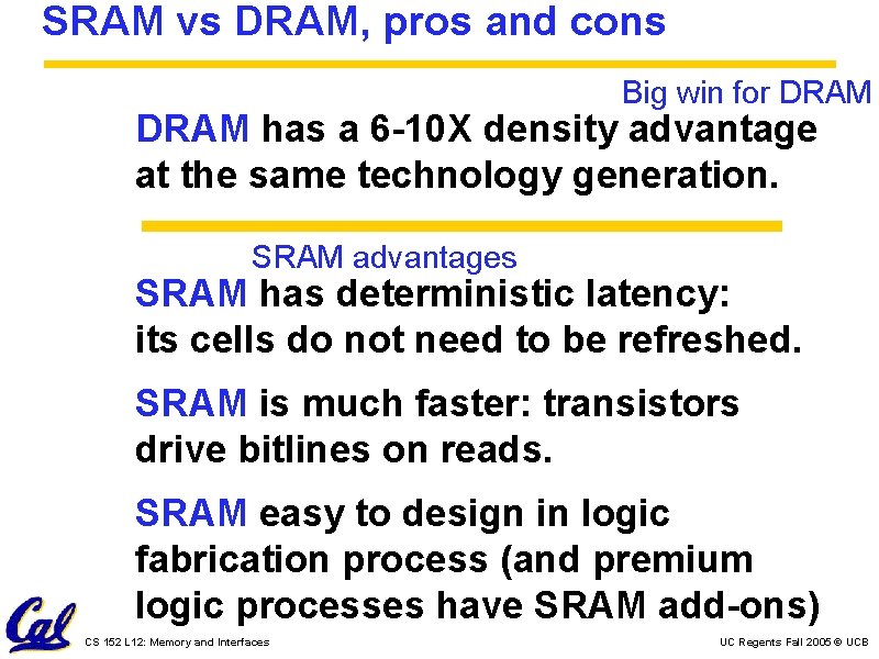
SRAM vs DRAM, pros and cons Big win for DRAM has a 6 -10 X density advantage at the same technology generation. SRAM advantages SRAM has deterministic latency: its cells do not need to be refreshed. SRAM is much faster: transistors drive bitlines on reads. SRAM easy to design in logic fabrication process (and premium logic processes have SRAM add-ons) CS 152 L 12: Memory and Interfaces UC Regents Fall 2005 © UCB

Flip Flops Revisited CS 152 L 12: Memory and Interfaces UC Regents Fall 2005 © UCB

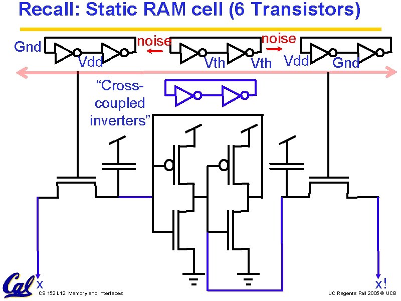
Recall: Static RAM cell (6 Transistors) Gnd noise Vdd Vth Vdd Gnd “Crosscoupled inverters” x CS 152 L 12: Memory and Interfaces x! UC Regents Fall 2005 © UCB

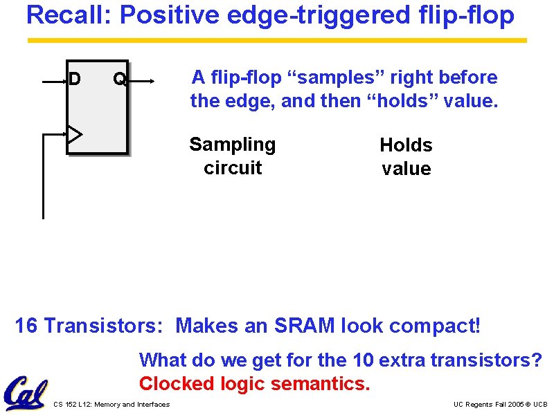
Recall: Positive edge-triggered flip-flop D A flip-flop “samples” right before the edge, and then “holds” value. Q Sampling circuit Holds value 16 Transistors: Makes an SRAM look compact! What do we get for the 10 extra transistors? Clocked logic semantics. CS 152 L 12: Memory and Interfaces UC Regents Fall 2005 © UCB

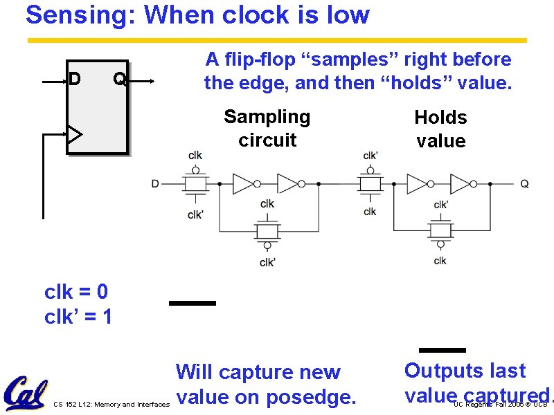
Sensing: When clock is low D Q A flip-flop “samples” right before the edge, and then “holds” value. Sampling circuit Holds value clk = 0 clk’ = 1 CS 152 L 12: Memory and Interfaces Will capture new value on posedge. Outputs last value captured. UC Regents Fall 2005 © UCB

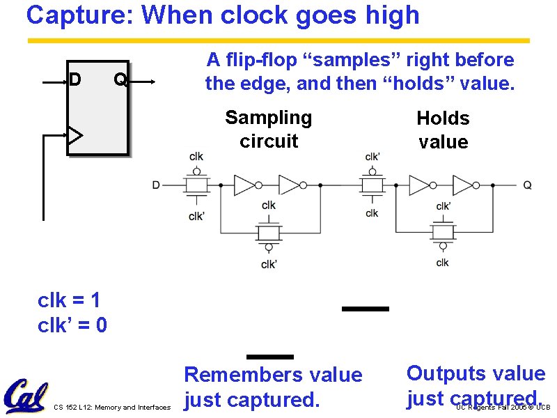
Capture: When clock goes high D Q A flip-flop “samples” right before the edge, and then “holds” value. Sampling circuit Holds value clk = 1 clk’ = 0 CS 152 L 12: Memory and Interfaces Remembers value just captured. Outputs value just captured. UC Regents Fall 2005 © UCB

Admin: Final Xilinx Checkoff Friday. . . Lab report due Monday, 11: 59 PM. CS 152 L 12: Memory and Interfaces UC Regents Fall 2005 © UCB

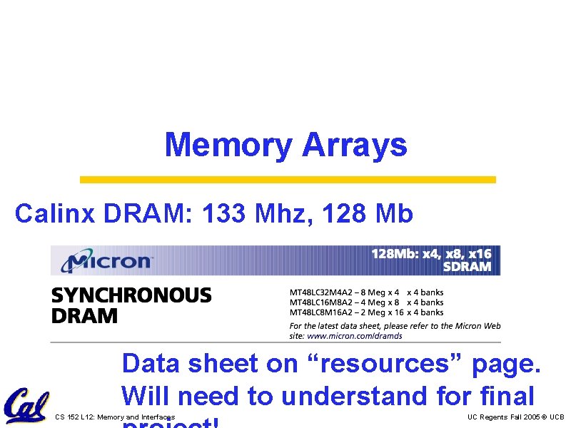
Memory Arrays Calinx DRAM: 133 Mhz, 128 Mb Data sheet on “resources” page. Will need to understand for final CS 152 L 12: Memory and Interfaces UC Regents Fall 2005 © UCB

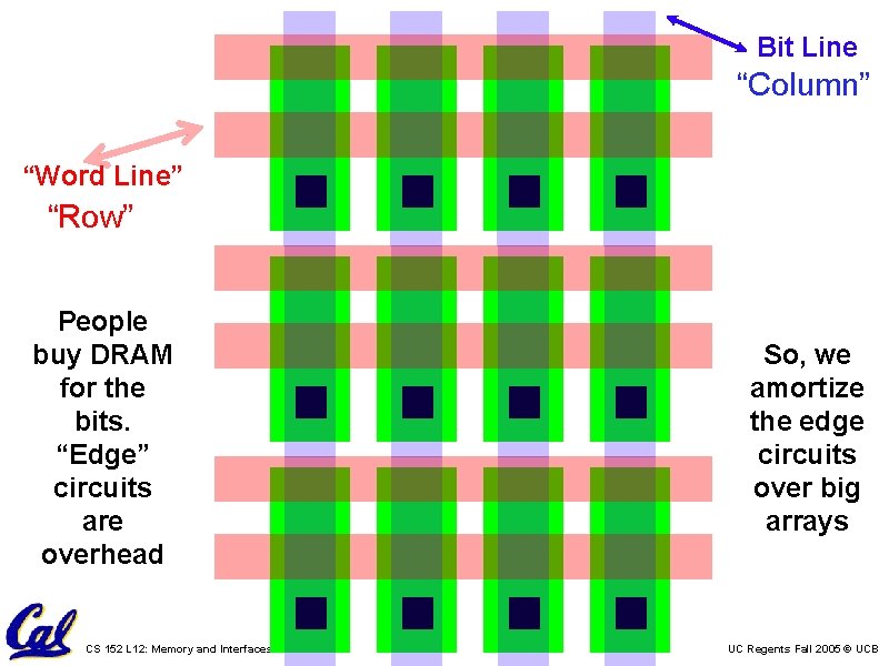
Bit Line “Column” “Word Line” “Row” People buy DRAM for the bits. “Edge” circuits are overhead CS 152 L 12: Memory and Interfaces So, we amortize the edge circuits over big arrays UC Regents Fall 2005 © UCB

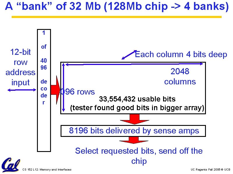
A “bank” of 32 Mb (128 Mb chip -> 4 banks) 1 12 -bit row address input of Each column 4 bits deep 40 96 de co de r 2048 columns 4096 rows 33, 554, 432 usable bits (tester found good bits in bigger array) 8196 bits delivered by sense amps Select requested bits, send off the chip CS 152 L 12: Memory and Interfaces UC Regents Fall 2005 © UCB

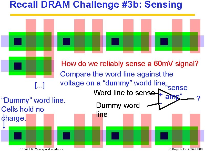
Recall DRAM Challenge #3 b: Sensing How do we reliably sense a 60 m. V signal? Compare the word line against the voltage on a “dummy” world line. [. . . ] “sense Word line to sense + amp” ? “Dummy” word line. Dummy word Cells hold no line charge. CS 152 L 12: Memory and Interfaces UC Regents Fall 2005 © UCB

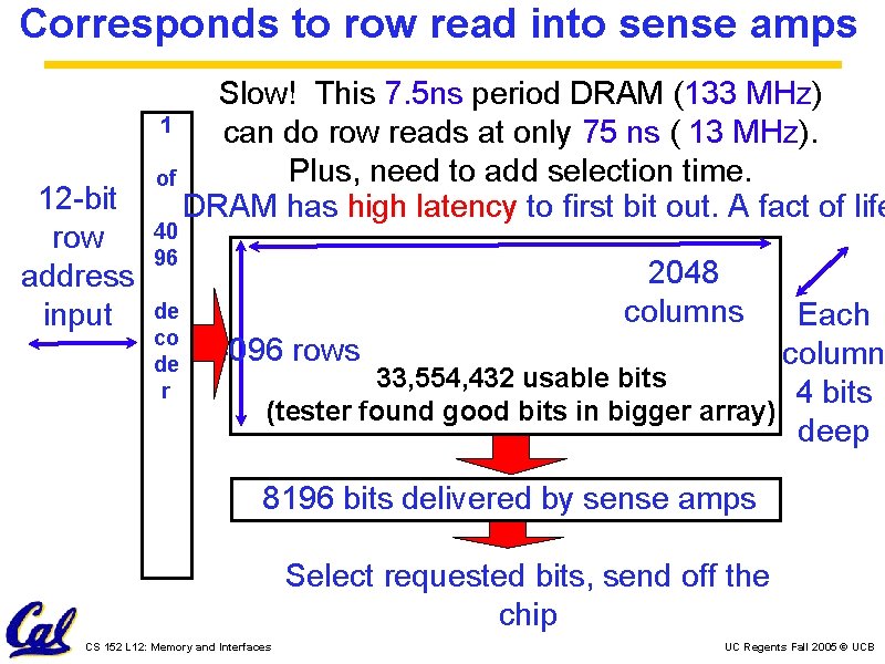
Corresponds to row read into sense amps 12 -bit row address input Slow! This 7. 5 ns period DRAM (133 MHz) 1 can do row reads at only 75 ns ( 13 MHz). Plus, need to add selection time. of DRAM has high latency to first bit out. A fact of life 40 96 de co de r 2048 columns Each 4096 rows column 33, 554, 432 usable bits 4 bits (tester found good bits in bigger array) deep 8196 bits delivered by sense amps Select requested bits, send off the chip CS 152 L 12: Memory and Interfaces UC Regents Fall 2005 © UCB

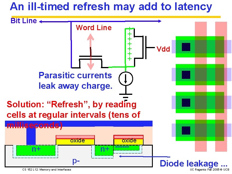
An ill-timed refresh may add to latency Bit Line Word Line + + + + Vdd Parasitic currents leak away charge. Solution: “Refresh”, by reading cells at regular intervals (tens of milliseconds) oxide n+ p. CS 152 L 12: Memory and Interfaces oxide n+ ------ Diode leakage. . . UC Regents Fall 2005 © UCB

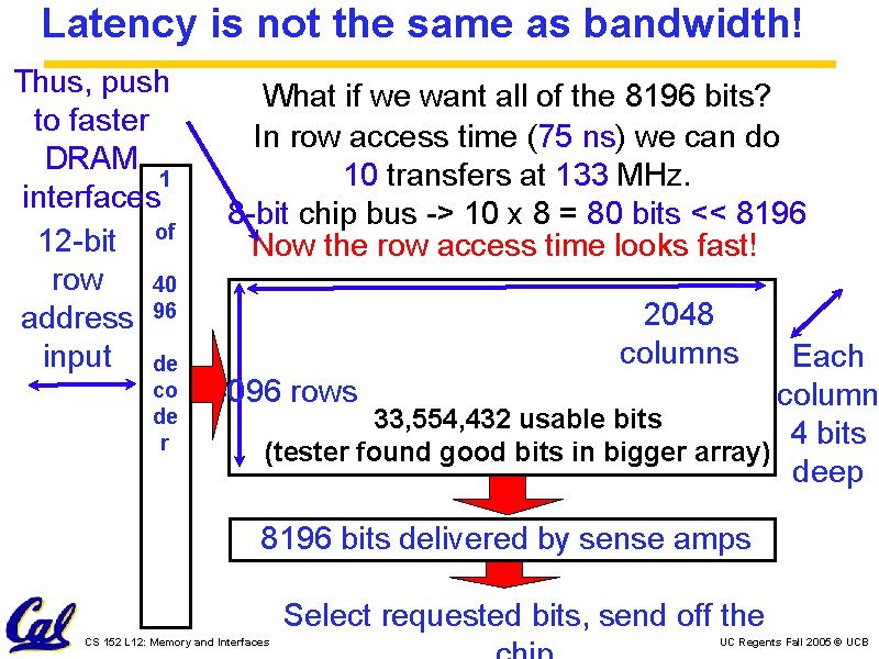
Latency is not the same as bandwidth! Thus, push to faster DRAM 1 interfaces 12 -bit of row 40 address 96 input de co de r What if we want all of the 8196 bits? In row access time (75 ns) we can do 10 transfers at 133 MHz. 8 -bit chip bus -> 10 x 8 = 80 bits << 8196 Now the row access time looks fast! 2048 columns Each 4096 rows column 33, 554, 432 usable bits 4 bits (tester found good bits in bigger array) deep 8196 bits delivered by sense amps Select requested bits, send off the CS 152 L 12: Memory and Interfaces UC Regents Fall 2005 © UCB

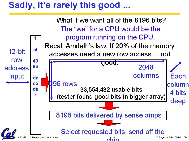
Sadly, it’s rarely this good. . . 1 12 -bit row address input of 40 96 de co de r What if we want all of the 8196 bits? The “we” for a CPU would be the program running on the CPU. Recall Amdalh’s law: If 20% of the memory accesses need a new row access. . . not good. 2048 columns Each 4096 rows column 33, 554, 432 usable bits 4 bits (tester found good bits in bigger array) deep 8196 bits delivered by sense amps Select requested bits, send off the CS 152 L 12: Memory and Interfaces UC Regents Fall 2005 © UCB

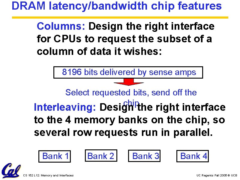
DRAM latency/bandwidth chip features Columns: Design the right interface for CPUs to request the subset of a column of data it wishes: 8196 bits delivered by sense amps Select requested bits, send off the chip Interleaving: Design the right interface to the 4 memory banks on the chip, so several row requests run in parallel. Bank 1 CS 152 L 12: Memory and Interfaces Bank 2 Bank 3 Bank 4 UC Regents Fall 2005 © UCB

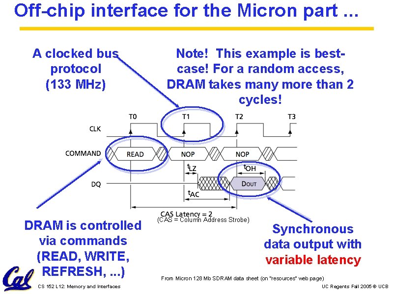
Off-chip interface for the Micron part. . . A clocked bus protocol (133 MHz) DRAM is controlled via commands (READ, WRITE, REFRESH, . . . ) CS 152 L 12: Memory and Interfaces Note! This example is bestcase! For a random access, DRAM takes many more than 2 cycles! (CAS = Column Address Strobe) Synchronous data output with variable latency From Micron 128 Mb SDRAM data sheet (on “resources” web page) UC Regents Fall 2005 © UCB

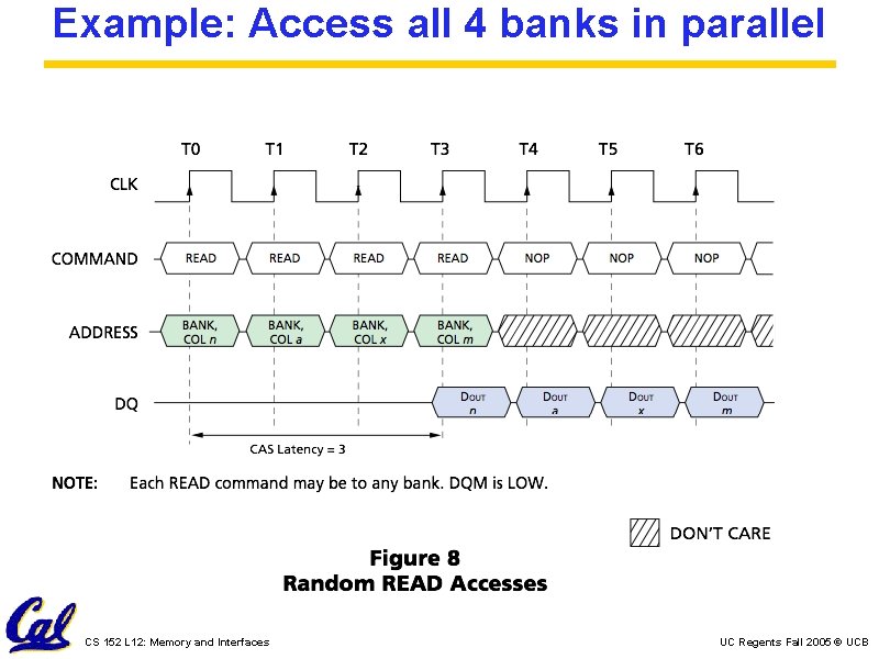
Example: Access all 4 banks in parallel CS 152 L 12: Memory and Interfaces UC Regents Fall 2005 © UCB

Lectures: Coming up next. . . Essential tools for the final project. CS 152 L 12: Memory and Interfaces UC Regents Fall 2005 © UCB