CRU Weekly Meeting Erno DAVID Tivadar KISS Wigner
- Slides: 7

CRU Weekly Meeting Erno DAVID, Tivadar KISS Wigner Research Center for Physics (HU) 13 January, 2016

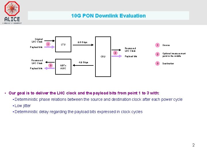
10 G PON Downlink Evaluation Original LHC Clock 1 LTU 9. 6 Gbps Payload bits 2 CRU Recovered LHC Clock Payload bits 4. 8 Gbps 3 1 Source 2 Optional measurement point in the middle 3 Destination Recovered LHC Clock GBTx ASIC • Our goal is to deliver the LHC clock and the payload bits from point 1 to 3 with: • Deterministic phase relations between the source and destination clock after each power cycle • Low jitter • Deterministic delay regarding the payload bits expressed in clock cycles 2

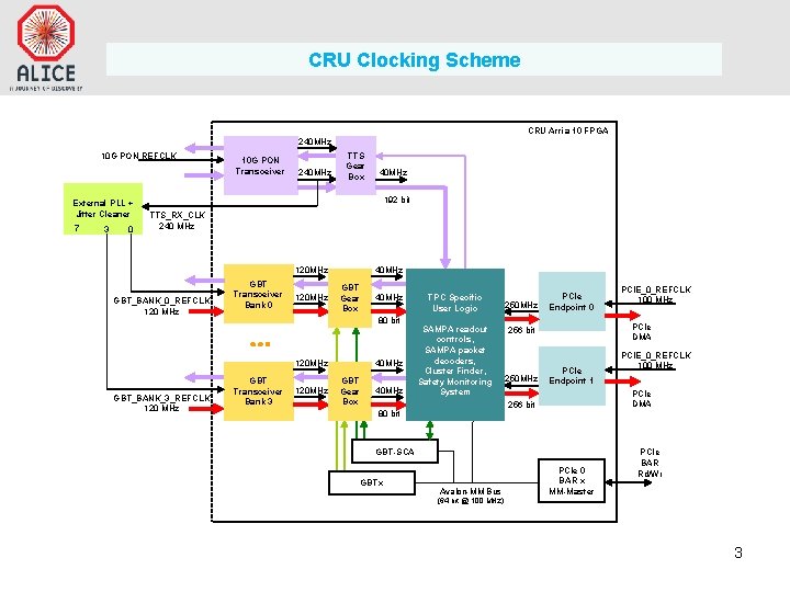
CRU Clocking Scheme CRU Arria 10 FPGA 240 MHz 10 G PON REFCLK External PLL + Jitter Cleaner 7 3 0 10 G PON Transceiver 240 MHz TTS Gear Box 40 MHz 192 bit TTS_RX_CLK 240 MHz 120 MHz GBT_BANK_0_REFCLK 120 MHz GBT Transceiver Bank 0 120 MHz 40 MHz GBT Gear Box 80 bit 120 MHz GBT_BANK_3_REFCLK 120 MHz 40 MHz GBT Transceiver Bank 3 120 MHz 40 MHz GBT Gear Box 40 MHz TPC Specific User Logic SAMPA readout controls, SAMPA packet decoders, Cluster Finder, Safety Monitoring System 250 MHz PCIe Endpoint 0 PCIe DMA 256 bit 250 MHz PCIe Endpoint 1 GBT-SCA GBTx Avalon-MM Bus PCIE_0_REFCLK 100 MHz PCIe DMA 256 bit 80 bit PCIE_0_REFCLK 100 MHz PCIe 0 BAR x MM-Master PCIe BAR Rd/Wr (64 bit @ 100 MHz) 3

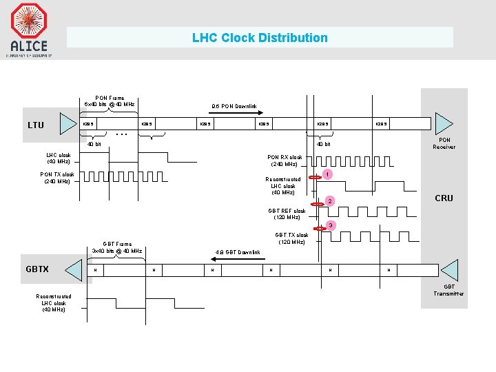
LHC Clock Distribution PON Frame 6 x 40 bits @ 40 MHz LTU K 28. 5 9. 6 PON Downlink K 28. 5 . . . 40 bit PON Receiver 40 bit LHC clock (40 MHz) PON RX clock (240 MHz) PON TX clock (240 MHz) Reconstructed LHC clock (40 MHz) 1 CRU 2 GBT REF clock (120 MHz) 3 GBT TX clock (120 MHz) GBT Frame 3 x 40 bits @ 40 MHz GBTX Reconstructed LHC clock (40 MHz) H 4. 8 GBT Downlink H H H GBT Transmitter

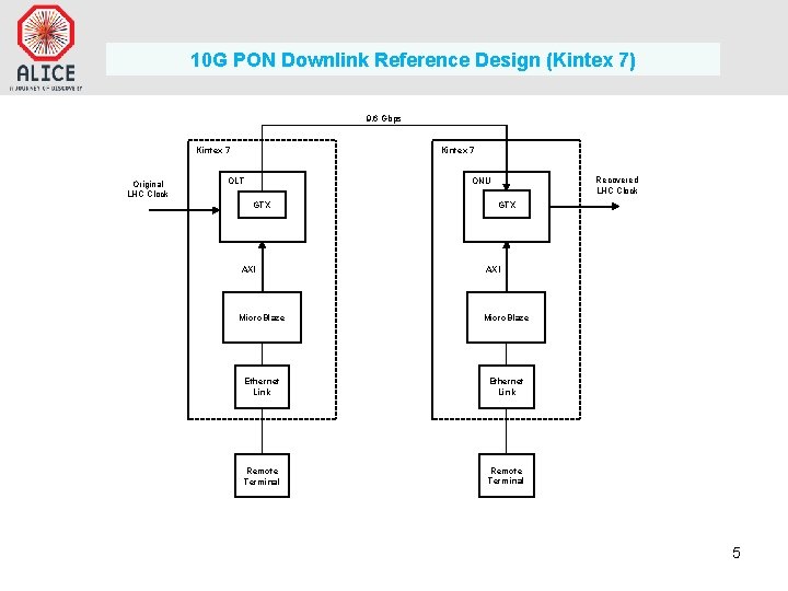
10 G PON Downlink Reference Design (Kintex 7) 9. 6 Gbps Kintex 7 Original LHC Clock Kintex 7 Recovered LHC Clock ONU OLT GTX AXI Micro. Blaze Ethernet Link Remote Terminal 5

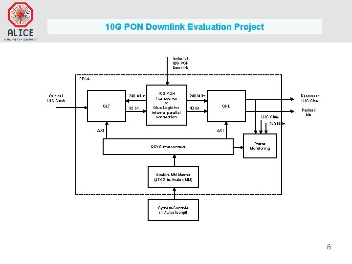
10 G PON Downlink Evaluation Project External 10 G PON Downlink FPGA 240 MHz Original LHC Clock OLT 32 bit 10 G PON Transceiver or Glue Logic for internal parallel connection 240 MHz 40 bit Recovered LHC Clock ONU LHC Clock Payload bits 240 MHz AXI QSYS Interconnect Phase Monitoring Avalon-MM Master (JTAG-to-Avalon-MM) System-Console (TCL test script) 6

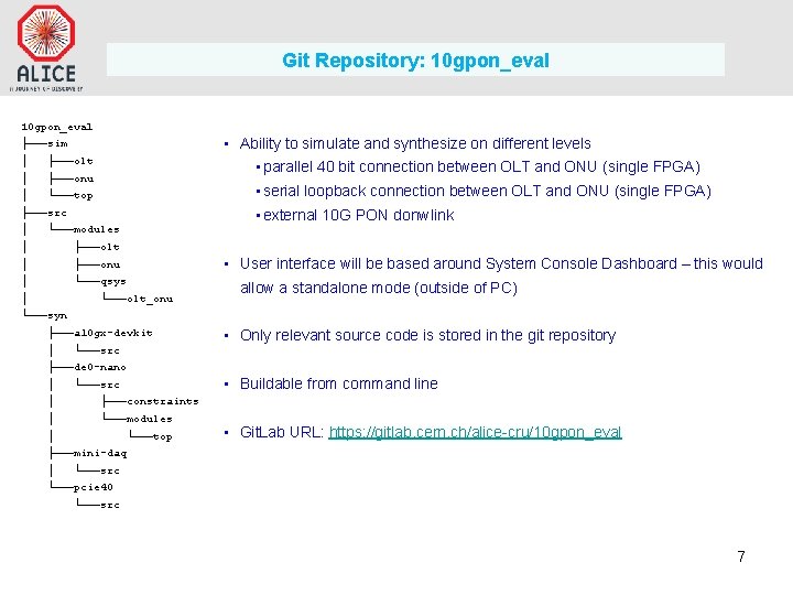
Git Repository: 10 gpon_eval • Ability to simulate and synthesize on different levels ├───sim │ ├───olt │ ├───onu │ └───top • parallel 40 bit connection between OLT and ONU (single FPGA) • serial loopback connection between OLT and ONU (single FPGA) • external 10 G PON donwlink ├───src │ └───modules │ ├───olt │ ├───onu │ └───qsys │ • User interface will be based around System Console Dashboard – this would └───olt_onu allow a standalone mode (outside of PC) └───syn ├───a 10 gx-devkit │ └───src • Only relevant source code is stored in the git repository ├───de 0 -nano │ • Buildable from command line └───src │ ├───constraints │ └───modules │ └───top • Git. Lab URL: https: //gitlab. cern. ch/alice-cru/10 gpon_eval ├───mini-daq │ └───src └───pcie 40 └───src 7