CRU PCIe usage 1 DMA engine firmware sofware
- Slides: 16

CRU PCIe usage 1

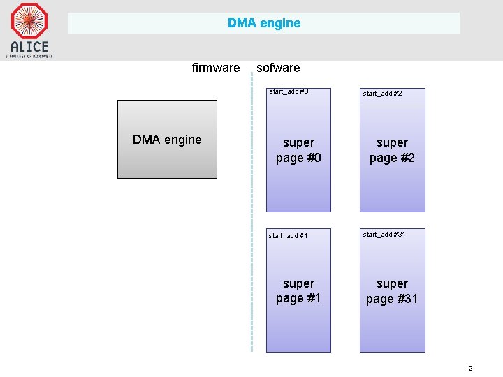
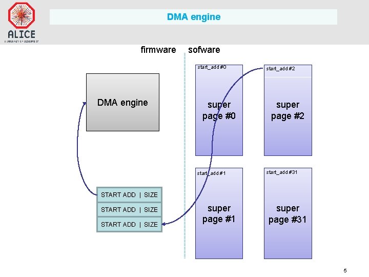
DMA engine firmware sofware start_add #0 DMA engine super page #0 start_add #1 super page #1 start_add #2 super page #2 start_add #31 super page #31 2

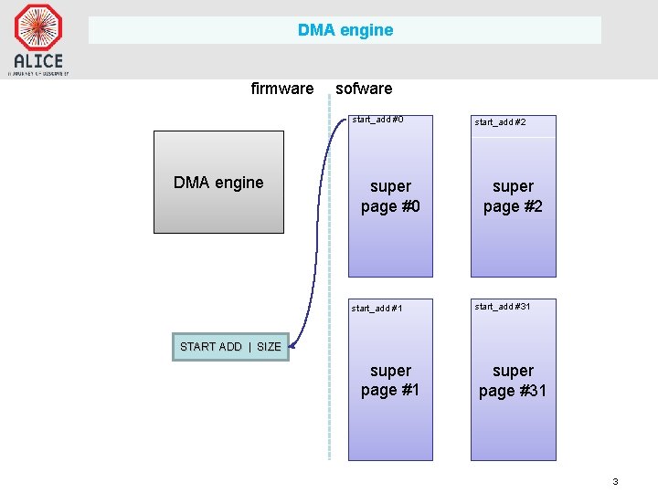
DMA engine firmware sofware start_add #0 DMA engine super page #0 start_add #1 start_add #2 super page #2 start_add #31 START ADD | SIZE super page #1 super page #31 3

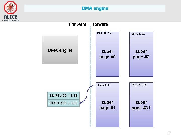
DMA engine firmware sofware start_add #0 DMA engine super page #0 start_add #1 start_add #2 super page #2 start_add #31 START ADD | SIZE super page #1 super page #31 4

DMA engine firmware sofware start_add #0 DMA engine super page #0 start_add #1 start_add #2 super page #2 start_add #31 START ADD | SIZE super page #1 super page #31 5

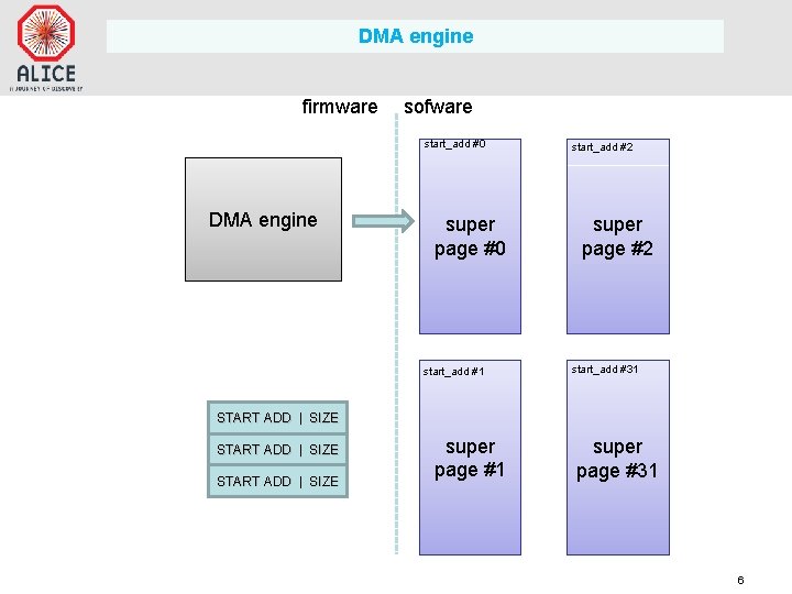
DMA engine firmware sofware start_add #0 DMA engine super page #0 start_add #1 start_add #2 super page #2 start_add #31 START ADD | SIZE super page #1 super page #31 6

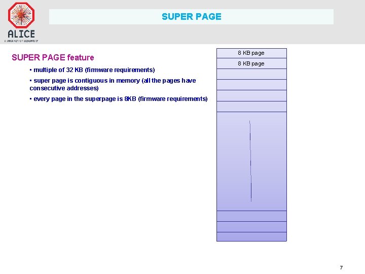
SUPER PAGE feature • multiple of 32 KB (firmware requirements) 8 KB page • super page is contiguous in memory (all the pages have consecutive addresses) • every page in the superpage is 8 KB (firmware requirements) 7

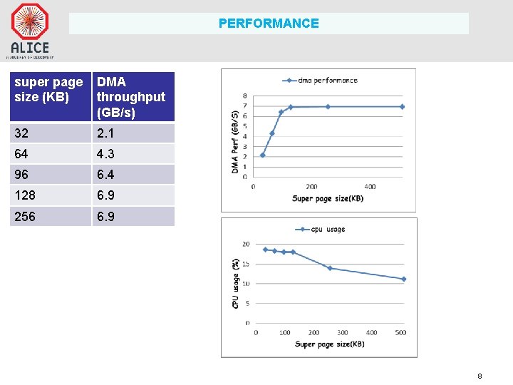
PERFORMANCE super page size (KB) DMA throughput (GB/s) 32 2. 1 64 4. 3 96 6. 4 128 6. 9 256 6. 9 8

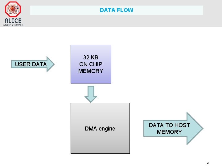
DATA FLOW USER DATA 32 KB ON CHIP MEMORY DMA engine DATA TO HOST MEMORY 9

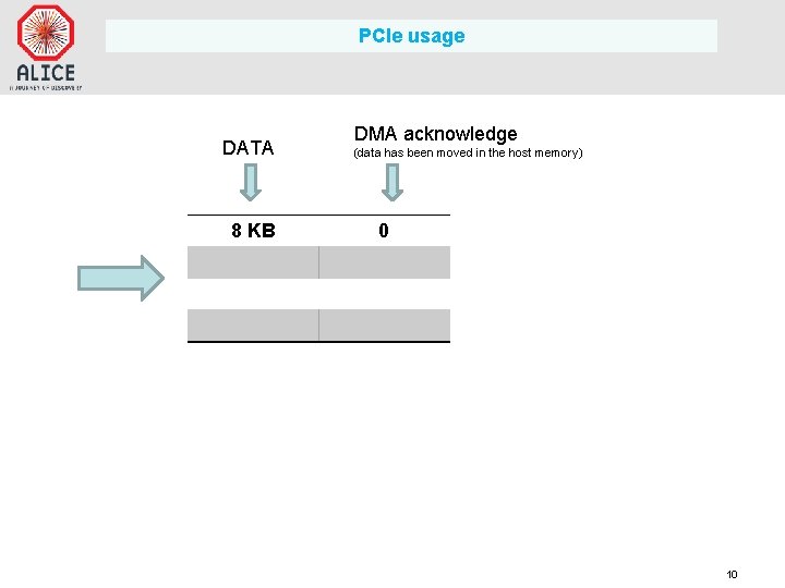
PCIe usage DATA 8 KB DMA acknowledge (data has been moved in the host memory) 0 10

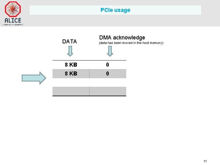
PCIe usage DATA DMA acknowledge (data has been moved in the host memory) 8 KB 0 11

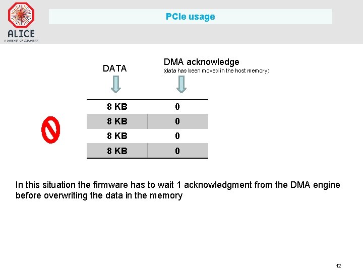
PCIe usage DATA DMA acknowledge (data has been moved in the host memory) 8 KB 0 In this situation the firmware has to wait 1 acknowledgment from the DMA engine before overwriting the data in the memory 12

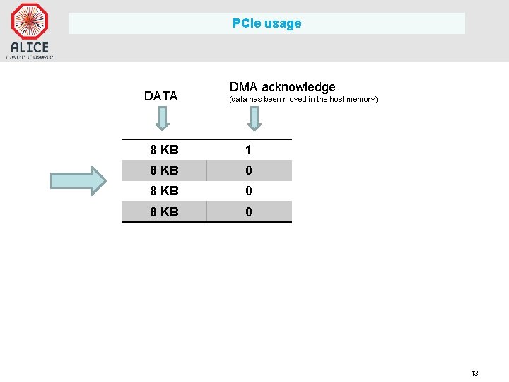
PCIe usage DATA DMA acknowledge (data has been moved in the host memory) 8 KB 1 8 KB 0 13

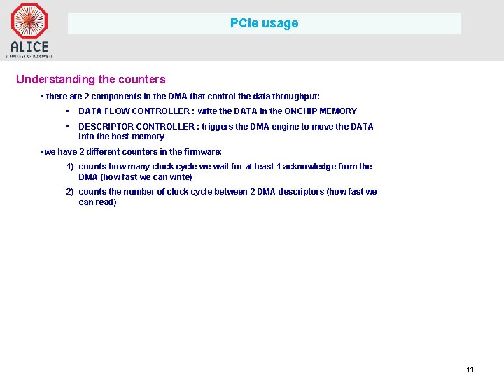
PCIe usage Understanding the counters • there are 2 components in the DMA that control the data throughput: • DATA FLOW CONTROLLER : write the DATA in the ONCHIP MEMORY • DESCRIPTOR CONTROLLER : triggers the DMA engine to move the DATA into the host memory • we have 2 different counters in the firmware: 1) counts how many clock cycle we wait for at least 1 acknowledge from the DMA (how fast we can write) 2) counts the number of clock cycle between 2 DMA descriptors (how fast we can read) 14

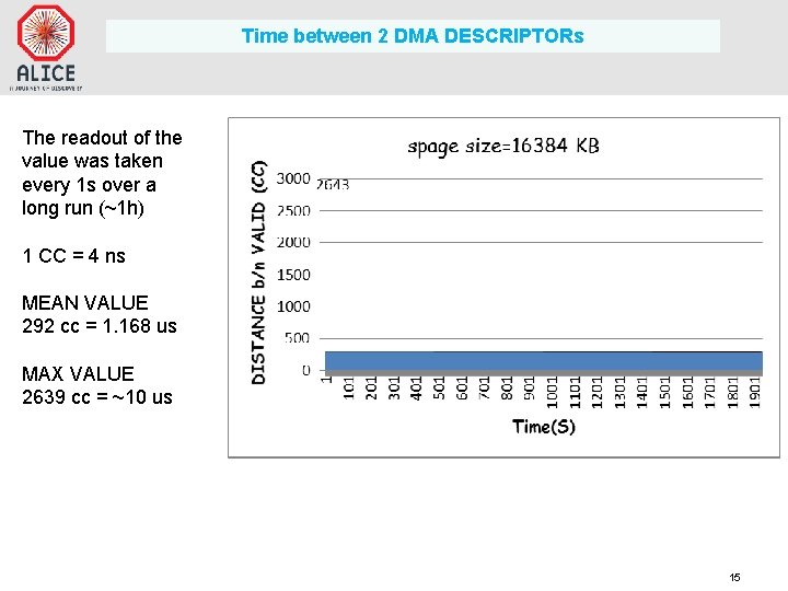
Time between 2 DMA DESCRIPTORs The readout of the value was taken every 1 s over a long run (~1 h) 1 CC = 4 ns MEAN VALUE 292 cc = 1. 168 us MAX VALUE 2639 cc = ~10 us 15

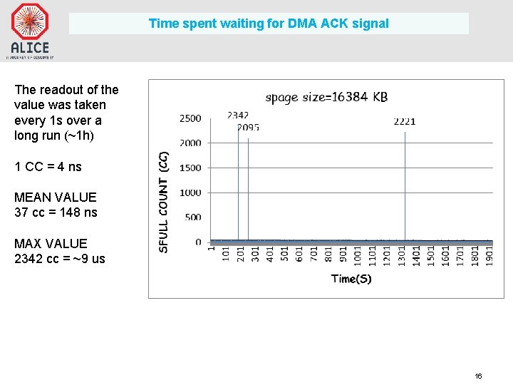
Time spent waiting for DMA ACK signal The readout of the value was taken every 1 s over a long run (~1 h) 1 CC = 4 ns MEAN VALUE 37 cc = 148 ns MAX VALUE 2342 cc = ~9 us 16