CrossTalk Simulation Analysis using HFSS Shravan Kaundinya 1


![References [1] Johnson, Howard W. , and Martin Graham. High-speed digital design: a handbook References [1] Johnson, Howard W. , and Martin Graham. High-speed digital design: a handbook](https://slidetodoc.com/presentation_image_h/314c49c7183804c2cde4e41d64ccebbd/image-18.jpg)
- Slides: 18

Cross-Talk Simulation Analysis using HFSS Shravan Kaundinya 1 3/10/2021 Fall '19 EECS 713 - High-Speed Digital Circuit Design

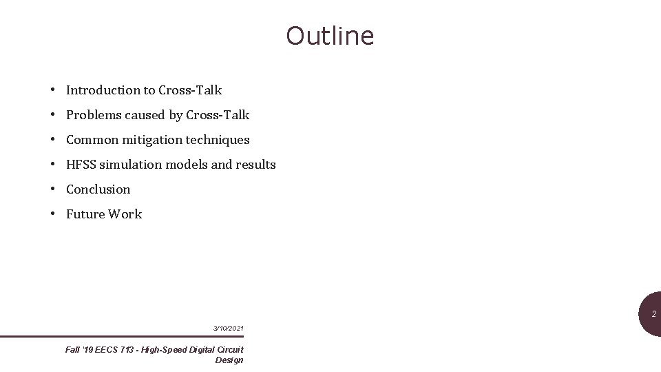
Outline • Introduction to Cross-Talk • Problems caused by Cross-Talk • Common mitigation techniques • HFSS simulation models and results • Conclusion • Future Work 2 3/10/2021 Fall '19 EECS 713 - High-Speed Digital Circuit Design

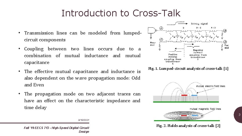
Introduction to Cross-Talk • Transmission lines can be modeled from lumpedcircuit components • Coupling between two lines occurs due to a combination of mutual inductance and mutual capacitance • The effective mutual capacitance and inductance is also dependent on the wave propagation mode: Odd and Even Fig. 1. Lumped-circuit analysis of cross-talk [1] • The propagation mode on two adjacent traces can have an effect on the characteristic impedance and time delay 3 3/10/2021 Fall '19 EECS 713 - High-Speed Digital Circuit Design Fig. 2. Fields analysis of cross-talk [2]

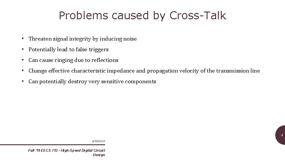
Problems caused by Cross-Talk • Threaten signal integrity by inducing noise • Potentially lead to false triggers • Can cause ringing due to reflections • Change effective characteristic impedance and propagation velocity of the transmission line • Can potentially destroy very sensitive components 4 3/10/2021 Fall '19 EECS 713 - High-Speed Digital Circuit Design

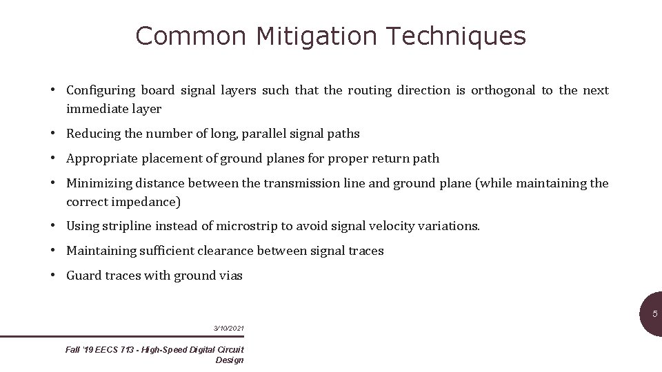
Common Mitigation Techniques • Configuring board signal layers such that the routing direction is orthogonal to the next immediate layer • Reducing the number of long, parallel signal paths • Appropriate placement of ground planes for proper return path • Minimizing distance between the transmission line and ground plane (while maintaining the correct impedance) • Using stripline instead of microstrip to avoid signal velocity variations. • Maintaining sufficient clearance between signal traces • Guard traces with ground vias 5 3/10/2021 Fall '19 EECS 713 - High-Speed Digital Circuit Design

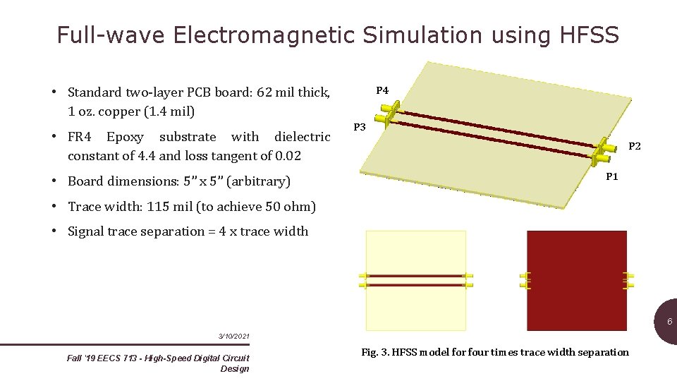
Full-wave Electromagnetic Simulation using HFSS P 4 • Standard two-layer PCB board: 62 mil thick, 1 oz. copper (1. 4 mil) • FR 4 Epoxy substrate with dielectric constant of 4. 4 and loss tangent of 0. 02 • Board dimensions: 5” x 5” (arbitrary) P 3 P 2 P 1 • Trace width: 115 mil (to achieve 50 ohm) • Signal trace separation = 4 x trace width 6 3/10/2021 Fall '19 EECS 713 - High-Speed Digital Circuit Design Fig. 3. HFSS model for four times trace width separation

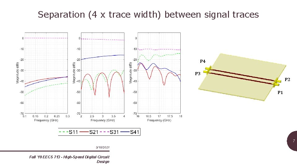
Separation (4 x trace width) between signal traces P 4 P 3 P 2 P 1 7 3/10/2021 Fall '19 EECS 713 - High-Speed Digital Circuit Design

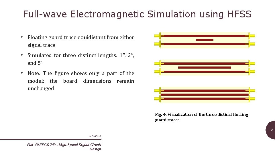
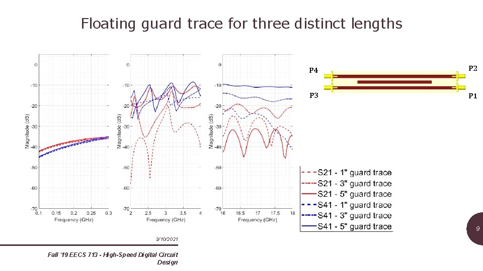
Full-wave Electromagnetic Simulation using HFSS • Floating guard trace equidistant from either signal trace • Simulated for three distinct lengths: 1”, 3”, and 5” • Note: The figure shows only a part of the model; the board dimensions remain unchanged Fig. 4. Visualization of the three distinct floating guard traces 8 3/10/2021 Fall '19 EECS 713 - High-Speed Digital Circuit Design

Floating guard trace for three distinct lengths P 4 P 2 P 3 P 1 9 3/10/2021 Fall '19 EECS 713 - High-Speed Digital Circuit Design

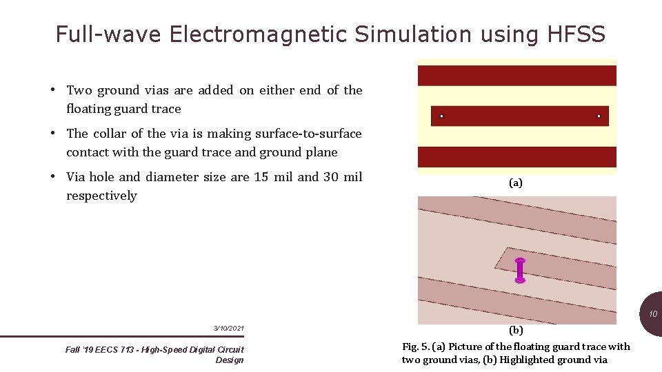
Full-wave Electromagnetic Simulation using HFSS • Two ground vias are added on either end of the floating guard trace • The collar of the via is making surface-to-surface contact with the guard trace and ground plane • Via hole and diameter size are 15 mil and 30 mil respectively (a) 10 3/10/2021 Fall '19 EECS 713 - High-Speed Digital Circuit Design (b) Fig. 5. (a) Picture of the floating guard trace with two ground vias, (b) Highlighted ground via

Floating guard trace with two ground vias P 4 P 2 P 3 P 1 11 3/10/2021 Fall '19 EECS 713 - High-Speed Digital Circuit Design

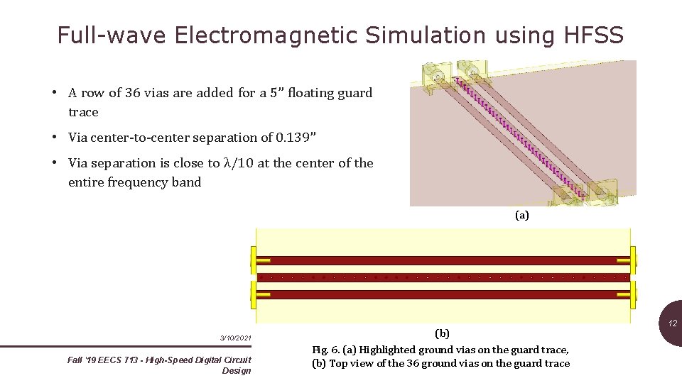
Full-wave Electromagnetic Simulation using HFSS • A row of 36 vias are added for a 5” floating guard trace • Via center-to-center separation of 0. 139” • Via separation is close to λ/10 at the center of the entire frequency band (a) 3/10/2021 Fall '19 EECS 713 - High-Speed Digital Circuit Design (b) Fig. 6. (a) Highlighted ground vias on the guard trace, (b) Top view of the 36 ground vias on the guard trace 12

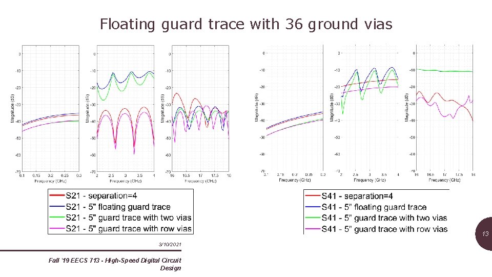
Floating guard trace with 36 ground vias 13 3/10/2021 Fall '19 EECS 713 - High-Speed Digital Circuit Design

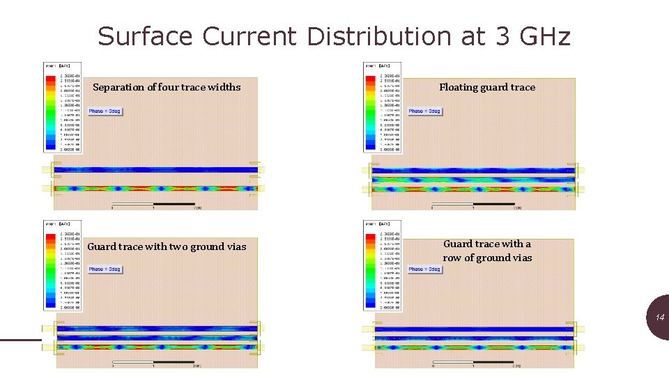
Surface Current Distribution at 3 GHz Separation of four trace widths Floating guard trace Guard trace with two ground vias Guard trace with a row of ground vias 14 3/10/2021 Fall '19 EECS 713 - High-Speed Digital Circuit Design

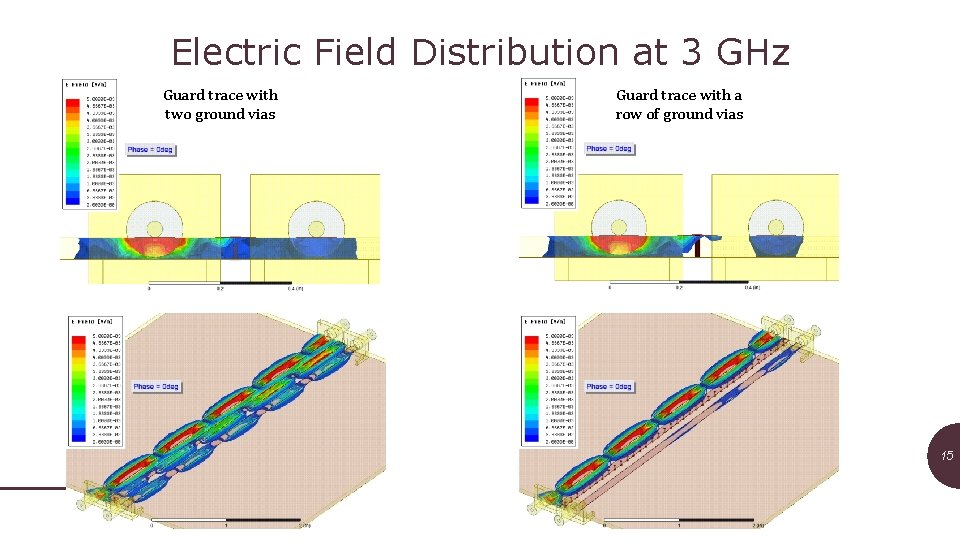
Electric Field Distribution at 3 GHz Guard trace with two ground vias Guard trace with a row of ground vias 15 3/10/2021 Fall '19 EECS 713 - High-Speed Digital Circuit Design

Conclusion • Floating guard trace and guard trace with via do not appear to mitigate cross-talk. On the contrary, they are detrimental to the performance. • Guard trace with a fence of ground vias have almost the same effect as large trace separation. • The usage of guard traces is highly dependent on the board size, signal voltage levels (and power), and frequency of operation. • In general, signal trace separation and continuous ground plane appear to be more favorable than a guard trace for cross-talk mitigation. 16 3/10/2021 Fall '19 EECS 713 - High-Speed Digital Circuit Design

Future work • Investigate the effect of multiple guard traces • Multiple guard traces with varying number of vias • Observe the effect when two or more signal traces are active simultaneously • Fabricate a few designs to validate the simulations • Possibly extend this line of reasoning to stripline architecture 17 3/10/2021 Fall '19 EECS 713 - High-Speed Digital Circuit Design
![References 1 Johnson Howard W and Martin Graham Highspeed digital design a handbook References [1] Johnson, Howard W. , and Martin Graham. High-speed digital design: a handbook](https://slidetodoc.com/presentation_image_h/314c49c7183804c2cde4e41d64ccebbd/image-18.jpg)
References [1] Johnson, Howard W. , and Martin Graham. High-speed digital design: a handbook of black magic. Vol. 155. Upper Saddle River, NJ: Prentice Hall, 1993. [2] Electronics Stack Exchange. https: //electronics. stackexchange. com/questions/233183/pcb-groundpour-crosstalk-and-antennas. Accessed 10 December, 2019. [3] Hall, Stephen H. , Garrett W. Hall, and James A. Mc. Call. High-speed digital system design: a handbook of interconnect theory and design practices. New York: Wiley, 2000. [4] Allen, Chris. “High-Speed Digital Circuit Design, ” EECS 713 Lecture Notes, Fall 2019. www. cresis. ku. edu/~callen/713/EECS 713. htm. [5] Knack, Kella, et al. “Guard Traces: Hit or Myth? ” Altium Resources, 22 July 2019, https: //resources. altium. com/pcb-design-blog/guard-traces-hit-or-myth. 18 3/10/2021 Fall '19 EECS 713 - High-Speed Digital Circuit Design