CROSS FIELD TUBES AND MICROWAVE SEMICONDUCTOR DEVICES BY

CROSS FIELD TUBES AND MICROWAVE SEMICONDUCTOR DEVICES BY: P. Vijaya & M. Niraja
 TED’s are semiconductor devices with no junctions and gates. They")
Transferred Electron Devices (TED) TED’s are semiconductor devices with no junctions and gates. They are fabricated from compound semiconductors like Ga. As, In. P, Cd. Te etc. TED’s operate with hot electrons whose energy is much greater than thermal energy.

Gunn Diode Invented by J. B Gunn

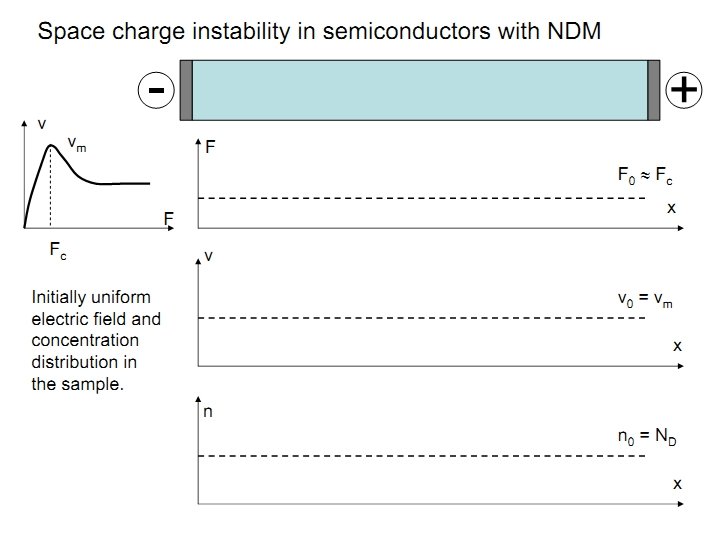
Gunn Effect: Above some critical voltage (Corresponding to Electric field of 2 k-4 k V/cm) the current passing through n-type Ga. As becomes a periodic fluctuating function of time. Frequency of oscillation is determined mainly by the specimen, not by the external circuit. Period of oscillation is inversely proportional to the specimen length and is equal to the transit time of electrons between the electrodes
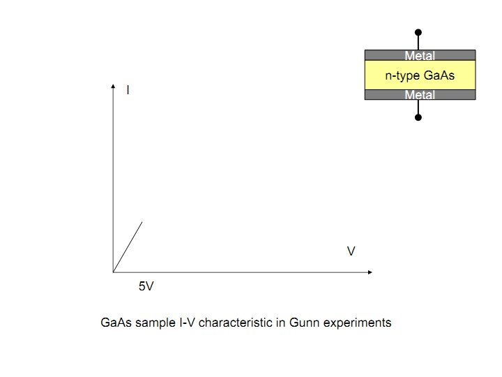
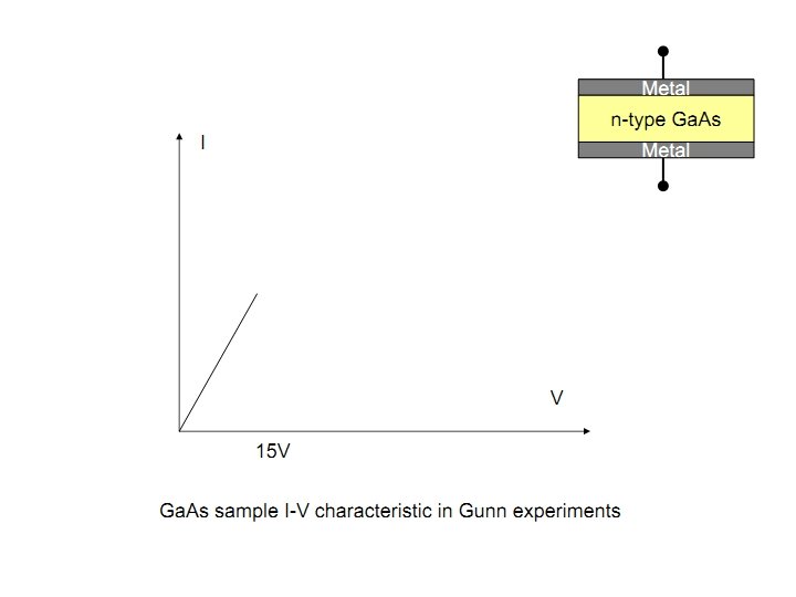
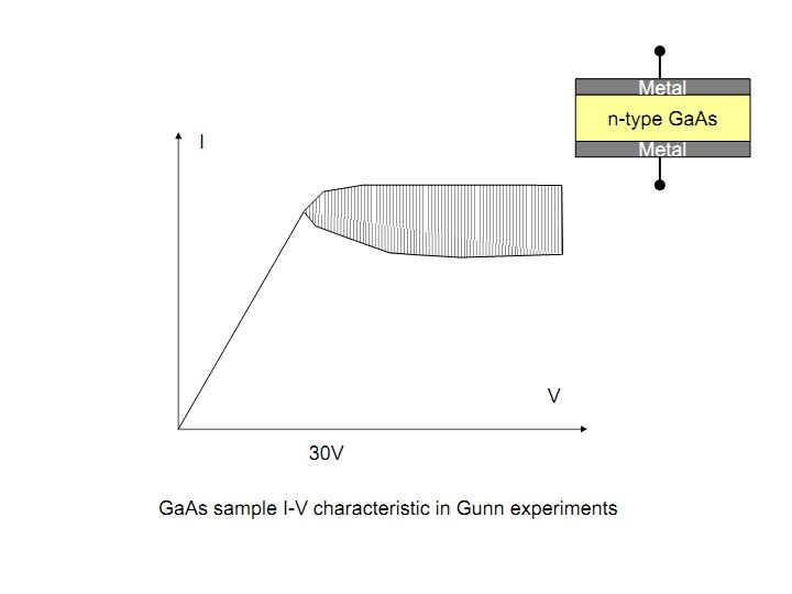

The current waveform was produced by applying a voltage pulse of 16 V and 10 ns duration to an n-type Ga. As of 2. 5 x 10 -3 cm length. The oscillation frequency was 4. 5 Ghz
 Theory Two")
RWH Theory Explanation for Gunn Effect: Ridley – Watkins – Hilsum (RWH) Theory Two concepts related with RWH Theory. ◦ Differential negative resistance ◦ Two valley model

Differential negative resistance Fundamental concept of RWH Theory. Developed in bulk solid state III-V compound when a voltage is applied

Differential negative resistance make the sample electrically unstable.

Two valley model theory

Data for two valleys in Ga. As

Electron transfer mechanism

Conductivity of n-type Ga. As: e = Electron charge μ = Electron mobility = Electron density in the lower valley = Electron density in the upper valley is the electron density
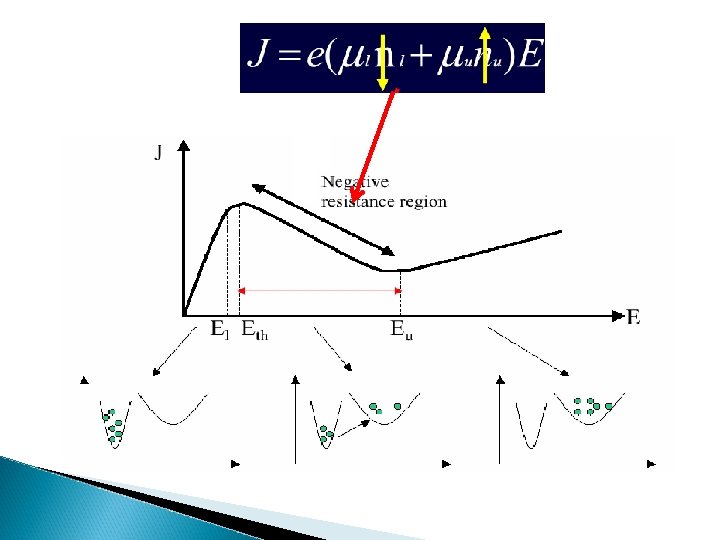

According to RWH theory, in order to exhibit negative resistance the energy band structure of semiconductor should satisfy ◦ The energy difference between two valleys must be several times larger than thermal energy (KT ~ 0. 0259 e. V) ◦ The energy difference between the valleys must be smaller than the bandgap energy (Eg) ◦ Electron in lower valley must have a higher mobility and smaller effective mass than that of in upper valley Possessed by Ga. As, In. P, Cd. Te etc

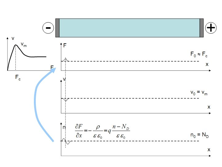
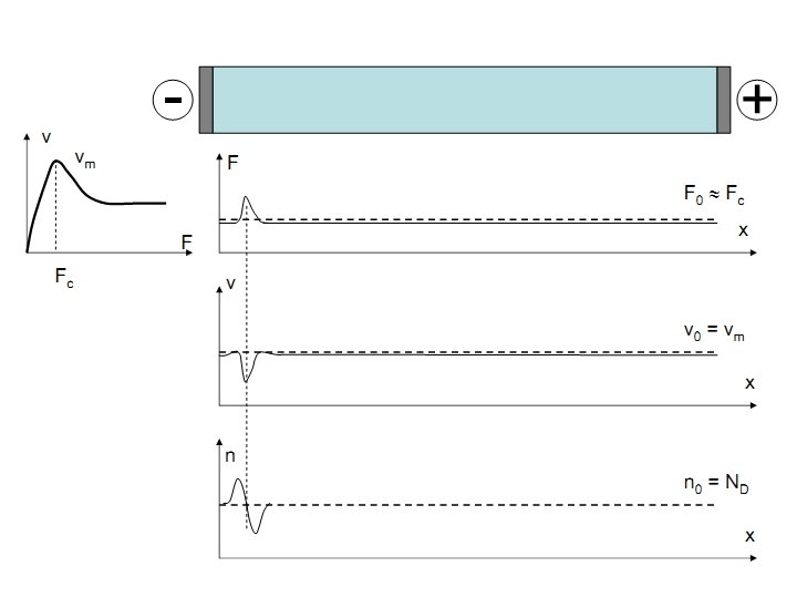
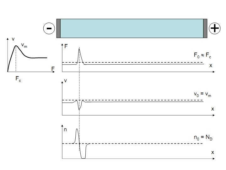
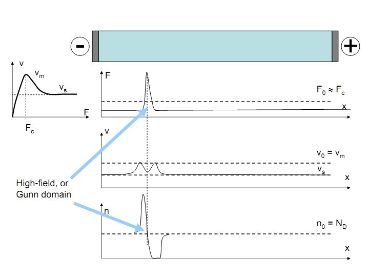
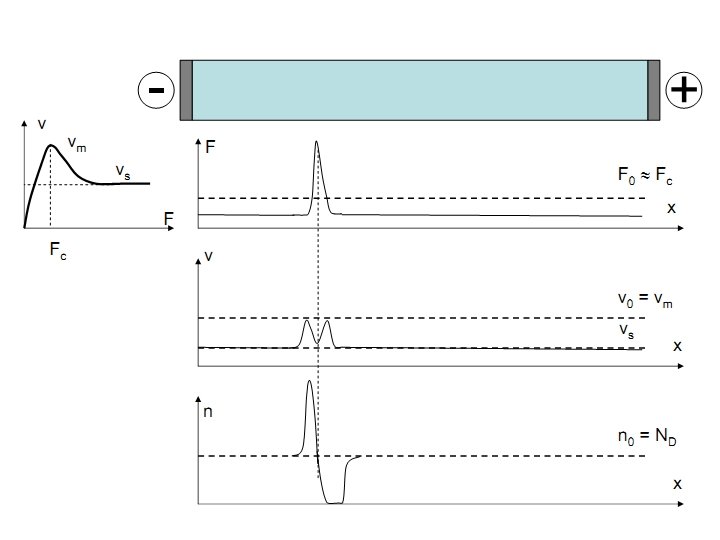
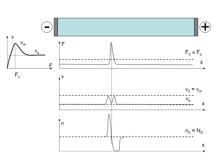
Formation of high field domain In Ga. As, at electric fields exceeding the critical value of Ec ≈ 3. 2 k. V/cm the differential mobility is –ve. When the field exceeds Ec and further increases, the electron drift velocity decreases.
 = 107 cm/s and")
Modes of Operation Gunn Oscillation Mode: ◦ (f x L) = 107 cm/s and (n x L) > 1012 /cm 2 ◦ Cyclic formation of High field domain Stable Amplification Mode ◦ (f x L) = 107 cm/s and 1011/cm 2 < (n x L) >1012/cm 2 LSA Oscillation Mode Bias-circuit ◦ (f x L) >107 cm/s and 2 x 10⁴ < (n/f) > 2 X 10⁵/cm 2 ◦ (f x L) is small. L is very small. When E=Eth current falls as Gunn oscillation begins, leads to oscillation in bias circuit (1 KHz to 100 MHz)
 > Electric relaxation")
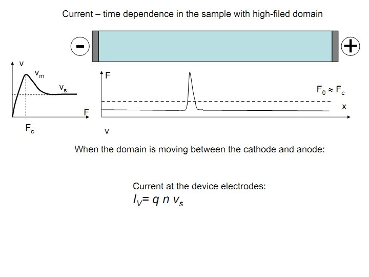
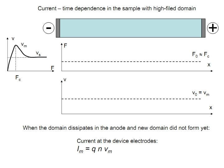
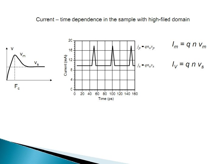
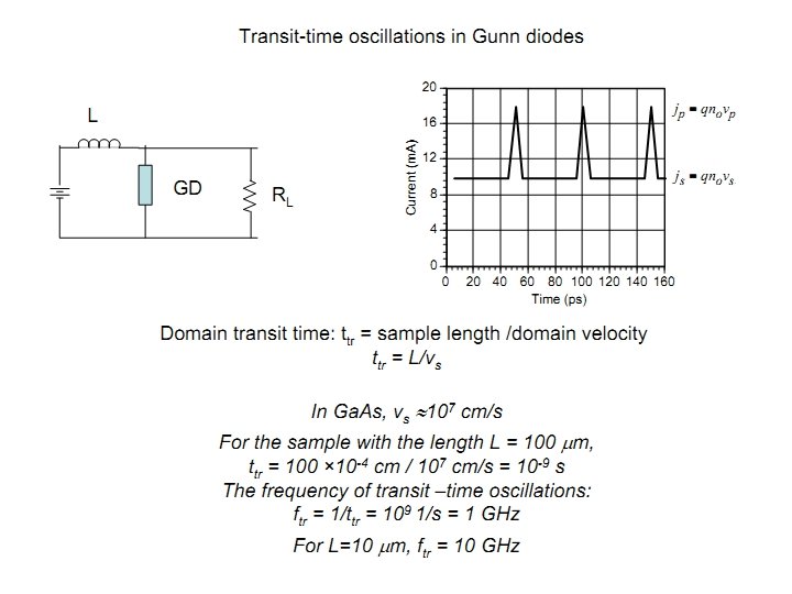
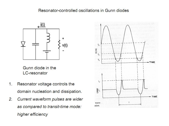
Gunn Oscillation Mode Condition for successful domain drift: Transit time (L/vs) > Electric relaxation time Frequency of oscillation = vdom/Leff. Gunn diode with a resistive circuit -> Voltage change across diode is constant-> Period of oscillation is the time required for the domain to drift from the cathode to anode. Not suitable for microwave applications because of low efficiency. Gunn diode with a resonant circuit has high efficiency.

There are three domain modes for Gunn oscillation modes. 1. Transit time domain mode, (Gunn mode)

2. Delayed domain mode ◦ Here domain is collected while ◦ New domain cannot form until E rises above threshold again. ◦ , ◦ Also called inhibited mode. ◦ Efficiency: 20%

3. Quenched domain mode: ◦ If bias field drops below Es, domain collapses before it reaches anode. ◦ When the bias field swings above Eth, a new domain starts and process repeats. ◦ Frequency of oscillation is determined by resonant circuit. ◦ Efficiency : 13%
 Most Important mode for Gunn oscillator. Domain")
Limited Space charge Accumulation Mode (LSA) Most Important mode for Gunn oscillator. Domain is not allowed to form. Efficiency : 20%
 Gain Bandwidth product")
Gunn Characteristics Power: 1 W (Between 4 HHz and 16 GHz) Gain Bandwidth product : >10 d. B Average gain : 1 – 12 d. B Noise figure : 15 d. B
 and Industrial Telemetry")
Applications of Gunn Diode In radar transmitters Air traffic control (ATC) and Industrial Telemetry Broadband linear amplifier Fast combinational and sequential logic circuit Low and medium power oscillators in microwave receivers As pump sources

In. P Diode

Peak to valley current ratio

Avalanche transit time devices
")
Principle of operation Negative resistance is achieved by creating a delay (1800 Phase shift) between the voltage and current. Delay is achieved by, Delay in generating the avalanche current multiplication Delay due to transit time through the material So called Avalanche transit time (ATT) devices Avalanche is generated by Carrier impact ionization TT is due to the drift in the high field domain
 is")
Features Presence of P-N junctions Diode is reverse biased High field (potential gradient) is applied of the order 400 KV/cm Two modes of ATT ◦ IMPATT- Impact ionization ATT (Efficiency 5 -10%) ◦ TRAPATT- Trapped plasma ATT (Efficiency 20 -60%)
")
Read diode(IMPATT)
")
Read diode (IMPATT)

Read diode is n+ p i p+ diode Avalanche multiplication at p region Intrinsic region acts as the drift space where the generated holes must drift toward p+ Space between n+ p junction and i p+ junction is called the space charge region The device operation delivers power from the dc bias to the oscillation

Operation: ◦ Avalanche multiplication and drift of the high field zone
 and External current Ie(t)")
Carrier current I 0(t) and External current Ie(t)

IMPATT DIode The physical mechanism is the interaction of impact ionization avalanche and the transit time of charge carriers. So Read-type diodes are also called IMPATT diode Most simplest IMPATT diodes are the basic Read diodes Three typical Si IMPATT diodes are shown below. Operations are similar to Read diode

TRAPATT DIOde Derived from IMPATT diode Presence of P-N junctions Diode is reverse biased High current densities than normal avalanche operation It is diode.

Operation:

Parametric Devices

• Uses • non linear reactance or time varying reactance Parametric term is derived from parametric excitation, since the capacitance or inductance, which is a reactive parameter, can be used to produce capacitive or inductive excitation. • Parametric excitation is subdivided into parametric amplification and oscillation. Many of the essential properties of non linear energy storage systems were described by Faraday and Lord Rayleigh. •

• The first analysis of non linear capacitance was given by Van der Ziel in 1948 which suggested that such a device might be useful as a low noise amplifier, since it was essentially a reactive device in which no thermal noise is generated. • In 1949 Landon analyzed and presented experimental results of such circuits used as amplifiers, converters, and oscillators. • In the age of solid state electronics, microwave electronics engineers thought of a solid state microwave device to replace the noisy electron beam amplifier.

• In 1957 Suhl proposed a microwave solid state amplifier that used ferrite. • The first realization of a microwave parametric amplifier was made by Weiss in 1957 after which the parametric amplifier was last discovered. • At present the soild state varactor diode is the most widely used parametric amplifier. • Unlike microwave tubes, transistors and lasers, the parametric diode is of reactive nature and thus generates a very small amount of Johnson (thermal) noise.

• Parametric amplifier utilizes an ac rather than a dc power supply as microwave tubes do. In this respect, the parametric amplifier is analogous to the quantum amplifier laser or maser in which an ac power supply is used.

• A reactance is defined as a circuit element that stores and releases electromagnetic energy as opposed to a resistance, which dissipates energy. • If the stored energy is predominantly in the electric field, the reactance is said to be capacitive; inductive if in the magnetic field. • C = Q/V • If the ratio is not linear, the capacitive reactance is said to be nonlinear. In this case it is convenient to define a non linear capacitance as the partial derivative of charge with respect to voltage.
 = d. Q/dt The analogous definition of non linear inductance is")
i. e C(v) = d. Q/dt The analogous definition of non linear inductance is L(i) = dΦ/di. In the operation of parametric devices, the mixing effects occur when voltages at two or more different frequencies are impressed on a nonlinear reactance.

• Derived a set of general energy relations regarding power flowing into and out of an ideal nonlinear reactance. • These relations are useful in predicting whether power gain is possible in a parametric amplifier.
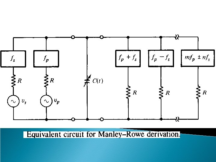

• One signal generator and one pump generator at their respective frequencies , together with associated series resistances and bandpass filters, are applied to a nonlinear capacitance C(t). • These resonating circuits of filters are designed to reject power at all frequencies other than their respective signal frequencies. • In the presence of two applied frequencies an infinite number of resonant frequencies of are generated, where m and n are any integers.

• Each ideal. of the resonating circuits is assumed to be • The power loss by the nonlinear susceptance is negligible. That is the power entering the nonlinear capacitor at the pump frequency is equal to the power leaving the capacitor at the other frequencies through the nonlinear interaction. • Manley and Rowe established the power relations between the input power at the frequencies and the output power at the other frequencies

• It is assumed that the signal voltage vs is much smaller than the pumping voltage vp, and the total voltage across the nonlinear capacitance C(t) is given by • The general expressionof the charge Q deposited on the capacitor is given by

For Q to be real, The total voltage v can be expressed as a function of the charge Q. A similar taylor series expression of v(Q) shows that V to be real,
 is the total derivative of Q w r t")
The current flowing through C(t) is the total derivative of Q w r t time. Hence, Where
 is assumed to be pure reactance, the average")
• Since the capacitance C(t) is assumed to be pure reactance, the average power at the frequencies • is Then conservation of power can be written

Multiply the above equation by a factor of and rearrangement of the resultant into two parts yield Since Then, Becomes, And is independent of ωp or ωs.

For any choice of the frequencies fp and fs, the resonating circuit external to thatof the nonlinear capacitance C(t) can be so adjusted that the currents may keep all the voltage amplitudes Unchanged. The charges are also unchanged, sincethey are functions of the voltages.

Consequently, the frequencies arbitrarily adjusted in order to require Eqn I can be expressed as can be

Since , then Similarly, Where respectively. are replaced by

The above equations are standard forms for the Manley-Rowe power relations. The term indicates the realpower flowing into or leaving the nonlinear capacitor at a frequency of. The frequency represents the fundamental frequency of the pumping voltage oscillator and the frequency signifies the fundamental frequency of the signal voltage generator.

The sign convention for the power term will follow that power flowing into the nonlinear capacitance or the power coming from the two voltage generators is positive, whereas the power leaving from the nonlinear capacitance or the power flowing into the load resistance is negative. Consider for instance, the case where the power output flow is allowed at a frequency of as shown in fig.
- Slides: 74