CPU Design Introduction to Simple Computer Architecture TsungChu
![Instruction Cycle IR←M[AD] Fetch Cycle E x e i le c y cu t Instruction Cycle IR←M[AD] Fetch Cycle E x e i le c y cu t](https://slidetodoc.com/presentation_image_h2/f8ff35ffac5639979df095d2dc9b223c/image-17.jpg)
- Slides: 27

CPU Design -- Introduction to Simple Computer Architecture Tsung-Chu Huang Dept. of Electronic Eng. National Changhua University of Ed. Email: tch@cc. ncue. edu. tw 2005/03/01 CPU Design T. -C. Huang / NCUE Spring 2005 1

Outline Ø Ø Ø CPU Design Introduction to Simple Computer Architecture Instruction Set Architecture Addressing Mode Simple Von Neumann Machine CPU Design Styles T. -C. Huang / NCUE Spring 2005 2

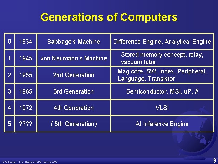
Generations of Computers 0 1834 Babbage’s Machine Difference Engine, Analytical Engine 1 1945 von Neumann’s Machine Stored memory concept, relay, vacuum tube 2 1955 2 nd Generation Mag core, SW, Index, Peripheral, Language, Transistor 3 1965 3 rd Generation Semiconductor, MSI, u. P, // 4 1972 4 th Generation VLSI 5 ? ? ( 5 th Generation) AI Inference Engine CPU Design T. -C. Huang / NCUE Spring 2005 3

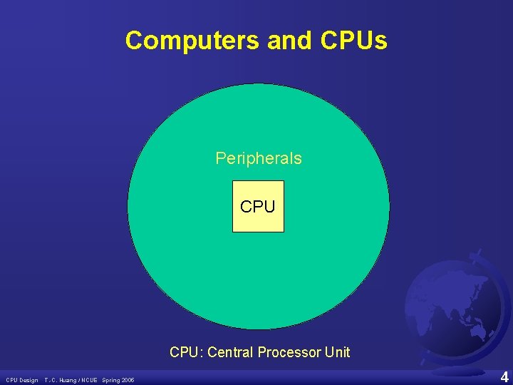
Computers and CPUs Peripherals CPU: Central Processor Unit CPU Design T. -C. Huang / NCUE Spring 2005 4

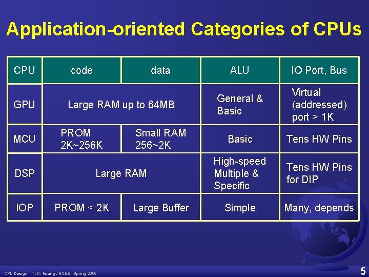
Application-oriented Categories of CPUs CPU GPU MCU DSP IOP CPU Design code data Large RAM up to 64 MB PROM 2 K~256 K Small RAM 256~2 K Large RAM PROM < 2 K T. -C. Huang / NCUE Spring 2005 Large Buffer ALU IO Port, Bus General & Basic Virtual (addressed) port > 1 K Basic Tens HW Pins High-speed Multiple & Specific Tens HW Pins for DIP Simple Many, depends 5

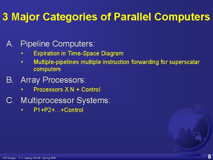
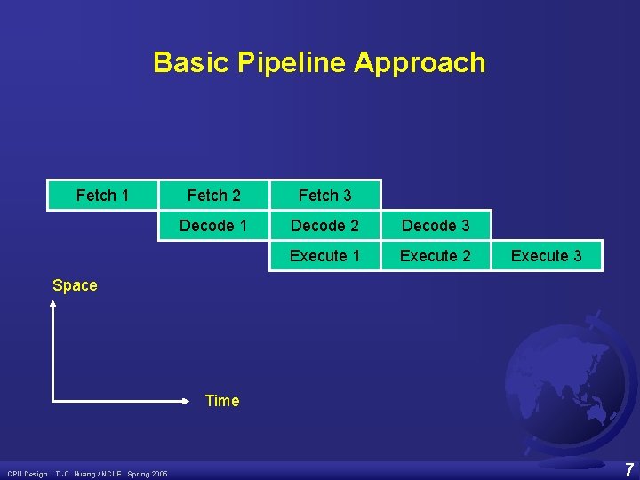
3 Major Categories of Parallel Computers A. Pipeline Computers: • • Expiration in Time-Space Diagram Multiple-pipelines multiple instruction forwarding for superscalar computers B. Array Processors: • Processors X N + Control C. Multiprocessor Systems: • CPU Design P 1+P 2+…+Control T. -C. Huang / NCUE Spring 2005 6

Basic Pipeline Approach Fetch 1 Fetch 2 Fetch 3 Decode 1 Decode 2 Decode 3 Execute 1 Execute 2 Execute 3 Space Time CPU Design T. -C. Huang / NCUE Spring 2005 7

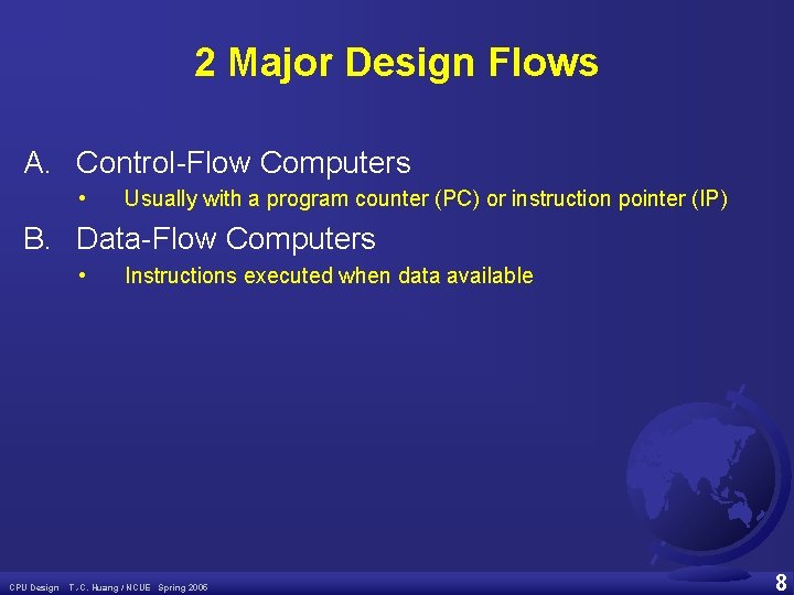
2 Major Design Flows A. Control-Flow Computers • Usually with a program counter (PC) or instruction pointer (IP) B. Data-Flow Computers • CPU Design Instructions executed when data available T. -C. Huang / NCUE Spring 2005 8

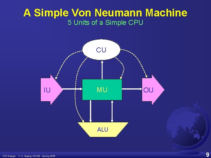
A Simple Von Neumann Machine 5 Units of a Simple CPU CU IU MU OU ALU CPU Design T. -C. Huang / NCUE Spring 2005 9

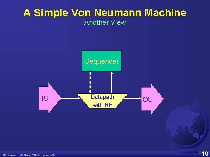
A Simple Von Neumann Machine Another View Sequencer IU CPU Design T. -C. Huang / NCUE Spring 2005 Datapath with RF OU 10

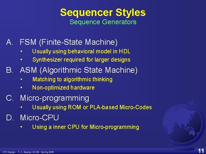
Sequencer Styles Sequence Generators A. FSM (Finite-State Machine) • • Usually using behavioral model in HDL Synthesizer required for larger designs B. ASM (Algorithmic State Machine) • • Matching to algorithmic thinking Non-optimized hardware C. Micro-programming • Usually using ROM or PLA-based Micro-Codes D. Micro-CPU • CPU Design Using a inner CPU for Micro-programming T. -C. Huang / NCUE Spring 2005 11

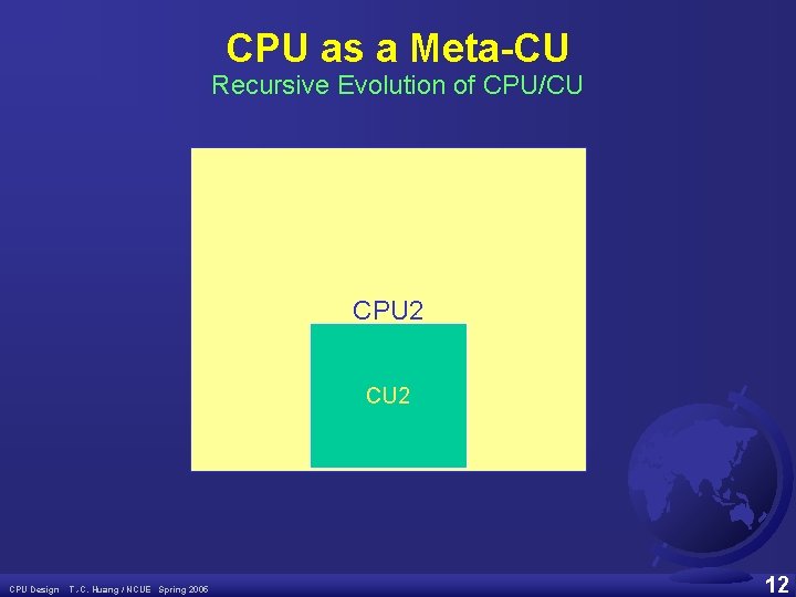
CPU as a Meta-CU Recursive Evolution of CPU/CU CPU 2 CPU 1 CPU Design T. -C. Huang / NCUE Spring 2005 12

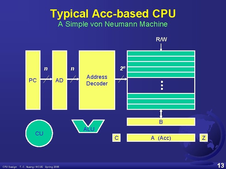
Typical Acc-based CPU A Simple von Neumann Machine R/W n PC n AD 2 n Address Decoder B CU CPU Design T. -C. Huang / NCUE Spring 2005 ALU C A (Acc) Z 13

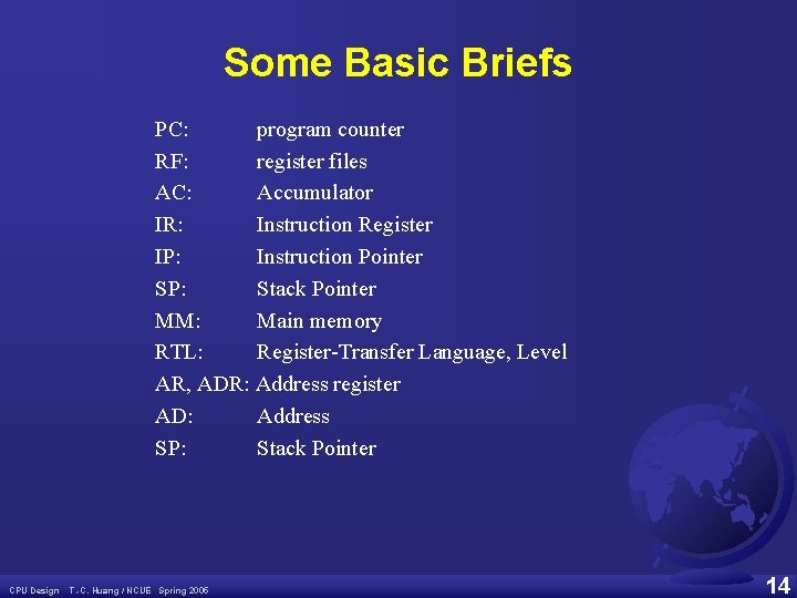
Some Basic Briefs PC: program counter RF: register files AC: Accumulator IR: Instruction Register IP: Instruction Pointer SP: Stack Pointer MM: Main memory RTL: Register-Transfer Language, Level AR, ADR: Address register AD: Address SP: Stack Pointer CPU Design T. -C. Huang / NCUE Spring 2005 14

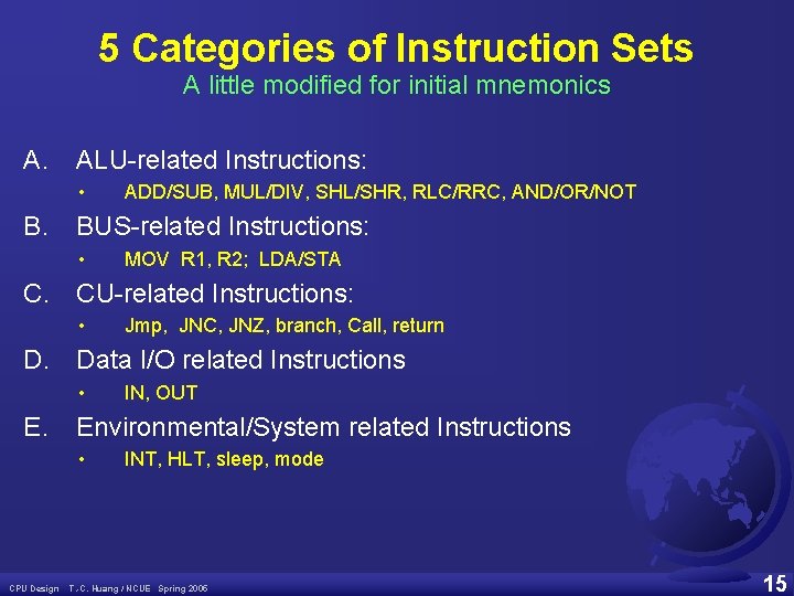
5 Categories of Instruction Sets A little modified for initial mnemonics A. ALU-related Instructions: • B. ADD/SUB, MUL/DIV, SHL/SHR, RLC/RRC, AND/OR/NOT BUS-related Instructions: • MOV R 1, R 2; LDA/STA C. CU-related Instructions: • Jmp, JNC, JNZ, branch, Call, return D. Data I/O related Instructions • E. Environmental/System related Instructions • CPU Design IN, OUT INT, HLT, sleep, mode T. -C. Huang / NCUE Spring 2005 15

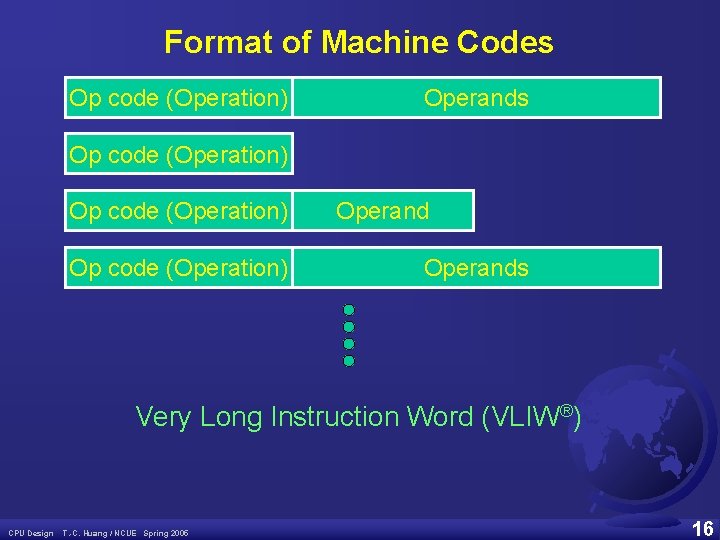
Format of Machine Codes Op code (Operation) Operands Op code (Operation) Operands Very Long Instruction Word (VLIW®) CPU Design T. -C. Huang / NCUE Spring 2005 16
![Instruction Cycle IRMAD Fetch Cycle E x e i le c y cu t Instruction Cycle IR←M[AD] Fetch Cycle E x e i le c y cu t](https://slidetodoc.com/presentation_image_h2/f8ff35ffac5639979df095d2dc9b223c/image-17.jpg)
Instruction Cycle IR←M[AD] Fetch Cycle E x e i le c y cu t D o c e de C C on T. -C. Huang / NCUE Spring 2005 e CPU Design yc l case(IR) PC←PC+1 AD←PC R 1←R 2□R 3 17

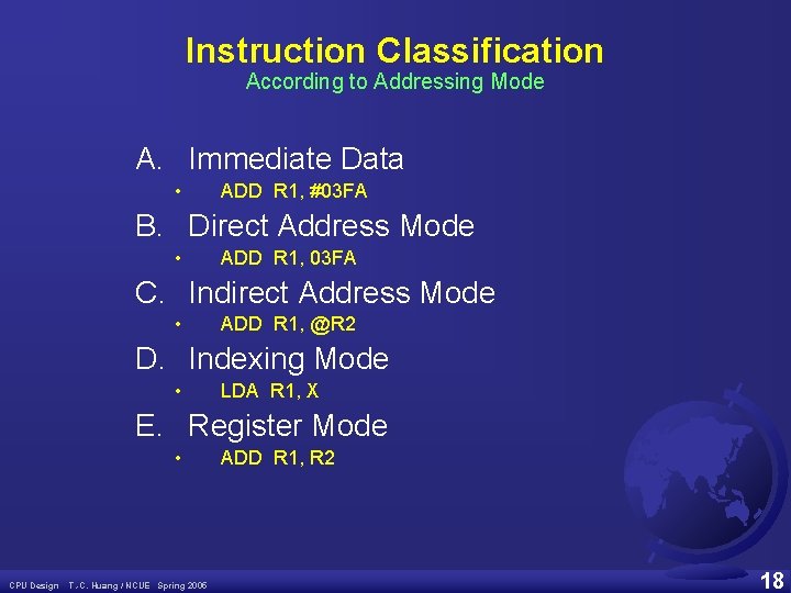
Instruction Classification According to Addressing Mode A. Immediate Data • ADD R 1, #03 FA B. Direct Address Mode • ADD R 1, 03 FA C. Indirect Address Mode • ADD R 1, @R 2 D. Indexing Mode • LDA R 1, X E. Register Mode • CPU Design T. -C. Huang / NCUE Spring 2005 ADD R 1, R 2 18

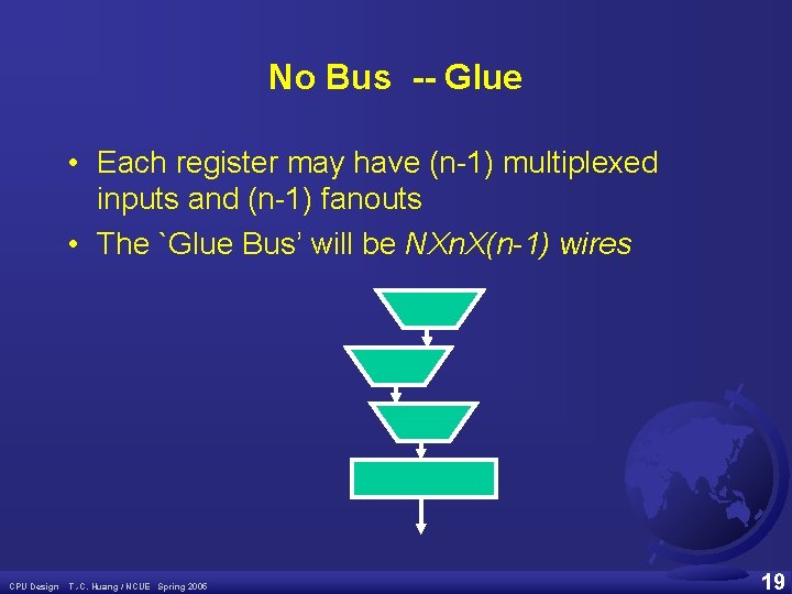
No Bus -- Glue • Each register may have (n-1) multiplexed inputs and (n-1) fanouts • The `Glue Bus’ will be NXn. X(n-1) wires CPU Design T. -C. Huang / NCUE Spring 2005 19

With Bus • Look Bus as a Register in ASM Design • To prevent from Bus Contention, switch at outputs • At a time, only one Write, multiple Read • B mnemonic can be used as a Buffer/Bus CPU Design T. -C. Huang / NCUE Spring 2005 20

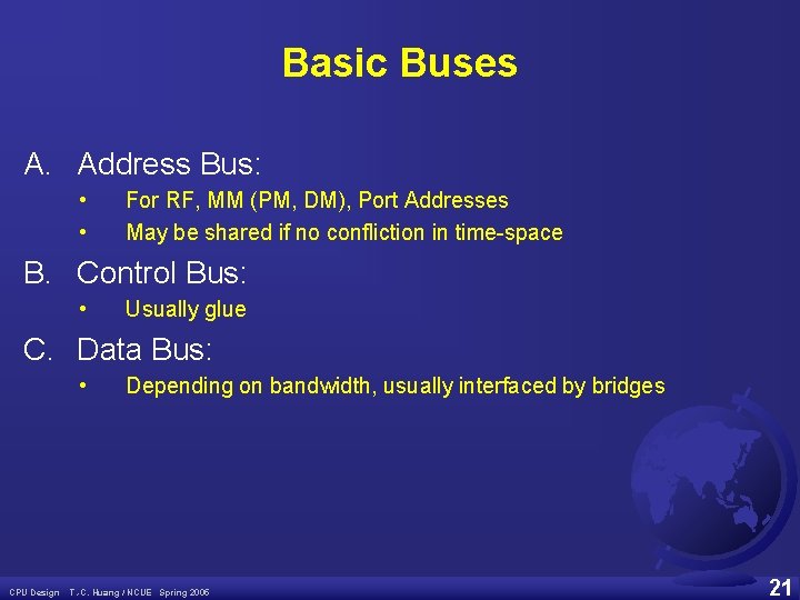
Basic Buses A. Address Bus: • • For RF, MM (PM, DM), Port Addresses May be shared if no confliction in time-space B. Control Bus: • Usually glue C. Data Bus: • CPU Design Depending on bandwidth, usually interfaced by bridges T. -C. Huang / NCUE Spring 2005 21

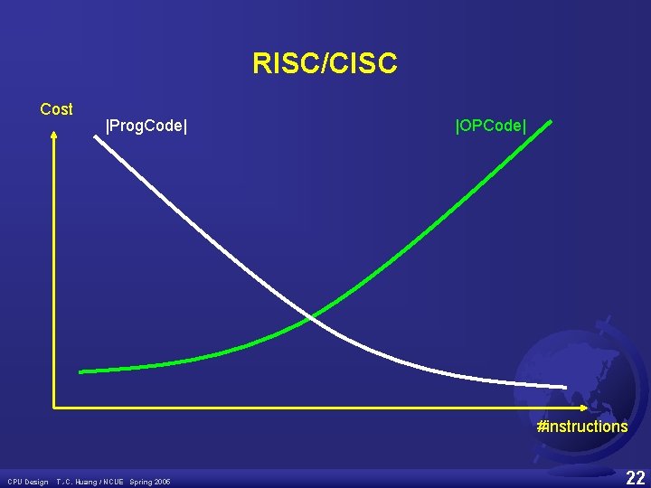
RISC/CISC Cost |Prog. Code| |OPCode| #instructions CPU Design T. -C. Huang / NCUE Spring 2005 22

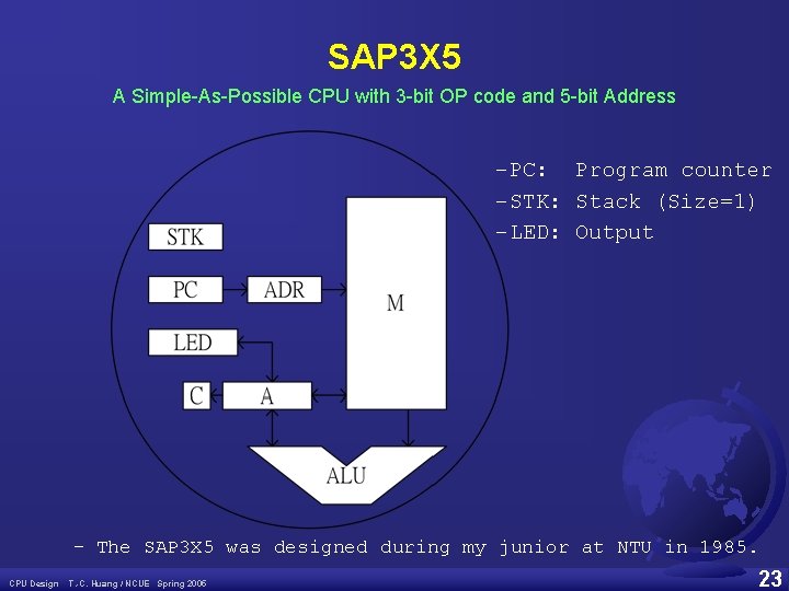
SAP 3 X 5 A Simple-As-Possible CPU with 3 -bit OP code and 5 -bit Address –PC: Program counter –STK: Stack (Size=1) –LED: Output – The SAP 3 X 5 was designed during my junior at NTU in 1985. CPU Design T. -C. Huang / NCUE Spring 2005 23

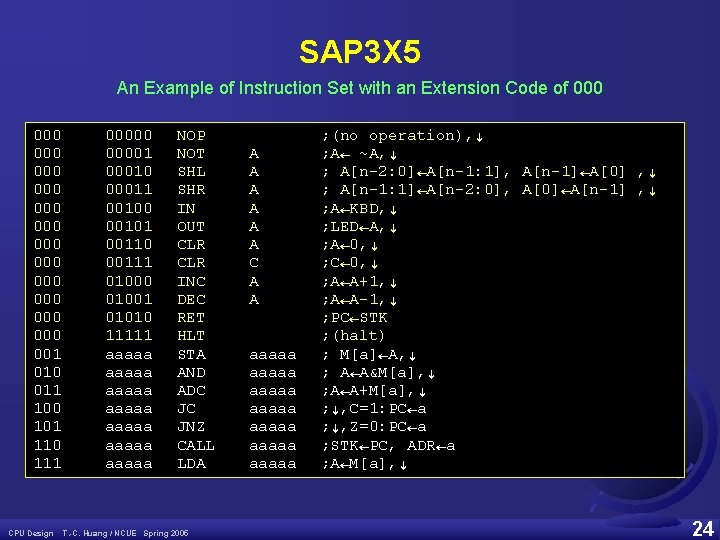
SAP 3 X 5 An Example of Instruction Set with an Extension Code of 000 000 000 000 001 010 011 100 101 110 111 CPU Design 000001 00010 00011 00100 00101 00110 00111 01000 01001 01010 11111 aaaaa aaaaa NOP NOT SHL SHR IN OUT CLR INC DEC RET HLT STA AND ADC JC JNZ CALL LDA T. -C. Huang / NCUE Spring 2005 A A A C A A aaaaa aaaaa ; (no operation), ↓ ; A← ~A, ↓ ; A[n-2: 0]←A[n-1: 1], A[n-1]←A[0] , ↓ ; A[n-1: 1]←A[n-2: 0], A[0]←A[n-1] , ↓ ; A←KBD, ↓ ; LED←A, ↓ ; A← 0, ↓ ; C← 0, ↓ ; A←A+1, ↓ ; A←A-1, ↓ ; PC←STK ; (halt) ; M[a]←A, ↓ ; A←A&M[a], ↓ ; A←A+M[a], ↓ ; ↓, C=1: PC←a ; ↓, Z=0: PC←a ; STK←PC, ADR←a ; A←M[a], ↓ 24

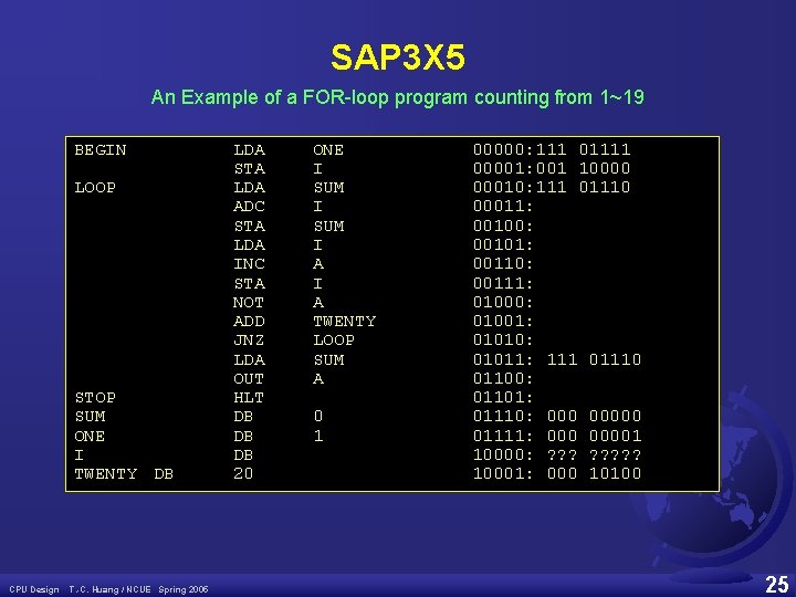
SAP 3 X 5 An Example of a FOR-loop program counting from 1~19 BEGIN LOOP STOP SUM ONE I TWENTY DB CPU Design T. -C. Huang / NCUE Spring 2005 LDA STA LDA ADC STA LDA INC STA NOT ADD JNZ LDA OUT HLT DB DB DB 20 ONE I SUM I A TWENTY LOOP SUM A 0 1 00000: 111 01111 00001: 001 10000 00010: 111 01110 00011: 00100: 00101: 00110: 00111: 01000: 01001: 01010: 01011: 111 01110 01100: 01101: 01110: 00000 01111: 00001 10000: ? ? ? ? 10001: 000 10100 25

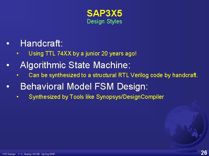
SAP 3 X 5 Design Styles • Handcraft: • • Algorithmic State Machine: • • Can be synthesized to a structural RTL Verilog code by handcraft. Behavioral Model FSM Design: • CPU Design Using TTL 74 XX by a junior 20 years ago! Synthesized by Tools like Synopsys/Design. Compiler T. -C. Huang / NCUE Spring 2005 26

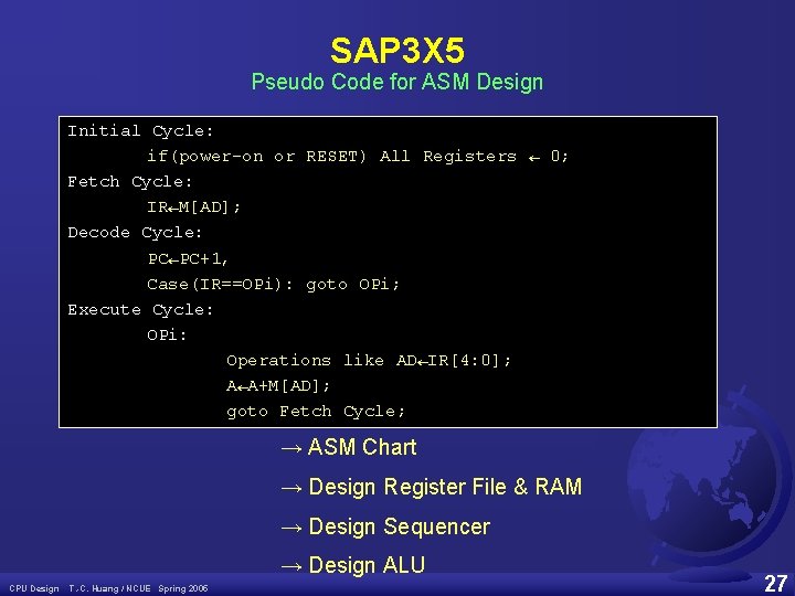
SAP 3 X 5 Pseudo Code for ASM Design Initial Cycle: if(power-on or RESET) All Registers ← 0; Fetch Cycle: IR←M[AD]; Decode Cycle: PC←PC+1, Case(IR==OPi): goto OPi; Execute Cycle: OPi: Operations like AD←IR[4: 0]; A←A+M[AD]; goto Fetch Cycle; → ASM Chart → Design Register File & RAM → Design Sequencer → Design ALU CPU Design T. -C. Huang / NCUE Spring 2005 27