Cpr E 281 Digital Logic Instructor Alexander Stoytchev


![A shifter circuit [ Figure 4. 50 from the textbook ] A shifter circuit [ Figure 4. 50 from the textbook ]](https://slidetodoc.com/presentation_image_h2/7398568bfce903c5f4ff709b4e0a69cc/image-5.jpg)
![A barrel shifter circuit [ Figure 4. 51 from the textbook ] A barrel shifter circuit [ Figure 4. 51 from the textbook ]](https://slidetodoc.com/presentation_image_h2/7398568bfce903c5f4ff709b4e0a69cc/image-6.jpg)

![A simple memory element A B [ Figure 5. 2 from the textbook ] A simple memory element A B [ Figure 5. 2 from the textbook ]](https://slidetodoc.com/presentation_image_h2/7398568bfce903c5f4ff709b4e0a69cc/image-14.jpg)
![A Strange Loop [http: //animalsiadmire. blogspot. com/2011/07/stupid-snake-eating-itself. html] A Strange Loop [http: //animalsiadmire. blogspot. com/2011/07/stupid-snake-eating-itself. html]](https://slidetodoc.com/presentation_image_h2/7398568bfce903c5f4ff709b4e0a69cc/image-16.jpg)




![The Basic Latch Q [ Figure 5. 3 from the textbook ] The Basic Latch Q [ Figure 5. 3 from the textbook ]](https://slidetodoc.com/presentation_image_h2/7398568bfce903c5f4ff709b4e0a69cc/image-41.jpg)




![Single Pole, Double Throw = SPDT [http: //electronicsclub. info/images/swabc. gif] Single Pole, Double Throw = SPDT [http: //electronicsclub. info/images/swabc. gif]](https://slidetodoc.com/presentation_image_h2/7398568bfce903c5f4ff709b4e0a69cc/image-96.jpg)
![Single Pole, Double Throw = SPDT [http: //www. cubisteffects. com/images/MIY/Pt 3_Throw. jpg] Single Pole, Double Throw = SPDT [http: //www. cubisteffects. com/images/MIY/Pt 3_Throw. jpg]](https://slidetodoc.com/presentation_image_h2/7398568bfce903c5f4ff709b4e0a69cc/image-97.jpg)

![A Simple Circuit [ Platt 2009 ] A Simple Circuit [ Platt 2009 ]](https://slidetodoc.com/presentation_image_h2/7398568bfce903c5f4ff709b4e0a69cc/image-101.jpg)
![Let’s Take a Closer Look at This [ Platt 2009 ] Let’s Take a Closer Look at This [ Platt 2009 ]](https://slidetodoc.com/presentation_image_h2/7398568bfce903c5f4ff709b4e0a69cc/image-102.jpg)
![A Similar Example with NAND Gates [ Platt 2009 ] A Similar Example with NAND Gates [ Platt 2009 ]](https://slidetodoc.com/presentation_image_h2/7398568bfce903c5f4ff709b4e0a69cc/image-103.jpg)


- Slides: 105

Cpr. E 281: Digital Logic Instructor: Alexander Stoytchev http: //www. ece. iastate. edu/~alexs/classes/

Latches Cpr. E 281: Digital Logic Iowa State University, Ames, IA Copyright © Alexander Stoytchev

Administrative Stuff • HW 7 is due today

Some Final Things from Chapter 4
![A shifter circuit Figure 4 50 from the textbook A shifter circuit [ Figure 4. 50 from the textbook ]](https://slidetodoc.com/presentation_image_h2/7398568bfce903c5f4ff709b4e0a69cc/image-5.jpg)
A shifter circuit [ Figure 4. 50 from the textbook ]
![A barrel shifter circuit Figure 4 51 from the textbook A barrel shifter circuit [ Figure 4. 51 from the textbook ]](https://slidetodoc.com/presentation_image_h2/7398568bfce903c5f4ff709b4e0a69cc/image-6.jpg)
A barrel shifter circuit [ Figure 4. 51 from the textbook ]

Chapter 5

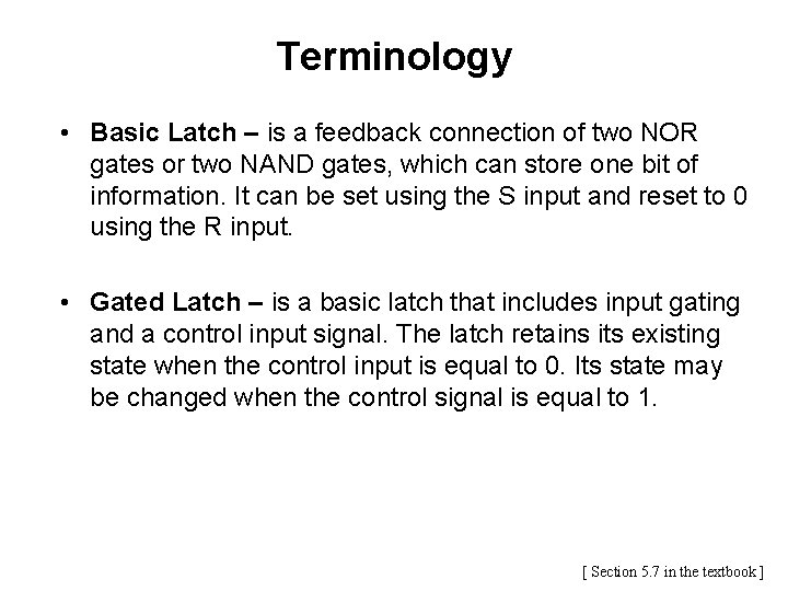
Terminology • Basic Latch – is a feedback connection of two NOR gates or two NAND gates, which can store one bit of information. It can be set using the S input and reset to 0 using the R input. • Gated Latch – is a basic latch that includes input gating and a control input signal. The latch retains its existing state when the control input is equal to 0. Its state may be changed when the control signal is equal to 1. [ Section 5. 7 in the textbook ]

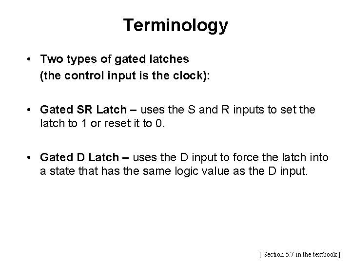
Terminology • Two types of gated latches (the control input is the clock): • Gated SR Latch – uses the S and R inputs to set the latch to 1 or reset it to 0. • Gated D Latch – uses the D input to force the latch into a state that has the same logic value as the D input. [ Section 5. 7 in the textbook ]

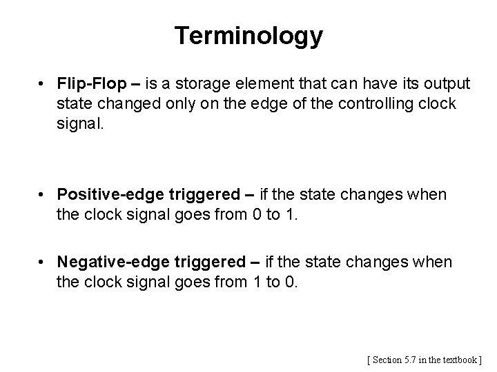
Terminology • Flip-Flop – is a storage element that can have its output state changed only on the edge of the controlling clock signal. • Positive-edge triggered – if the state changes when the clock signal goes from 0 to 1. • Negative-edge triggered – if the state changes when the clock signal goes from 1 to 0. [ Section 5. 7 in the textbook ]

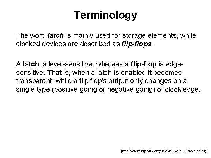
Terminology The word latch is mainly used for storage elements, while clocked devices are described as flip-flops. A latch is level-sensitive, whereas a flip-flop is edgesensitive. That is, when a latch is enabled it becomes transparent, while a flip flop's output only changes on a single type (positive going or negative going) of clock edge. [http: //en. wikipedia. org/wiki/Flip-flop_(electronics)]

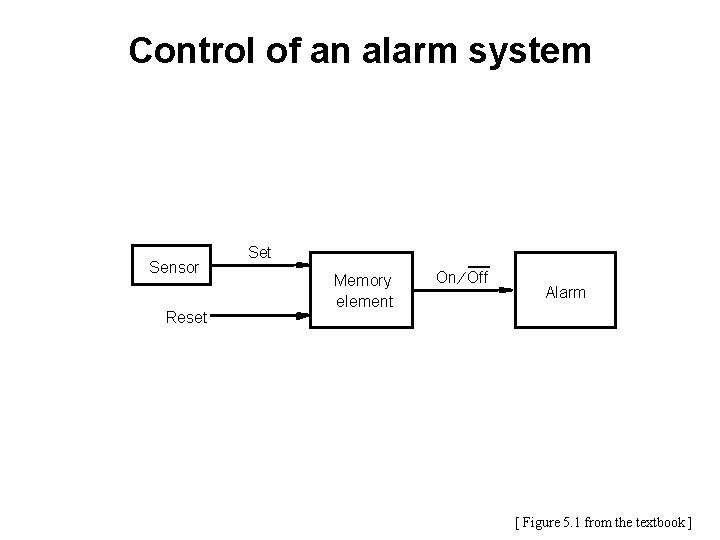
Control of an alarm system Sensor Reset Set Memory element On ¤ Off Alarm [ Figure 5. 1 from the textbook ]

Motivation So far, our circuits have just been converting inputs to outputs. To do more advanced things (i. e. to make computers) we need components that can store data. Can we make a component that “remembers” from the components that we know?
![A simple memory element A B Figure 5 2 from the textbook A simple memory element A B [ Figure 5. 2 from the textbook ]](https://slidetodoc.com/presentation_image_h2/7398568bfce903c5f4ff709b4e0a69cc/image-14.jpg)
A simple memory element A B [ Figure 5. 2 from the textbook ]

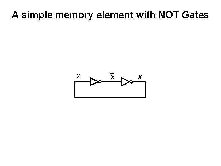
A simple memory element with NOT Gates x x x
![A Strange Loop http animalsiadmire blogspot com201107stupidsnakeeatingitself html A Strange Loop [http: //animalsiadmire. blogspot. com/2011/07/stupid-snake-eating-itself. html]](https://slidetodoc.com/presentation_image_h2/7398568bfce903c5f4ff709b4e0a69cc/image-16.jpg)
A Strange Loop [http: //animalsiadmire. blogspot. com/2011/07/stupid-snake-eating-itself. html]

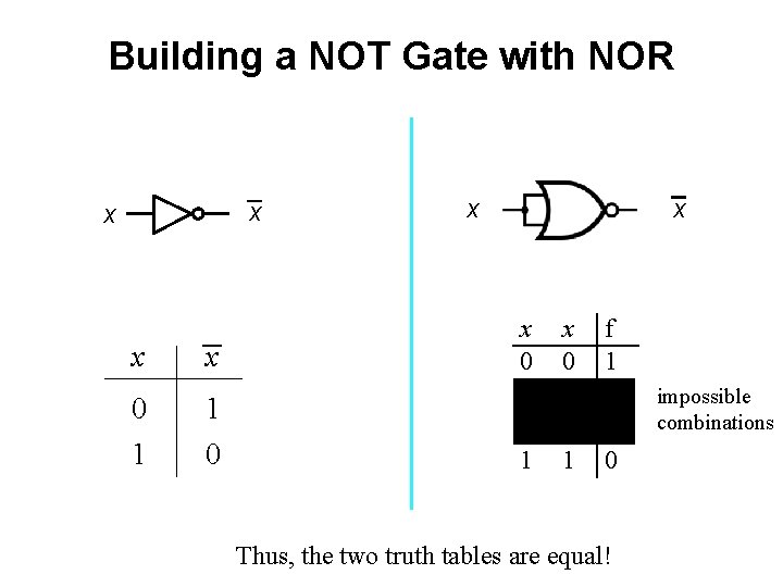
Building a NOT Gate with NAND x x x 0 1 x 1 0 x x x 0 0 1 1 x 0 1 f 1 1 1 0 Thus, the two truth tables are equal! impossible combinations

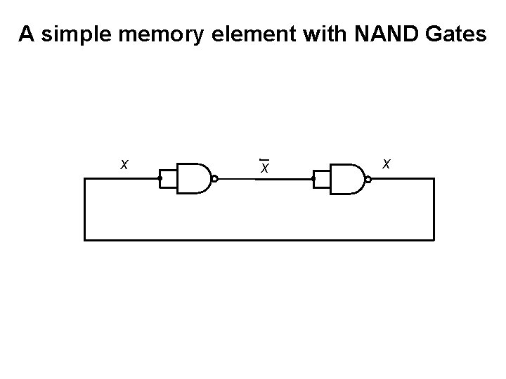
A simple memory element with NAND Gates x x x

Building a NOT Gate with NOR x x x 0 1 x 1 0 x x x 0 0 1 1 x 0 1 f 1 0 0 0 Thus, the two truth tables are equal! impossible combinations

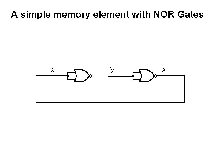
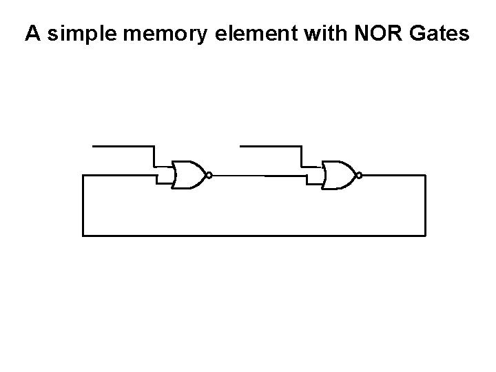
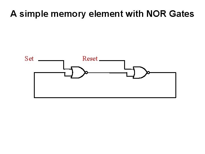
A simple memory element with NOR Gates x x x

Basic Latch

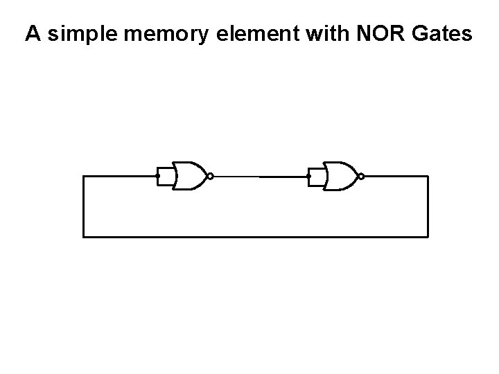
A simple memory element with NOR Gates

A simple memory element with NOR Gates

A simple memory element with NOR Gates Set Reset

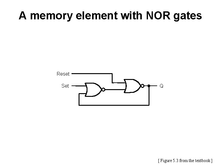
A memory element with NOR gates Reset Set Q [ Figure 5. 3 from the textbook ]

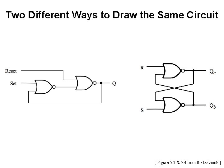
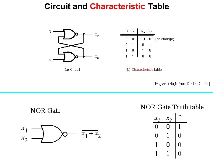
Two Different Ways to Draw the Same Circuit [ Figure 5. 3 & 5. 4 from the textbook ]

Before We Analyze the Basic Latch Let's Look at a Two Simpler Examples with Feedback

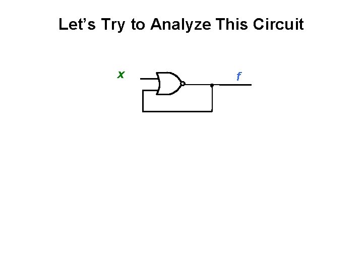
Let’s Try to Analyze This Circuit x f

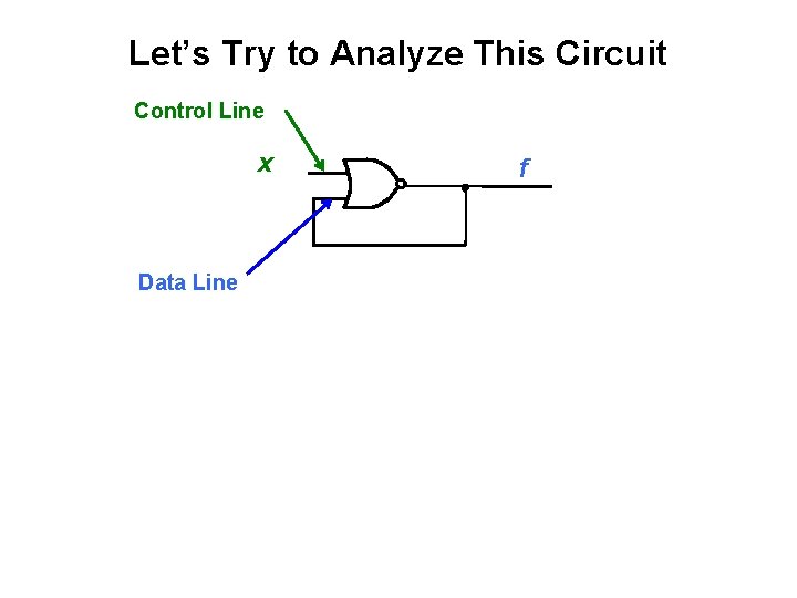
Let’s Try to Analyze This Circuit Control Line x Data Line f

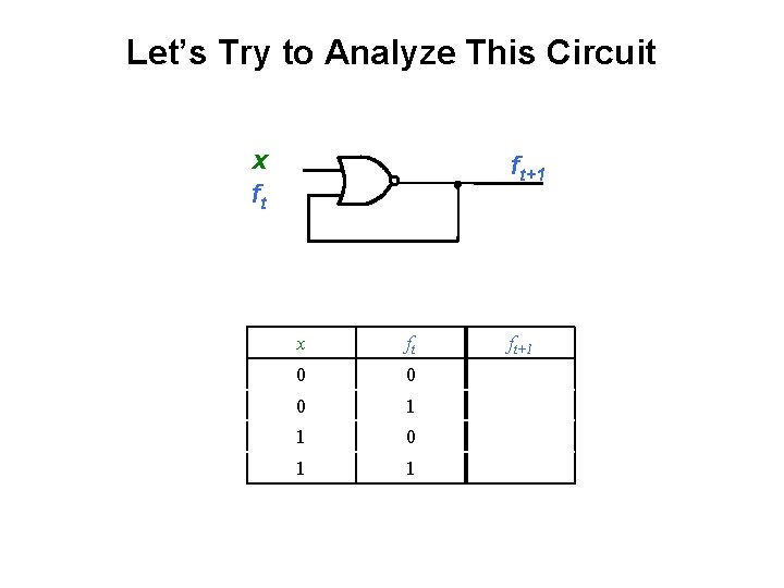
Let’s Try to Analyze This Circuit x ft ft+1 x ft 0 0 0 1 1 ft+1

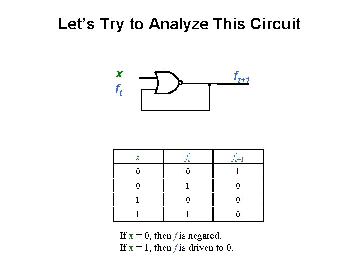
Let’s Try to Analyze This Circuit x ft ft+1 0 0 1 0 1 0 0 1 1 0 If x = 0, then f is negated. If x = 1, then f is driven to 0.

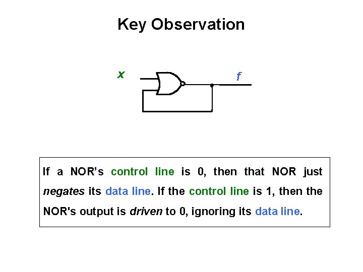
Key Observation x f If a NOR’s control line is 0, then that NOR just negates its data line. If the control line is 1, then the NOR's output is driven to 0, ignoring its data line.

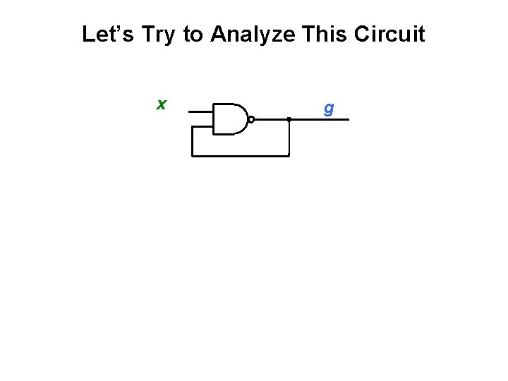
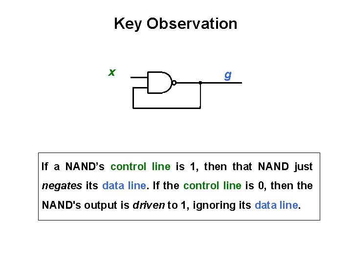
Let’s Try to Analyze This Circuit x g

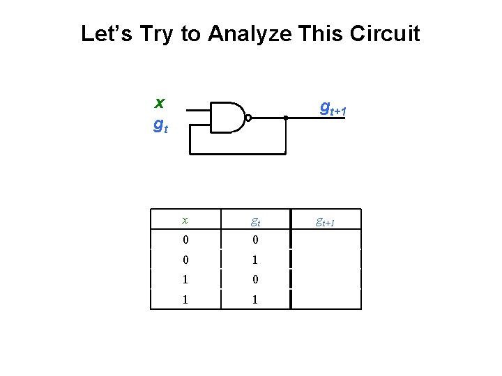
Let’s Try to Analyze This Circuit x gt gt+1 x gt 0 0 0 1 1 gt+1

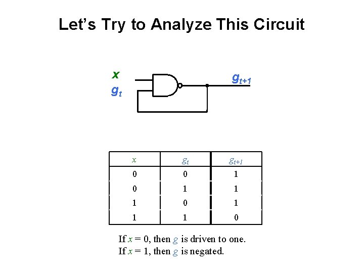
Let’s Try to Analyze This Circuit x gt gt+1 0 0 1 1 1 0 If x = 0, then g is driven to one. If x = 1, then g is negated.

Key Observation x g If a NAND’s control line is 1, then that NAND just negates its data line. If the control line is 0, then the NAND's output is driven to 1, ignoring its data line.

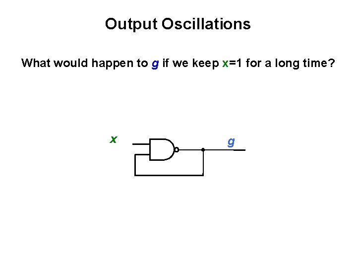
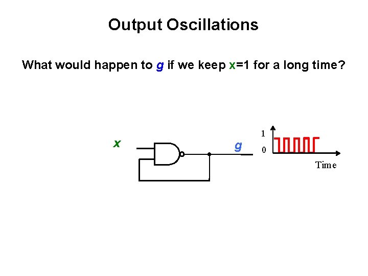
Output Oscillations What would happen to g if we keep x=1 for a long time? x g

Output Oscillations What would happen to g if we keep x=1 for a long time? x g 1 0 Time

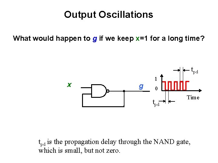
Output Oscillations What would happen to g if we keep x=1 for a long time? tpd x g 1 0 tpd Time tpd is the propagation delay through the NAND gate, which is small, but not zero.

Back to the Basic Latch
![The Basic Latch Q Figure 5 3 from the textbook The Basic Latch Q [ Figure 5. 3 from the textbook ]](https://slidetodoc.com/presentation_image_h2/7398568bfce903c5f4ff709b4e0a69cc/image-41.jpg)
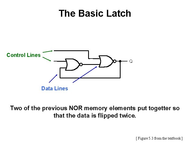
The Basic Latch Q [ Figure 5. 3 from the textbook ]

The Basic Latch Control Lines Q Data Lines Two of the previous NOR memory elements put togetter so that the data is flipped twice. [ Figure 5. 3 from the textbook ]

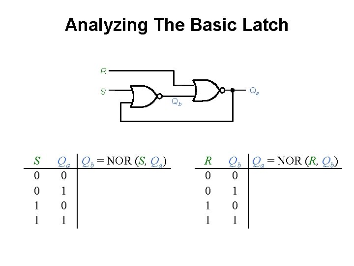
Analyzing The Basic Latch R Qa S Qb S 0 0 1 1 Qa Qb = NOR (S, Qa) 0 1 R 0 0 1 1 Qb Qa = NOR (R, Qb) 0 1

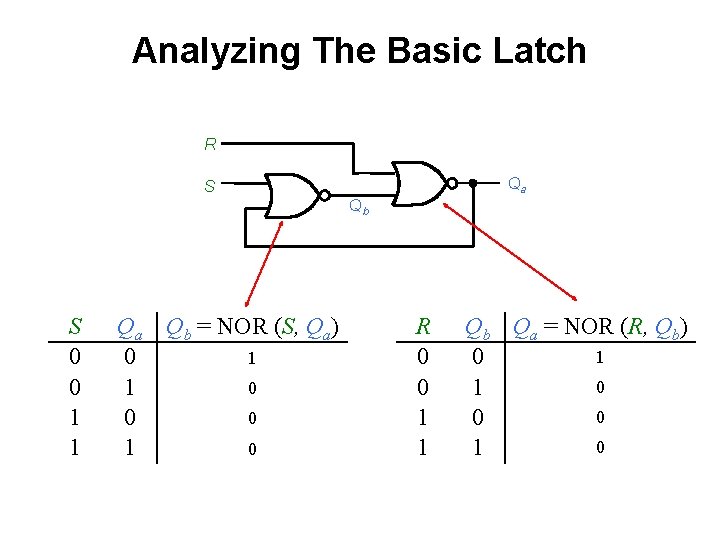
Analyzing The Basic Latch R Qa S Qb S 0 0 1 1 Qa Qb = NOR (S, Qa) 1 0 0 0 1 R 0 0 1 1 Qb Qa = NOR (R, Qb) 1 0 0 0 1

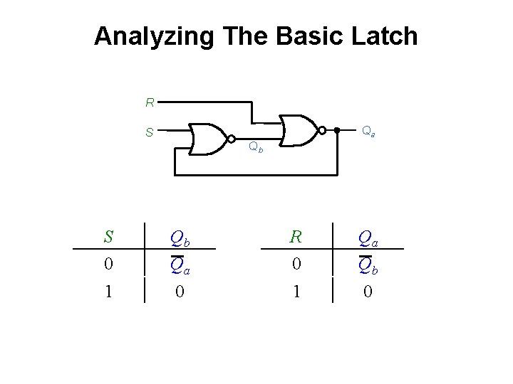
Analyzing The Basic Latch R Qa S Qb S 0 1 Qb Qa 0 R 0 1 Qa Qb 0

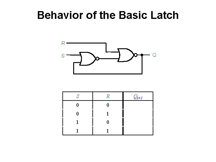
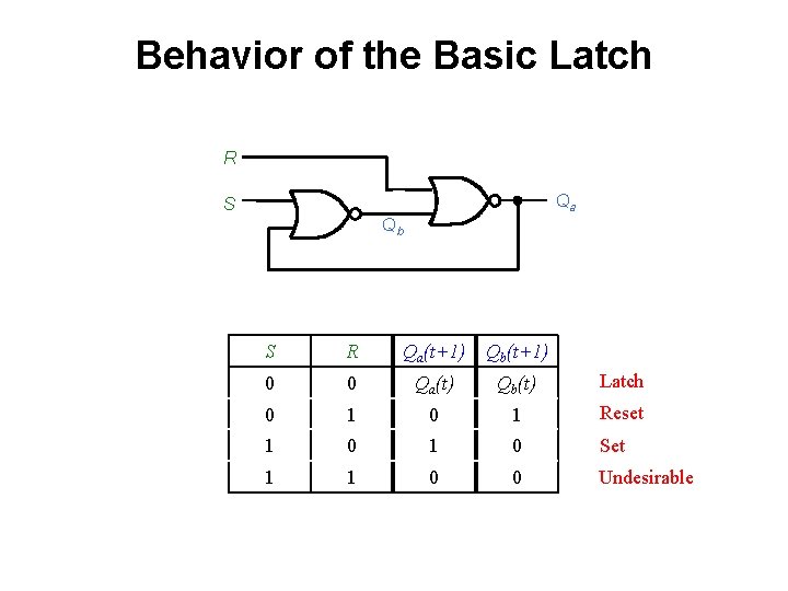
Behavior of the Basic Latch R Q S S R 0 0 0 1 1 Qt+1

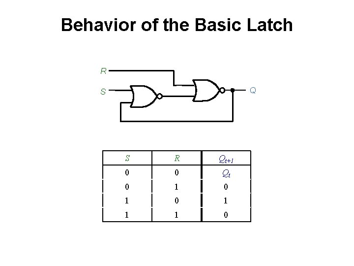
Behavior of the Basic Latch R Q S S R Qt+1 0 0 Qt 0 1 0 1 1 1 0

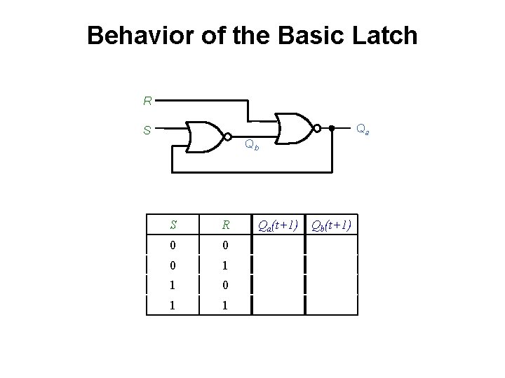
Behavior of the Basic Latch R Qa S Qb S R 0 0 0 1 1 Qa(t+1) Qb(t+1)

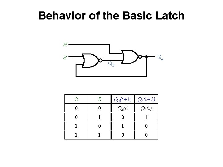
Behavior of the Basic Latch R Qa S Qb S R Qa(t+1) Qb(t+1) 0 0 Qa(t) Qb(t) 0 1 0 1 1 0 0

Behavior of the Basic Latch R Qa S Qb S R Qa(t+1) Qb(t+1) 0 0 Qa(t) Qb(t) Latch 0 1 Reset 1 0 Set 1 1 0 0 Undesirable

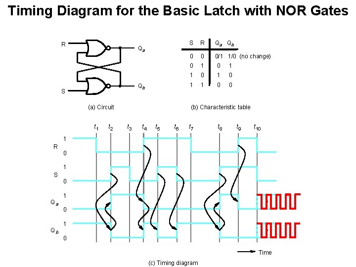
Circuit and Characteristic Table R Qa Qb S (a) Circuit S R Qa Qb 0 0 0/1 1/0 (no change) 0 1 0 1 1 0 0 (b) Characteristic table [ Figure 5. 4 a, b from the textbook ] NOR Gate Truth table x 1 0 0 1 1 x 2 0 1 f 1 0 0 0

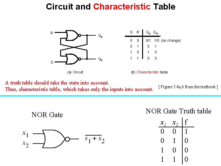
Circuit and Characteristic Table R Qa Qb S (a) Circuit S R Qa Qb 0 0 0/1 1/0 (no change) 0 1 0 1 1 0 0 (b) Characteristic table A truth table should take the state into account. Thus, characteristic table, which takes only the inputs into account. NOR Gate [ Figure 5. 4 a, b from the textbook ] NOR Gate Truth table x 1 0 0 1 1 x 2 0 1 f 1 0 0 0

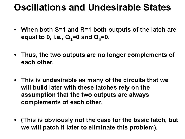
Oscillations and Undesirable States • When both S=1 and R=1 both outputs of the latch are equal to 0, i. e. , Qa=0 and Qb=0. • Thus, the two outputs are no longer complements of each other. • This is undesirable as many of the circuits that we will build later with these latches rely on the assumption that the two outputs are always complements of each other. • (This is obviously not the case for the basic latch, but we will patch it later to eliminate this problem).

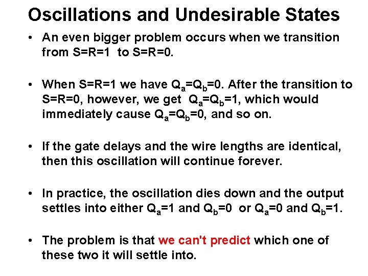
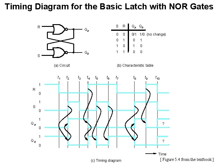
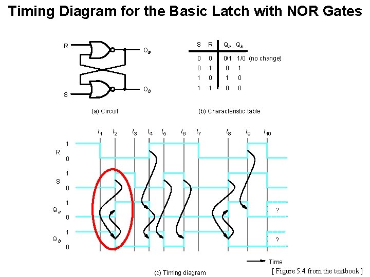
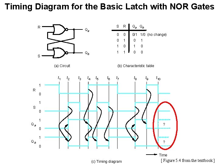
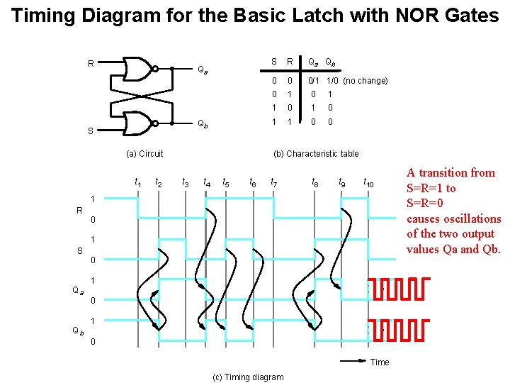
Oscillations and Undesirable States • An even bigger problem occurs when we transition from S=R=1 to S=R=0. • When S=R=1 we have Qa=Qb=0. After the transition to S=R=0, however, we get Qa=Qb=1, which would immediately cause Qa=Qb=0, and so on. • If the gate delays and the wire lengths are identical, then this oscillation will continue forever. • In practice, the oscillation dies down and the output settles into either Qa=1 and Qb=0 or Qa=0 and Qb=1. • The problem is that we can't predict which one of these two it will settle into.

Timing Diagram for the Basic Latch with NOR Gates R Qa Qb S (a) Circuit t 1 t 2 S R Qa Qb 0 0 0/1 1/0 (no change) 0 1 0 1 1 0 0 (b) Characteristic table t 3 t 4 t 5 t 6 t 7 t 8 t 9 t 10 1 R 0 1 S Qa Qb 0 1 ? 0 Time (c) Timing diagram [ Figure 5. 4 from the textbook ]

Timing Diagram for the Basic Latch with NOR Gates R Qa Qb S (a) Circuit t 1 t 2 S R Qa Qb 0 0 0/1 1/0 (no change) 0 1 0 1 1 0 0 (b) Characteristic table t 3 t 4 t 5 t 6 t 7 t 8 t 9 t 10 1 R 0 1 S Qa Qb 0 1 ? 0 Time (c) Timing diagram [ Figure 5. 4 from the textbook ]

Timing Diagram for the Basic Latch with NOR Gates R Qa Qb S (a) Circuit t 1 t 2 S R Qa Qb 0 0 0/1 1/0 (no change) 0 1 0 1 1 0 0 (b) Characteristic table t 3 t 4 t 5 t 6 t 7 t 8 t 9 t 10 1 R 0 1 S Qa Qb 0 1 ? 0 Time (c) Timing diagram [ Figure 5. 4 from the textbook ]

Timing Diagram for the Basic Latch with NOR Gates R Qa Qb S (a) Circuit t 1 t 2 S R Qa Qb 0 0 0/1 1/0 (no change) 0 1 0 1 1 0 0 (b) Characteristic table t 3 t 4 t 5 t 6 t 7 t 8 t 9 t 10 1 R 0 1 S Qa Qb 0 1 ? 0 Time (c) Timing diagram

Timing Diagram for the Basic Latch with NOR Gates R Qa Qb S (a) Circuit t 1 t 2 S R Qa Qb 0 0 0/1 1/0 (no change) 0 1 0 1 1 0 0 (b) Characteristic table t 3 t 4 t 5 t 6 t 7 t 8 t 9 A transition from S=R=1 to S=R=0 causes oscillations of the two output values Qa and Qb. t 10 1 R 0 1 S Qa Qb 0 1 ? 0 Time (c) Timing diagram

Basic Latch with NAND Gates

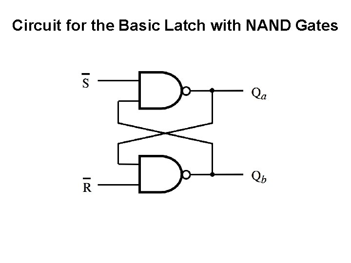
Circuit for the Basic Latch with NAND Gates

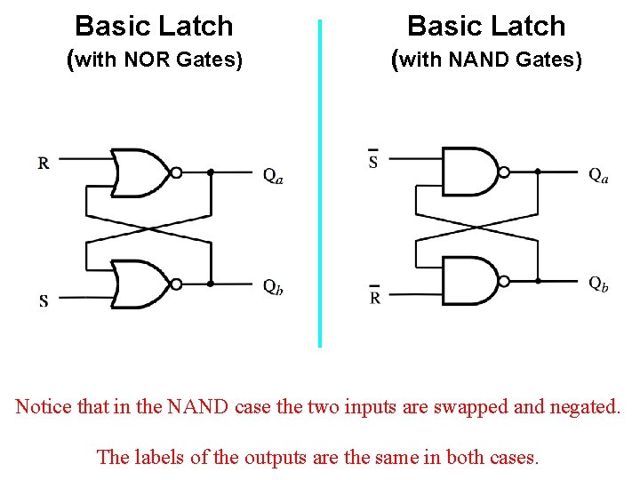
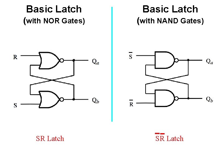
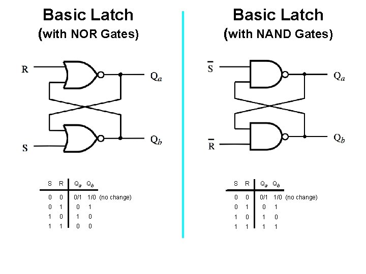
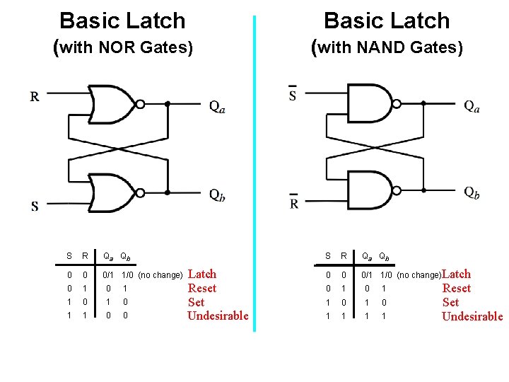
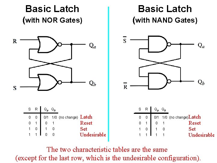
Basic Latch (with NOR Gates) (with NAND Gates) Notice that in the NAND case the two inputs are swapped and negated. The labels of the outputs are the same in both cases.

Basic Latch (with NOR Gates) (with NAND Gates) SR Latch

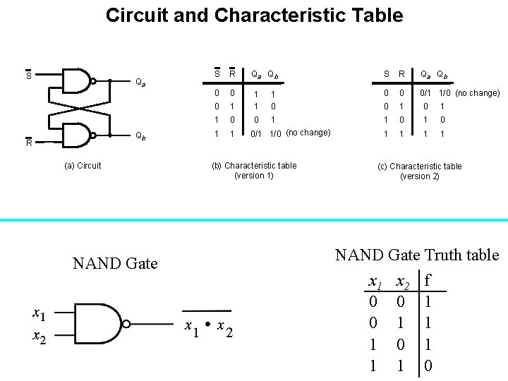
Circuit and Characteristic Table S Qa Qb R (a) Circuit NAND Gate S R 0 0 0 Qa Qb S R Qa Qb 0/1 1/0 (no change) 1 0 0 0 1 1 1 0 0 1 1 1 0/1 1/0 (no change) (b) Characteristic table (version 1) (c) Characteristic table (version 2) NAND Gate Truth table x 1 0 0 1 1 x 2 0 1 f 1 1 1 0

Basic Latch (with NOR Gates) (with NAND Gates) S R Qa Qb 0 0 0/1 1/0 (no change) 0 1 0 1 1 0 0 1 1

Basic Latch (with NOR Gates) (with NAND Gates) S R Qa Qb 0 0 0/1 1/0 (no change) 0 1 0 1 1 0 0 Latch Reset Set Undesirable S R Qa Qb 0 0 0/1 1/0 (no change)Latch 0 1 0 1 1 1 1 Reset Set Undesirable

Basic Latch (with NOR Gates) (with NAND Gates) S R Qa Qb 0 0 0/1 1/0 (no change) 0 1 0 1 1 0 0 Latch Reset Set Undesirable S R Qa Qb 0 0 0/1 1/0 (no change)Latch 0 1 0 1 1 1 1 Reset Set Undesirable The two characteristic tables are the same (except for the last row, which is the undesirable configuration).

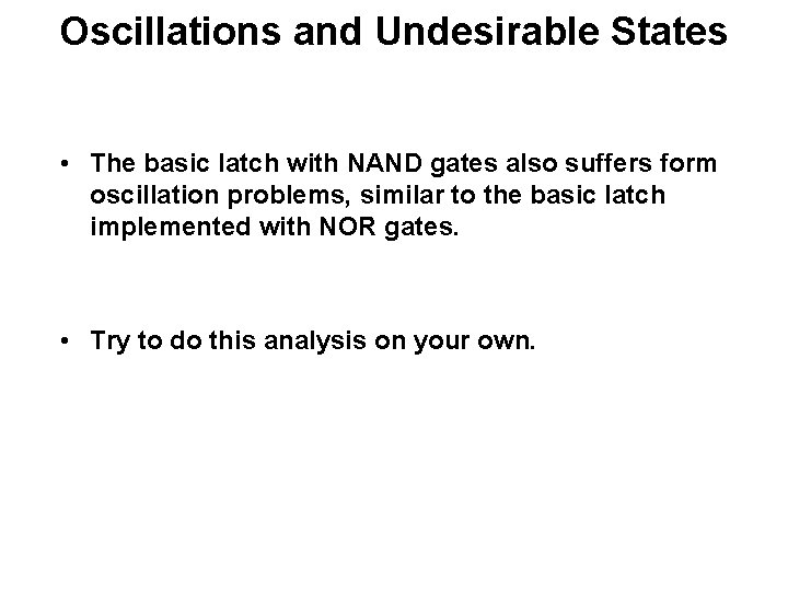
Oscillations and Undesirable States • The basic latch with NAND gates also suffers form oscillation problems, similar to the basic latch implemented with NOR gates. • Try to do this analysis on your own.

Gated SR Latch

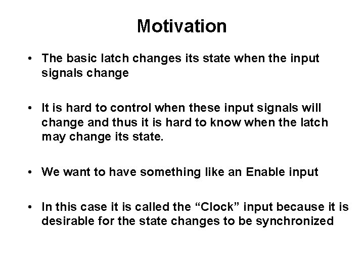
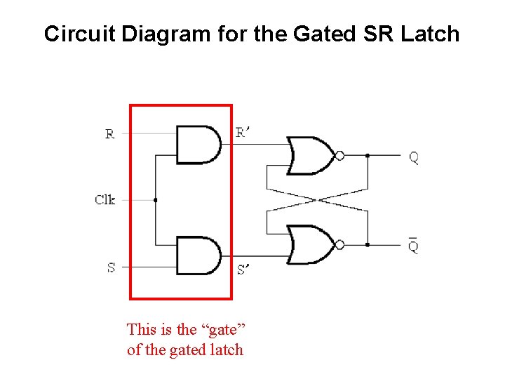
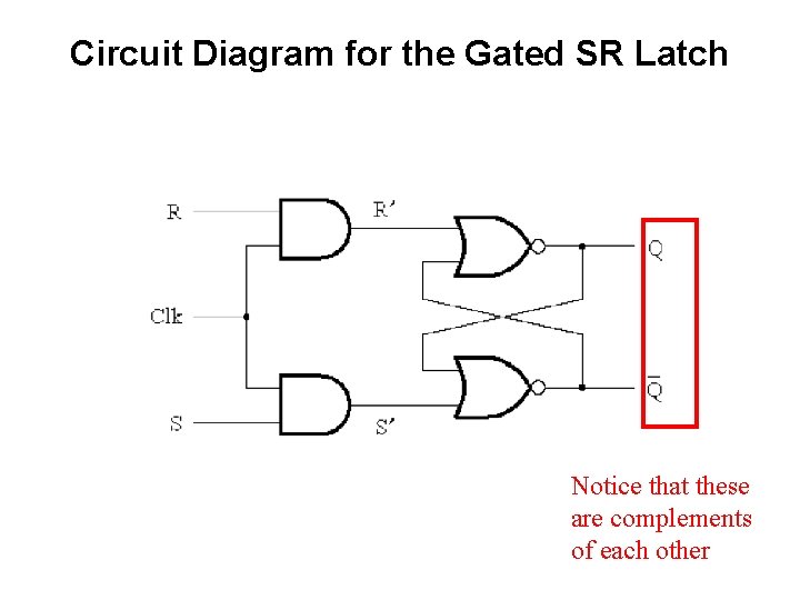
Motivation • The basic latch changes its state when the input signals change • It is hard to control when these input signals will change and thus it is hard to know when the latch may change its state. • We want to have something like an Enable input • In this case it is called the “Clock” input because it is desirable for the state changes to be synchronized

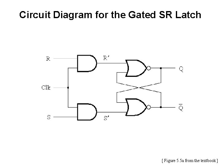
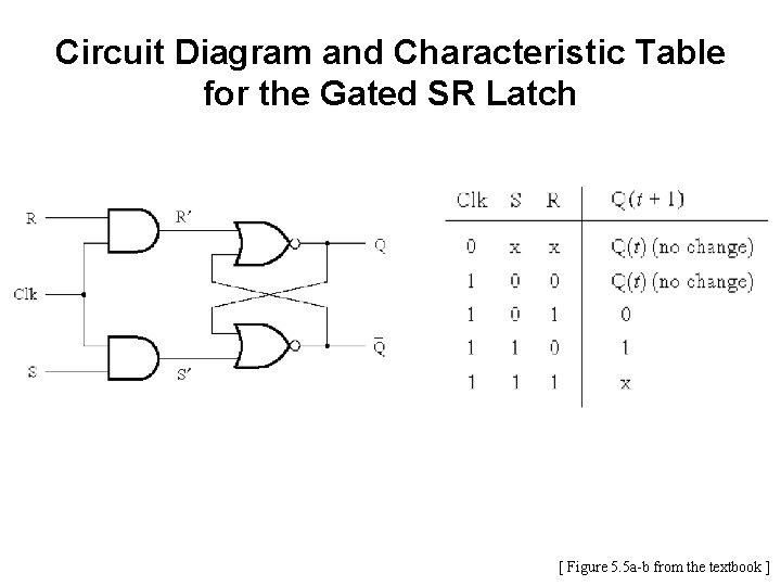
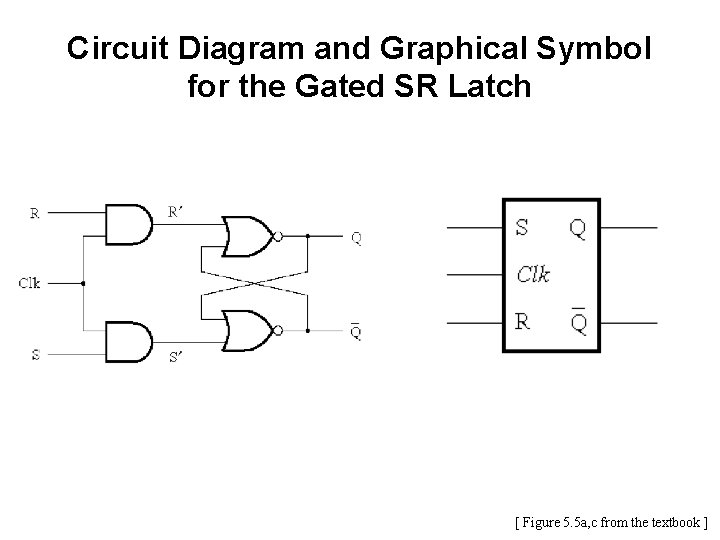
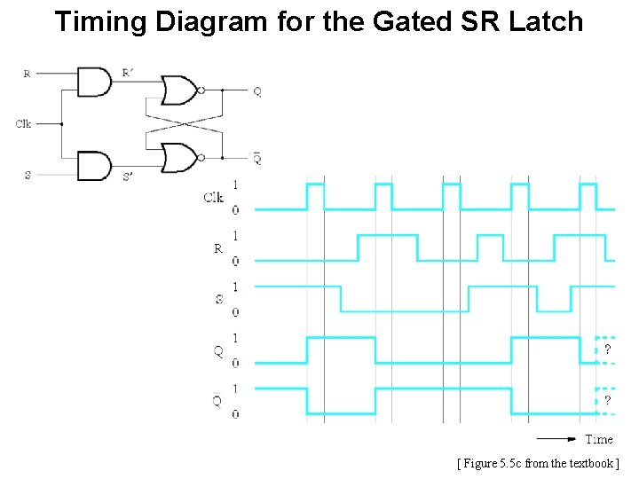
Circuit Diagram for the Gated SR Latch [ Figure 5. 5 a from the textbook ]

Circuit Diagram for the Gated SR Latch This is the “gate” of the gated latch

Circuit Diagram for the Gated SR Latch Notice that these are complements of each other

Circuit Diagram and Characteristic Table for the Gated SR Latch [ Figure 5. 5 a-b from the textbook ]

Circuit Diagram and Graphical Symbol for the Gated SR Latch [ Figure 5. 5 a, c from the textbook ]

Timing Diagram for the Gated SR Latch [ Figure 5. 5 c from the textbook ]

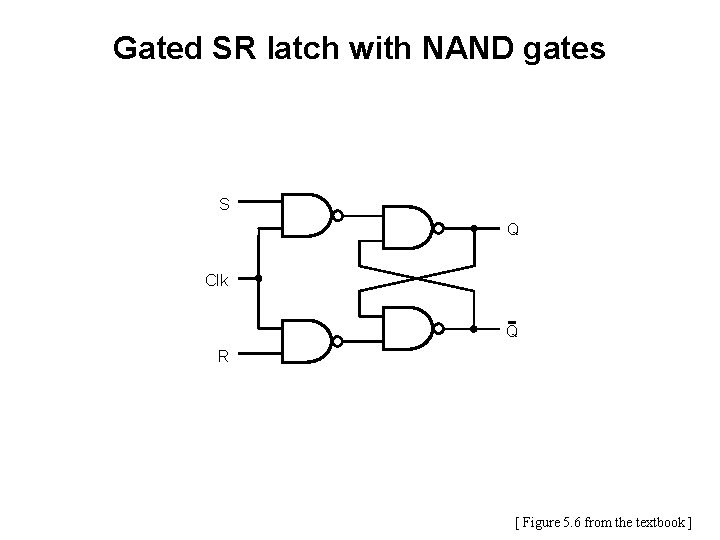
Gated SR latch with NAND gates S Q Clk Q R [ Figure 5. 6 from the textbook ]

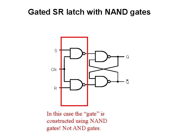
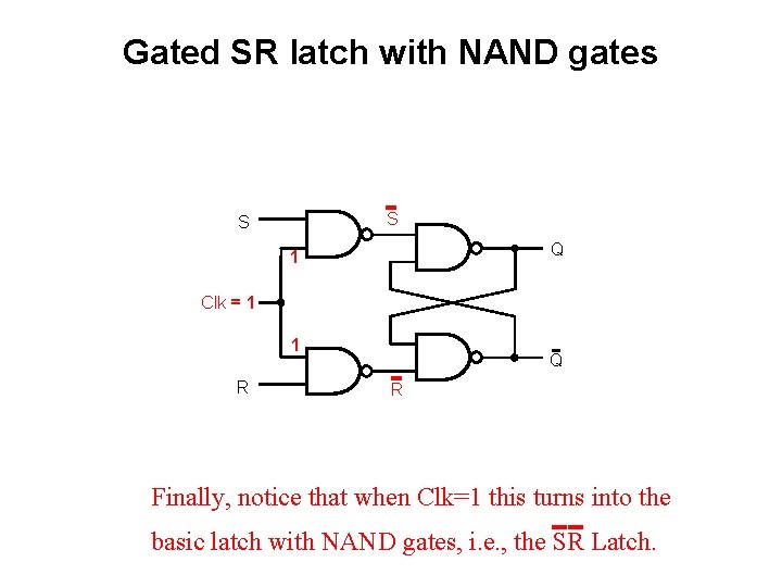
Gated SR latch with NAND gates S Q Clk Q R In this case the “gate” is constructed using NAND gates! Not AND gates.

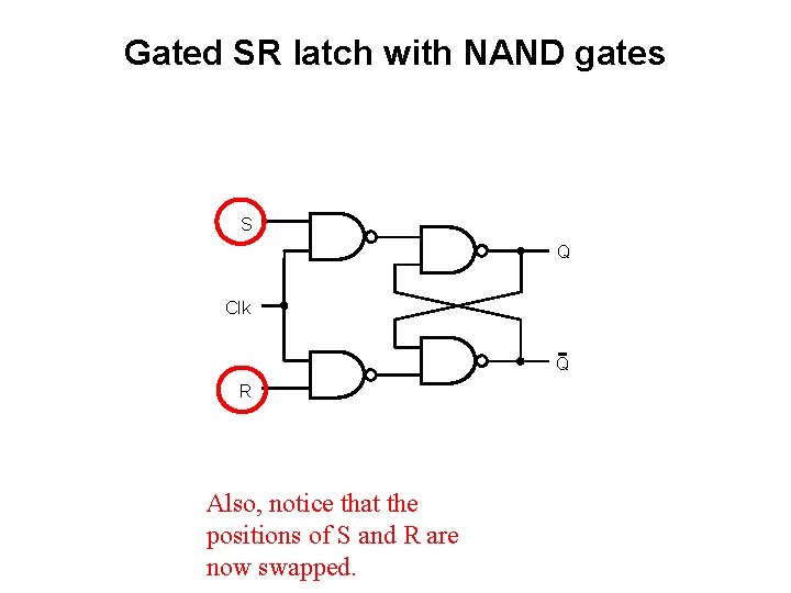
Gated SR latch with NAND gates S Q Clk Q R Also, notice that the positions of S and R are now swapped.

Gated SR latch with NAND gates S S Q 1 Clk = 1 1 R Q R Finally, notice that when Clk=1 this turns into the basic latch with NAND gates, i. e. , the SR Latch.

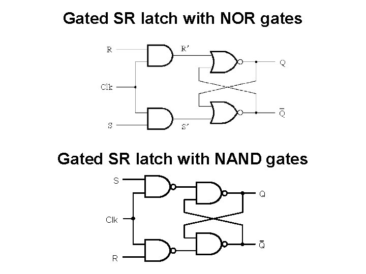
Gated SR latch with NOR gates Gated SR latch with NAND gates S Q Clk Q R

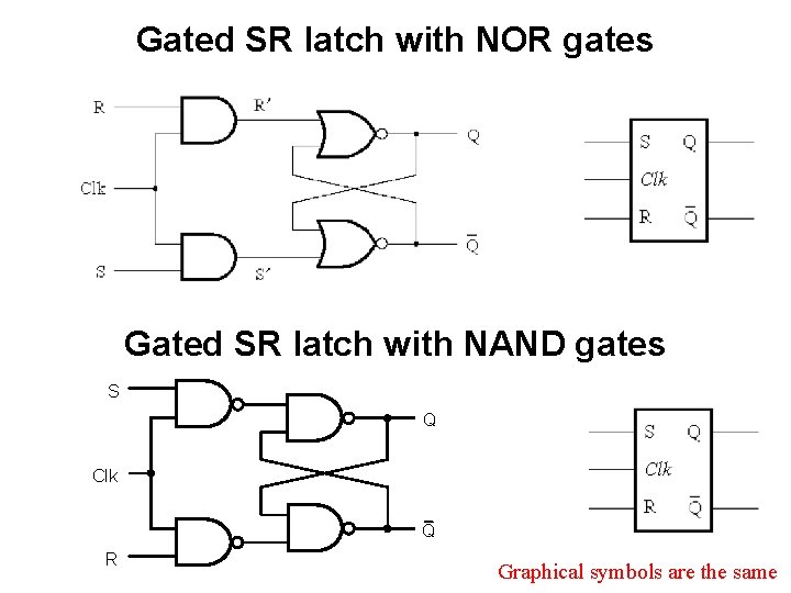
Gated SR latch with NOR gates Gated SR latch with NAND gates S Q Clk Q R Graphical symbols are the same

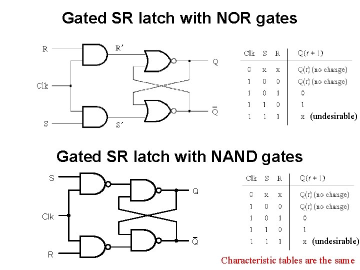
Gated SR latch with NOR gates (undesirable) Gated SR latch with NAND gates S Q Clk Q R (undesirable) Characteristic tables are the same

Gated D Latch

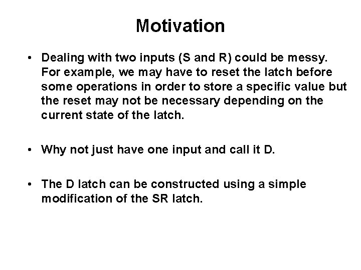
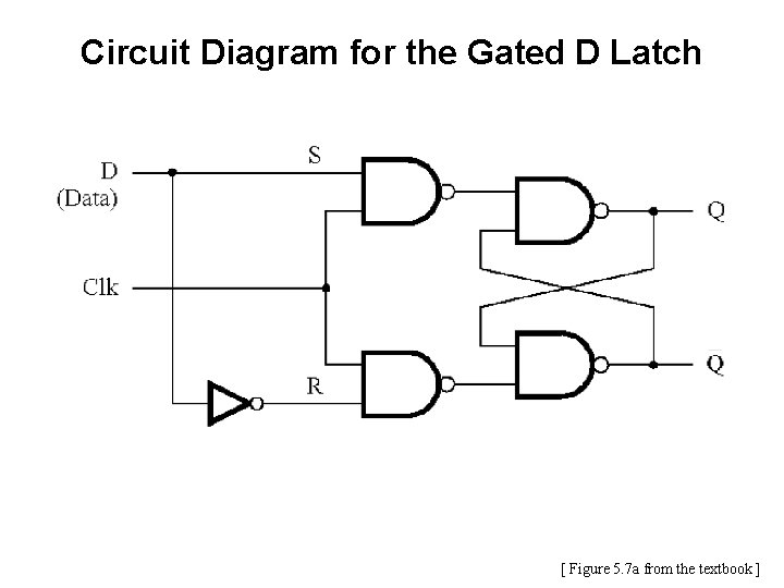
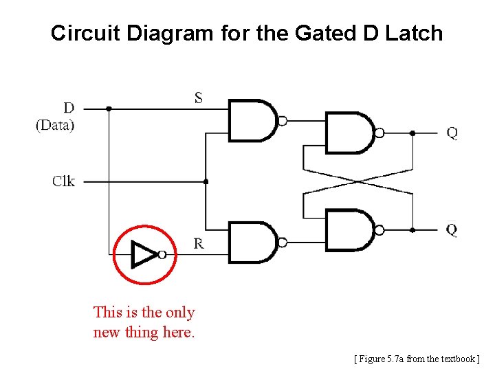
Motivation • Dealing with two inputs (S and R) could be messy. For example, we may have to reset the latch before some operations in order to store a specific value but the reset may not be necessary depending on the current state of the latch. • Why not just have one input and call it D. • The D latch can be constructed using a simple modification of the SR latch.

Circuit Diagram for the Gated D Latch [ Figure 5. 7 a from the textbook ]

Circuit Diagram for the Gated D Latch This is the only new thing here. [ Figure 5. 7 a from the textbook ]

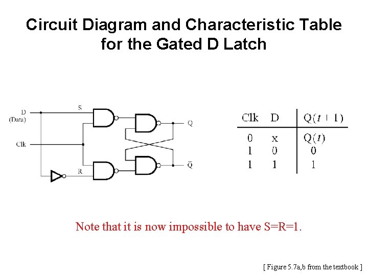
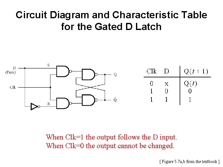
Circuit Diagram and Characteristic Table for the Gated D Latch Note that it is now impossible to have S=R=1. [ Figure 5. 7 a, b from the textbook ]

Circuit Diagram and Characteristic Table for the Gated D Latch When Clk=1 the output follows the D input. When Clk=0 the output cannot be changed. [ Figure 5. 7 a, b from the textbook ]

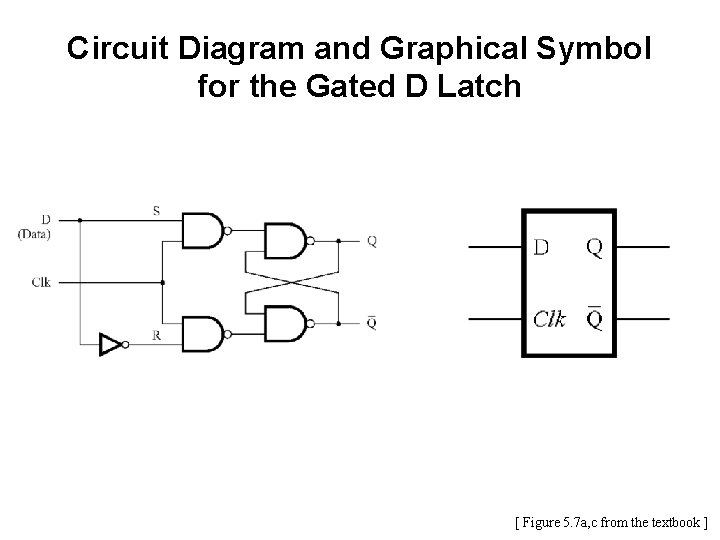
Circuit Diagram and Graphical Symbol for the Gated D Latch [ Figure 5. 7 a, c from the textbook ]

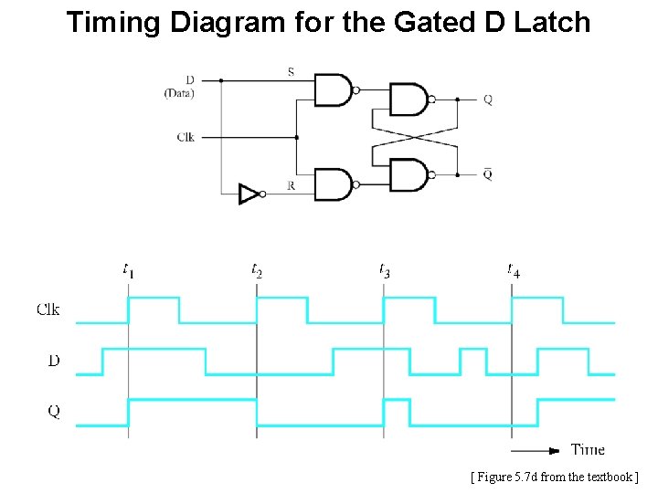
Timing Diagram for the Gated D Latch [ Figure 5. 7 d from the textbook ]

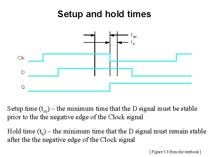
Setup and hold times t su th Clk D Q Setup time (tsu) – the minimum time that the D signal must be stable prior to the negative edge of the Clock signal Hold time (th) – the minimum time that the D signal must remain stable after the negative edge of the Clock signal [ Figure 5. 8 from the textbook ]

Some Practical Examples

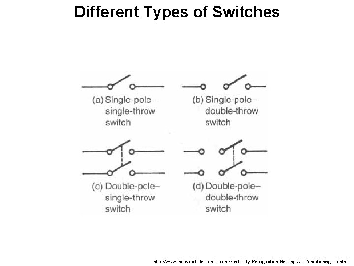
Different Types of Switches http: //www. industrial-electronics. com/Electricity-Refrigeration-Heating-Air-Conditioning_5 b. html

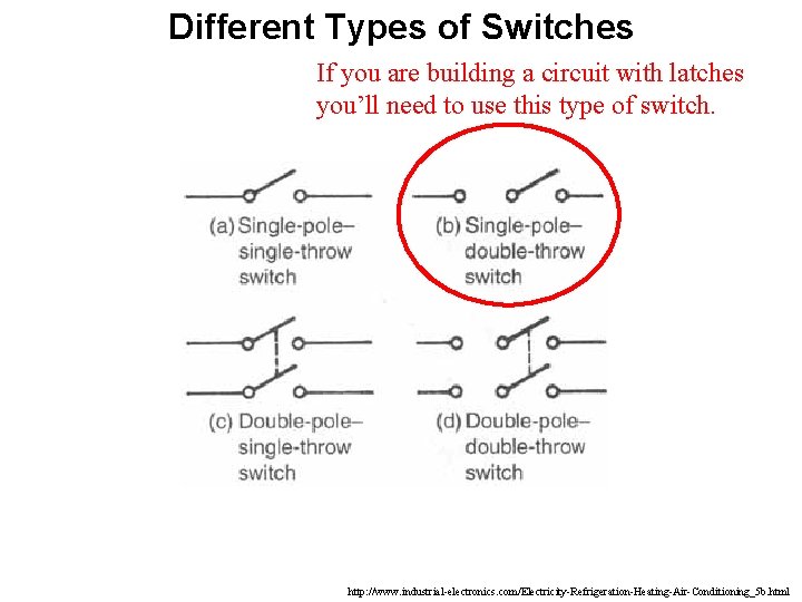
Different Types of Switches If you are building a circuit with latches you’ll need to use this type of switch. http: //www. industrial-electronics. com/Electricity-Refrigeration-Heating-Air-Conditioning_5 b. html
![Single Pole Double Throw SPDT http electronicsclub infoimagesswabc gif Single Pole, Double Throw = SPDT [http: //electronicsclub. info/images/swabc. gif]](https://slidetodoc.com/presentation_image_h2/7398568bfce903c5f4ff709b4e0a69cc/image-96.jpg)
Single Pole, Double Throw = SPDT [http: //electronicsclub. info/images/swabc. gif]
![Single Pole Double Throw SPDT http www cubisteffects comimagesMIYPt 3Throw jpg Single Pole, Double Throw = SPDT [http: //www. cubisteffects. com/images/MIY/Pt 3_Throw. jpg]](https://slidetodoc.com/presentation_image_h2/7398568bfce903c5f4ff709b4e0a69cc/image-97.jpg)
Single Pole, Double Throw = SPDT [http: //www. cubisteffects. com/images/MIY/Pt 3_Throw. jpg]

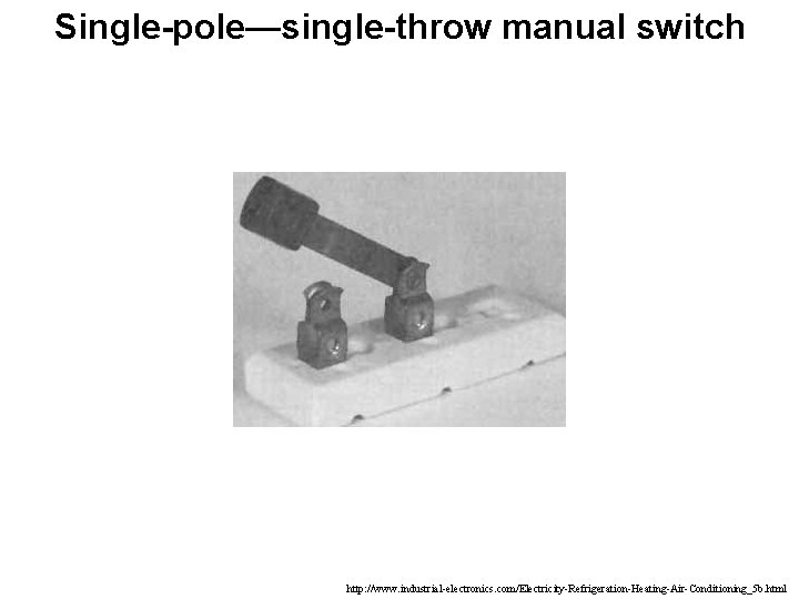
Single-pole—single-throw manual switch http: //www. industrial-electronics. com/Electricity-Refrigeration-Heating-Air-Conditioning_5 b. html

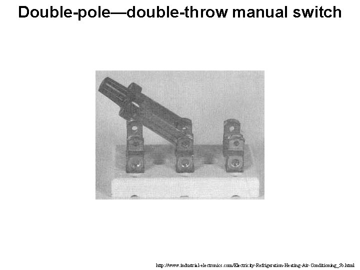
Double-pole—double-throw manual switch http: //www. industrial-electronics. com/Electricity-Refrigeration-Heating-Air-Conditioning_5 b. html

The following examples came from this book
![A Simple Circuit Platt 2009 A Simple Circuit [ Platt 2009 ]](https://slidetodoc.com/presentation_image_h2/7398568bfce903c5f4ff709b4e0a69cc/image-101.jpg)
A Simple Circuit [ Platt 2009 ]
![Lets Take a Closer Look at This Platt 2009 Let’s Take a Closer Look at This [ Platt 2009 ]](https://slidetodoc.com/presentation_image_h2/7398568bfce903c5f4ff709b4e0a69cc/image-102.jpg)
Let’s Take a Closer Look at This [ Platt 2009 ]
![A Similar Example with NAND Gates Platt 2009 A Similar Example with NAND Gates [ Platt 2009 ]](https://slidetodoc.com/presentation_image_h2/7398568bfce903c5f4ff709b4e0a69cc/image-103.jpg)
A Similar Example with NAND Gates [ Platt 2009 ]

Questions?

THE END