
CPEEE 422522 Advanced Logic Design L 03 Electrical
- Slides: 36
CPE/EE 422/522 Advanced Logic Design L 03 Electrical and Computer Engineering University of Alabama in Huntsville UAH-CPE/EE 422/522 AM
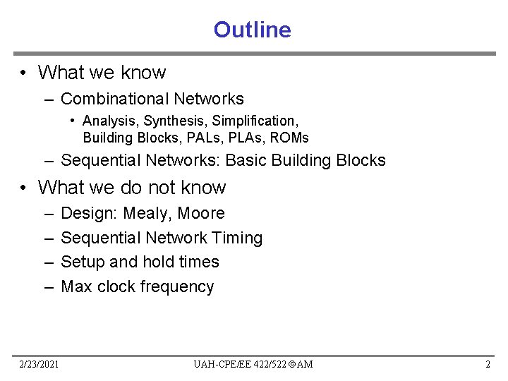
Outline • What we know – Combinational Networks • Analysis, Synthesis, Simplification, Building Blocks, PALs, PLAs, ROMs – Sequential Networks: Basic Building Blocks • What we do not know – – 2/23/2021 Design: Mealy, Moore Sequential Network Timing Setup and hold times Max clock frequency UAH-CPE/EE 422/522 AM 2
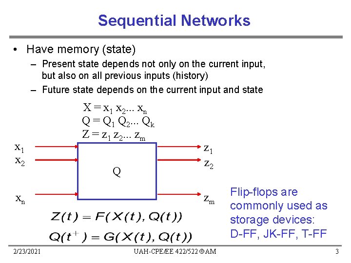
Sequential Networks • Have memory (state) – Present state depends not only on the current input, but also on all previous inputs (history) – Future state depends on the current input and state x 1 x 2 xn 2/23/2021 X = x 1 x 2. . . xn Q = Q 1 Q 2. . . Qk Z = z 1 z 2. . . zm Q z 1 z 2 zm UAH-CPE/EE 422/522 AM Flip-flops are commonly used as storage devices: D-FF, JK-FF, T-FF 3
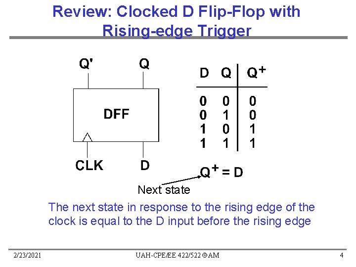
Review: Clocked D Flip-Flop with Rising-edge Trigger Next state The next state in response to the rising edge of the clock is equal to the D input before the rising edge 2/23/2021 UAH-CPE/EE 422/522 AM 4
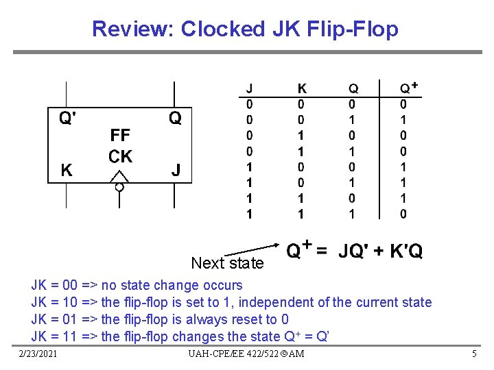
Review: Clocked JK Flip-Flop Next state JK = 00 => no state change occurs JK = 10 => the flip-flop is set to 1, independent of the current state JK = 01 => the flip-flop is always reset to 0 JK = 11 => the flip-flop changes the state Q+ = Q’ 2/23/2021 UAH-CPE/EE 422/522 AM 5
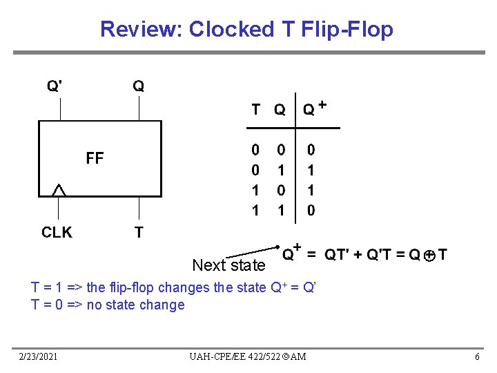
Review: Clocked T Flip-Flop Next state T = 1 => the flip-flop changes the state Q+ = Q’ T = 0 => no state change 2/23/2021 UAH-CPE/EE 422/522 AM 6
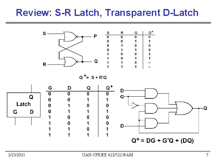
Review: S-R Latch, Transparent D-Latch 2/23/2021 UAH-CPE/EE 422/522 AM 7
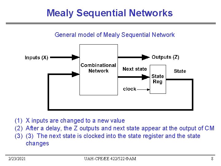
Mealy Sequential Networks General model of Mealy Sequential Network (1) X inputs are changed to a new value (2) After a delay, the Z outputs and next state appear at the output of CM (3) The next state is clocked into the state register and the state changes 2/23/2021 UAH-CPE/EE 422/522 AM 8
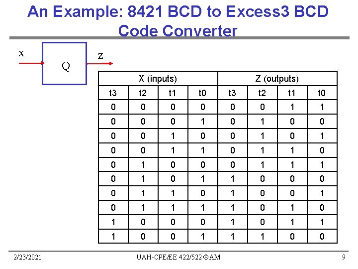
An Example: 8421 BCD to Excess 3 BCD Code Converter x Q z X (inputs) 2/23/2021 Z (outputs) t 3 t 2 t 1 t 0 0 0 0 1 1 0 0 0 1 0 0 1 1 0 0 0 1 1 1 0 0 1 1 0 0 1 1 1 1 0 1 0 0 0 1 1 1 0 0 UAH-CPE/EE 422/522 AM 9
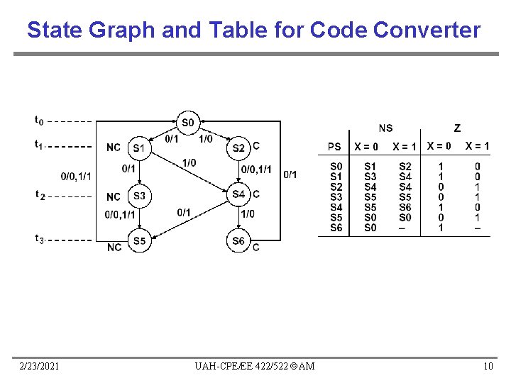
State Graph and Table for Code Converter 2/23/2021 UAH-CPE/EE 422/522 AM 10
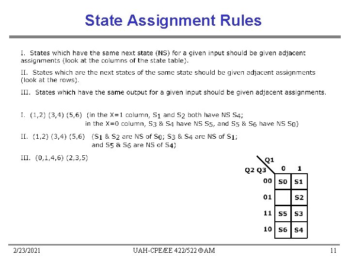
State Assignment Rules 2/23/2021 UAH-CPE/EE 422/522 AM 11
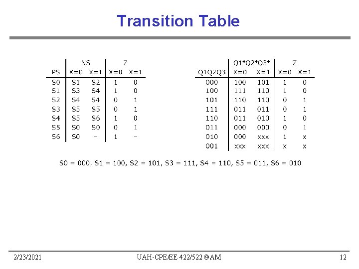
Transition Table 2/23/2021 UAH-CPE/EE 422/522 AM 12
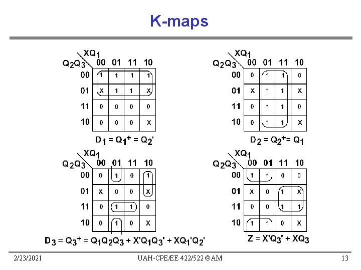
K-maps 2/23/2021 UAH-CPE/EE 422/522 AM 13
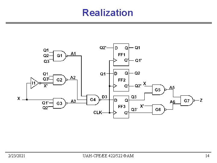
Realization 2/23/2021 UAH-CPE/EE 422/522 AM 14
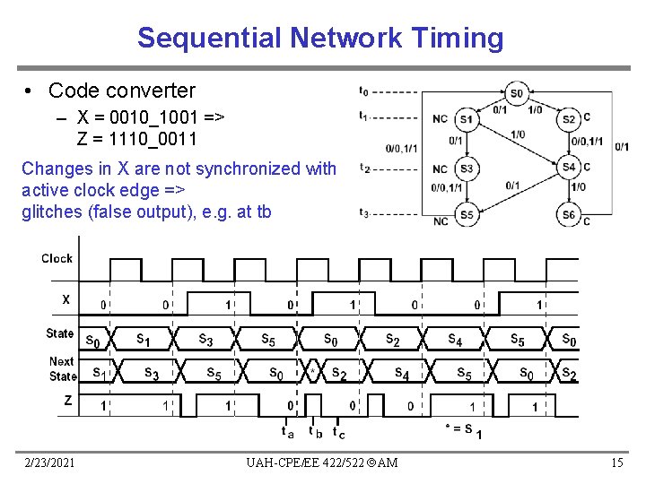
Sequential Network Timing • Code converter – X = 0010_1001 => Z = 1110_0011 Changes in X are not synchronized with active clock edge => glitches (false output), e. g. at tb 2/23/2021 UAH-CPE/EE 422/522 AM 15
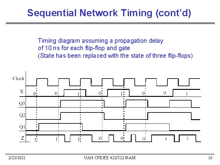
Sequential Network Timing (cont’d) Timing diagram assuming a propagation delay of 10 ns for each flip-flop and gate (State has been replaced with the state of three flip-flops) 2/23/2021 UAH-CPE/EE 422/522 AM 16
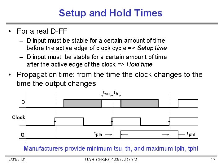
Setup and Hold Times • For a real D-FF – D input must be stable for a certain amount of time before the active edge of clock cycle => Setup time – D input must be stable for a certain amount of time after the active edge of the clock => Hold time • Propagation time: from the time the clock changes to the time the output changes Manufacturers provide minimum tsu, th, and maximum tplh, tphl 2/23/2021 UAH-CPE/EE 422/522 AM 17
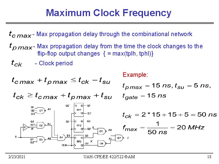
Maximum Clock Frequency - Max propagation delay through the combinational network - Max propagation delay from the time the clock changes to the flip-flop output changes { = max(tplh, tphl)} - Clock period Example: 2/23/2021 UAH-CPE/EE 422/522 AM 18
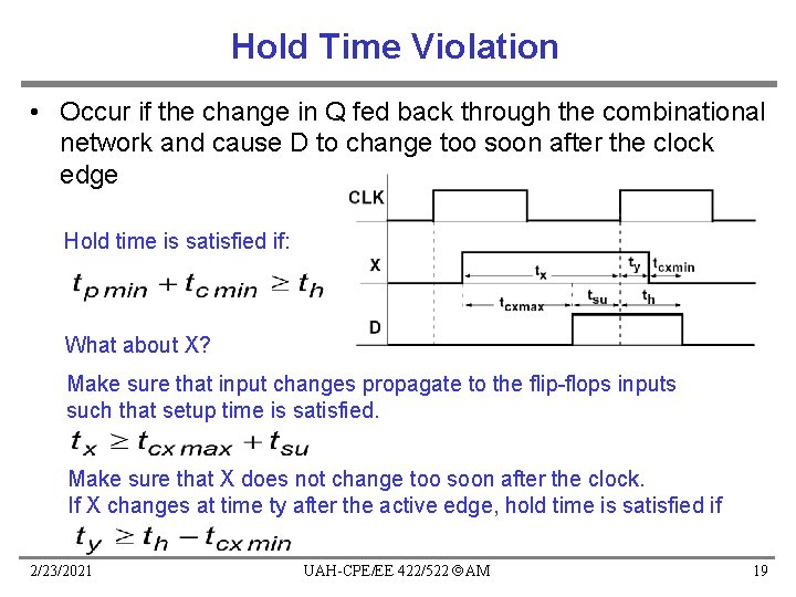
Hold Time Violation • Occur if the change in Q fed back through the combinational network and cause D to change too soon after the clock edge Hold time is satisfied if: What about X? Make sure that input changes propagate to the flip-flops inputs such that setup time is satisfied. Make sure that X does not change too soon after the clock. If X changes at time ty after the active edge, hold time is satisfied if 2/23/2021 UAH-CPE/EE 422/522 AM 19
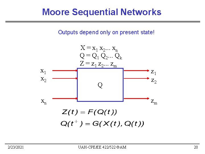
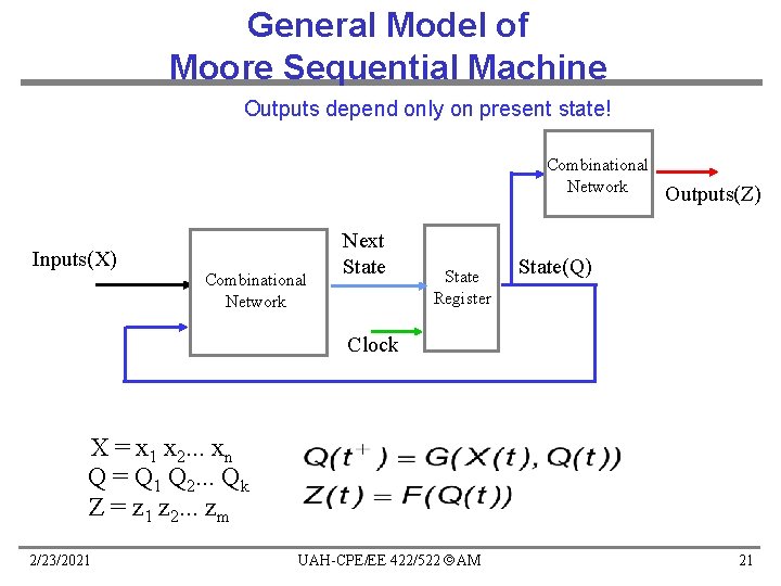
Moore Sequential Networks Outputs depend only on present state! x 1 x 2 X = x 1 x 2. . . xn Q = Q 1 Q 2. . . Qk Z = z 1 z 2. . . zm Q xn 2/23/2021 z 2 zm UAH-CPE/EE 422/522 AM 20
General Model of Moore Sequential Machine Outputs depend only on present state! Combinational Network Inputs(X) Combinational Network Next State Register Outputs(Z) State(Q) Clock X = x 1 x 2. . . xn Q = Q 1 Q 2. . . Qk Z = z 1 z 2. . . zm 2/23/2021 UAH-CPE/EE 422/522 AM 21
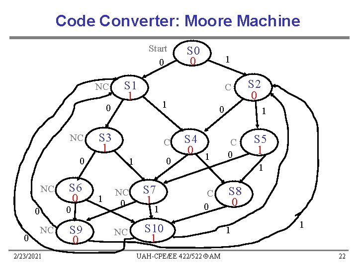
Code Converter: Moore Machine Start 0 NC NC S 1 1 NC 0 0 0 S 6 0 1 S 3 1 C NC 2/23/2021 S 9 0 0 1 1 1 C 0 0 S 0 0 NC 0 S 7 1 NC S 10 1 1 0 S 4 0 1 1 C 0 S 8 0 UAH-CPE/EE 422/522 AM S 2 0 S 5 1 1 22
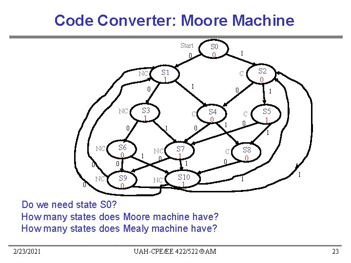
Code Converter: Moore Machine Start 0 NC NC S 1 1 0 0 0 S 6 0 1 S 3 1 C NC S 9 0 0 S 4 0 0 1 1 1 C 0 0 NC S 0 0 NC 0 S 7 1 NC S 10 1 1 1 S 2 0 1 C 0 S 5 1 1 C 0 S 8 0 1 1 Do we need state S 0? How many states does Moore machine have? How many states does Mealy machine have? 2/23/2021 UAH-CPE/EE 422/522 AM 23
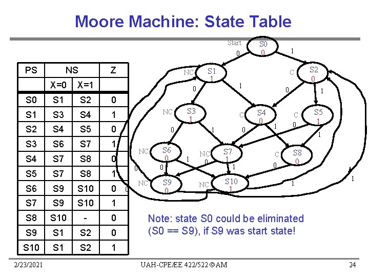
Moore Machine: State Table Start 0 PS NS Z NC X=0 X=1 S 0 S 1 S 2 0 S 1 S 3 S 4 1 NC S 2 S 4 S 5 0 0 S 3 S 6 S 7 1 S 4 S 7 S 8 0 S 5 S 7 S 8 S 9 S 10 0 S 7 S 9 S 10 1 S 8 S 10 - 0 S 9 S 1 S 2 0 S 1 S 2 1 0 S 6 0 0 0 1 S 6 2/23/2021 NC NC S 9 0 S 1 1 S 0 0 C 0 1 S 3 1 C 0 1 1 1 NC 0 S 7 1 NC S 10 1 1 0 S 4 0 1 S 2 0 1 C 0 S 5 1 1 C 0 S 8 0 1 1 Note: state S 0 could be eliminated (S 0 == S 9), if S 9 was start state! UAH-CPE/EE 422/522 AM 24
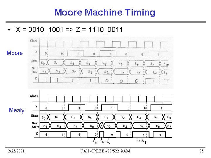
Moore Machine Timing • X = 0010_1001 => Z = 1110_0011 Moore Mealy 2/23/2021 UAH-CPE/EE 422/522 AM 25
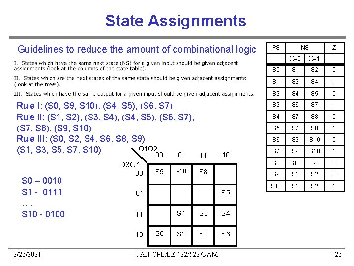
State Assignments Guidelines to reduce the amount of combinational logic Rule I: (S 0, S 9, S 10), (S 4, S 5), (S 6, S 7) Rule II: (S 1, S 2), (S 3, S 4), (S 4, S 5), (S 6, S 7), (S 7, S 8), (S 9, S 10) Rule III: (S 0, S 2, S 4, S 6, S 8, S 9) Q 1 Q 2 (S 1, S 3, S 5, S 7, S 10) 00 Q 3 Q 4 S 0 – 0010 S 1 - 0111 …. S 10 - 0100 00 s 10 11 10 S 8 S 5 01 11 10 2/23/2021 S 9 01 S 0 S 1 S 3 S 4 S 2 S 7 S 6 UAH-CPE/EE 422/522 AM PS NS Z X=0 X=1 S 0 S 1 S 2 0 S 1 S 3 S 4 1 S 2 S 4 S 5 0 S 3 S 6 S 7 1 S 4 S 7 S 8 0 S 5 S 7 S 8 1 S 6 S 9 S 10 0 S 7 S 9 S 10 1 S 8 S 10 - 0 S 9 S 1 S 2 0 S 1 S 2 1 26
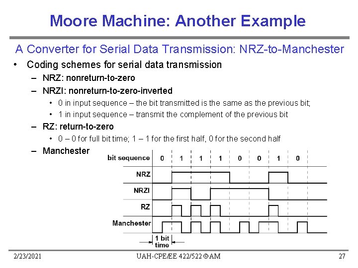
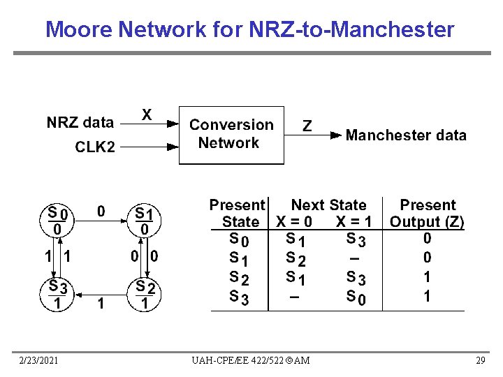
Moore Machine: Another Example A Converter for Serial Data Transmission: NRZ-to-Manchester • Coding schemes for serial data transmission – NRZ: nonreturn-to-zero – NRZI: nonreturn-to-zero-inverted • 0 in input sequence – the bit transmitted is the same as the previous bit; • 1 in input sequence – transmit the complement of the previous bit – RZ: return-to-zero • 0 – 0 for full bit time; 1 – 1 for the first half, 0 for the second half – Manchester 2/23/2021 UAH-CPE/EE 422/522 AM 27
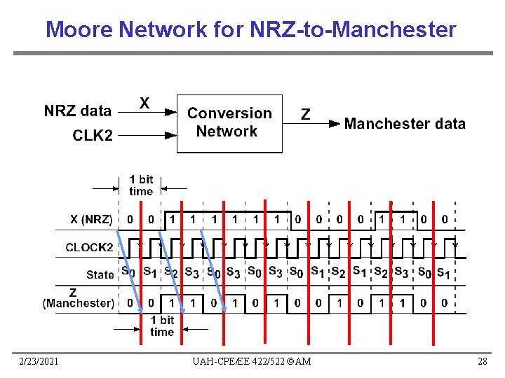
Moore Network for NRZ-to-Manchester 2/23/2021 UAH-CPE/EE 422/522 AM 28
Moore Network for NRZ-to-Manchester 2/23/2021 UAH-CPE/EE 422/522 AM 29
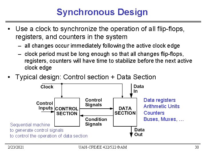
Synchronous Design • Use a clock to synchronize the operation of all flip-flops, registers, and counters in the system – all changes occur immediately following the active clock edge – clock period must be long enough so that all changes flip-flops, registers, counters will have time to stabilize before the next active clock edge • Typical design: Control section + Data Section Data registers Arithmetic Units Counters Buses, Muxes, … Sequential machine to generate control signals to control the operation of data section 2/23/2021 UAH-CPE/EE 422/522 AM 30
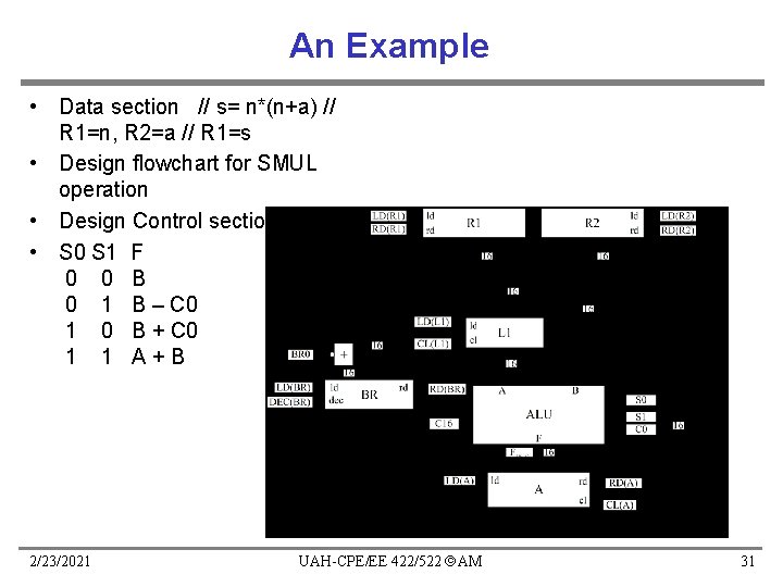
An Example • Data section // s= n*(n+a) // R 1=n, R 2=a // R 1=s • Design flowchart for SMUL operation • Design Control section • S 0 S 1 F 0 0 B 0 1 B – C 0 1 0 B + C 0 1 1 A+B 2/23/2021 UAH-CPE/EE 422/522 AM 31
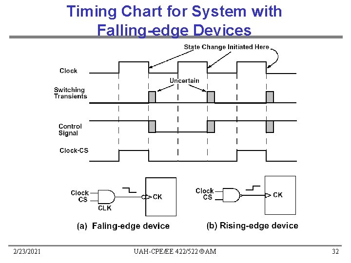
Timing Chart for System with Falling-edge Devices 2/23/2021 UAH-CPE/EE 422/522 AM 32
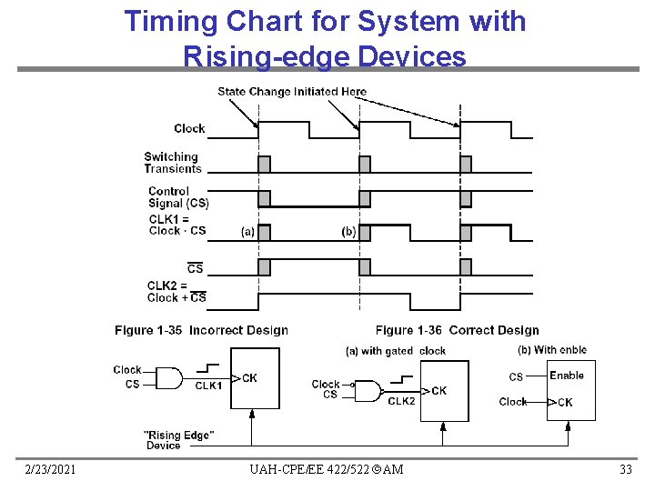
Timing Chart for System with Rising-edge Devices 2/23/2021 UAH-CPE/EE 422/522 AM 33
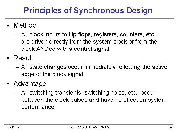
Principles of Synchronous Design • Method – All clock inputs to flip-flops, registers, counters, etc. , are driven directly from the system clock or from the clock ANDed with a control signal • Result – All state changes occur immediately following the active edge of the clock signal • Advantage – All switching transients, switching noise, etc. , occur between the clock pulses and have no effect on system performance 2/23/2021 UAH-CPE/EE 422/522 AM 34
Asynchronous Design • Disadvantage - More difficult – Problems • Race conditions: final state depends on the order in which variables change • Hazards – Special design techniques are needed to cope with races and hazards • Advantages = Disadvantages of Synchronous Design – In high-speed synchronous design propagation delay in wiring is significant => clock signal must be carefully routed so that it reaches all devices at essentially same time – Inputs are not synchronous with the clock – need for synchronizers – Clock cycle is determined by the worst-case delay 2/23/2021 UAH-CPE/EE 422/522 AM 35
To Do • Read – Textbook chapters 1. 6, 1. 7, 1. 8, 1. 10, 1. 11, 1. 12 2/23/2021 UAH-CPE/EE 422/522 AM 36