CPE 495 Computer Engineering Design I Introduction to
- Slides: 11

CPE 495 Computer Engineering Design I Introduction to PCB Design Emil Jovanov Electrical and Computer Engineering The University of Alabama in Huntsville CPE 495 Computer Engineering Design I, Dr. Emil Jovanov, UAH

Schematic Capture and PCB Design • Express. PCB schematic capture and PCB Design q http: //www. expresspcb. com/ Express. PCB software • Component selection q Through hole q SMT • Design for Test q Test points, grounds, etc. q Spare components CPE 495 Computer Engineering Design I, Dr. Emil Jovanov, UAH 2

Express. SCH • Express. PCB schematic capture q Quick Start Guide q examples • • New Schematic Component Manager Custom Components Wiring q Standard NET lists q Express. PCB integrated support • Sheets and Ports • Checking for Errors CPE 495 Computer Engineering Design I, Dr. Emil Jovanov, UAH 3

Express. PCB • Express. PCB design q Quick Start Guide q examples • Layers • Traces q Linking the Schematic and PCB • • • Grid Rules for Component Placement Ground plane Component Manager Custom components Ordering boards CPE 495 Computer Engineering Design I, Dr. Emil Jovanov, UAH 4

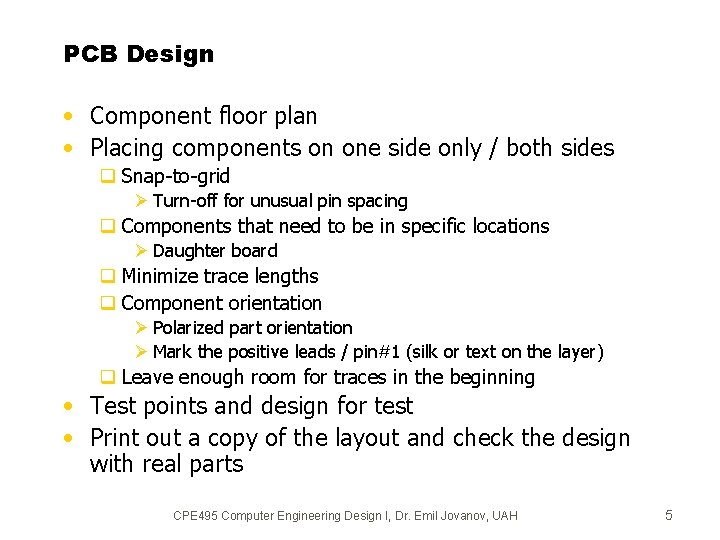
PCB Design • Component floor plan • Placing components on one side only / both sides q Snap-to-grid Ø Turn-off for unusual pin spacing q Components that need to be in specific locations Ø Daughter board q Minimize trace lengths q Component orientation Ø Polarized part orientation Ø Mark the positive leads / pin#1 (silk or text on the layer) q Leave enough room for traces in the beginning • Test points and design for test • Print out a copy of the layout and check the design with real parts CPE 495 Computer Engineering Design I, Dr. Emil Jovanov, UAH 5

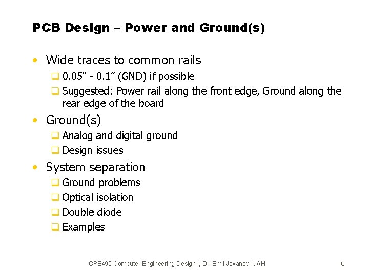
PCB Design – Power and Ground(s) • Wide traces to common rails q 0. 05” - 0. 1” (GND) if possible q Suggested: Power rail along the front edge, Ground along the rear edge of the board • Ground(s) q Analog and digital ground q Design issues • System separation q Ground problems q Optical isolation q Double diode q Examples CPE 495 Computer Engineering Design I, Dr. Emil Jovanov, UAH 6

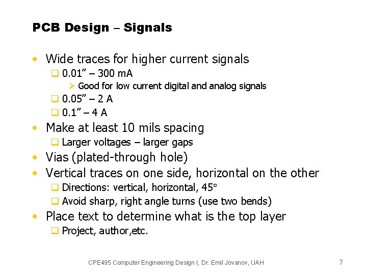
PCB Design – Signals • Wide traces for higher current signals q 0. 01” – 300 m. A Ø Good for low current digital and analog signals q 0. 05” – 2 A q 0. 1” – 4 A • Make at least 10 mils spacing q Larger voltages – larger gaps • Vias (plated-through hole) • Vertical traces on one side, horizontal on the other q Directions: vertical, horizontal, 45 q Avoid sharp, right angle turns (use two bends) • Place text to determine what is the top layer q Project, author, etc. CPE 495 Computer Engineering Design I, Dr. Emil Jovanov, UAH 7

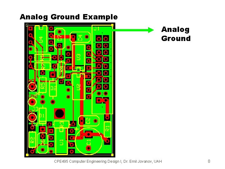
Analog Ground Example Analog Ground CPE 495 Computer Engineering Design I, Dr. Emil Jovanov, UAH 8

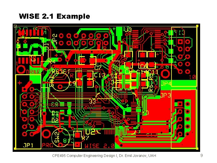
WISE 2. 1 Example CPE 495 Computer Engineering Design I, Dr. Emil Jovanov, UAH 9

Custom components • Custom components in SCH and PCB • Libraries q Sharing the same libraries q Team work CPE 495 Computer Engineering Design I, Dr. Emil Jovanov, UAH 10

Verification • Print and check component layout • Double check the routing of every signal q Use highlighter • Check for missing vias q Print separate layers Ø check for traces with dead-ends (not connected) Ø Check for traces that cross each other • Check for metal components (heat sinks, crystals, etc. ) that can cause shorts • Ordering boards CPE 495 Computer Engineering Design I, Dr. Emil Jovanov, UAH 11