CPE 169 Digital Design Laboratory Experiment 2 Introduction

CPE 169 Digital Design Laboratory Experiment #2: Introduction to Logic Functions and their Gate-Level Hardware Implementations
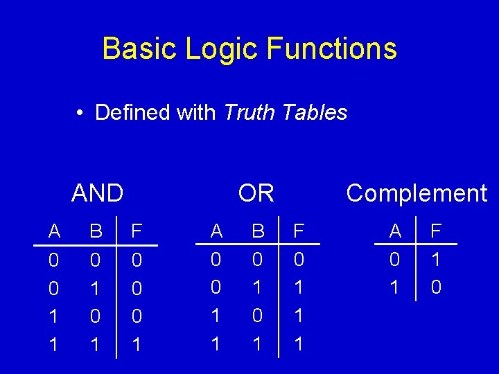
Basic Logic Functions • Defined with Truth Tables AND A 0 0 1 1 B 0 1 OR F 0 0 0 1 A 0 0 1 1 B 0 1 Complement F 0 1 1 1 A 0 1 F 1 0
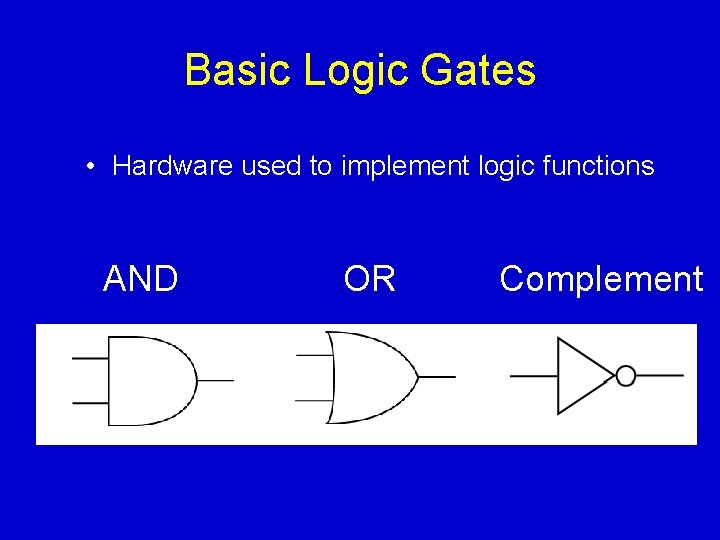
Basic Logic Gates • Hardware used to implement logic functions AND OR Complement
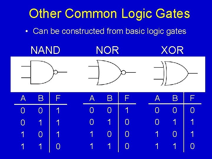
Other Common Logic Gates • Can be constructed from basic logic gates NAND A 0 0 1 1 B 0 1 F 1 1 1 0 NOR A 0 0 1 1 B 0 1 XOR F 1 0 0 0 A 0 0 1 1 B 0 1 F 0 1 1 0
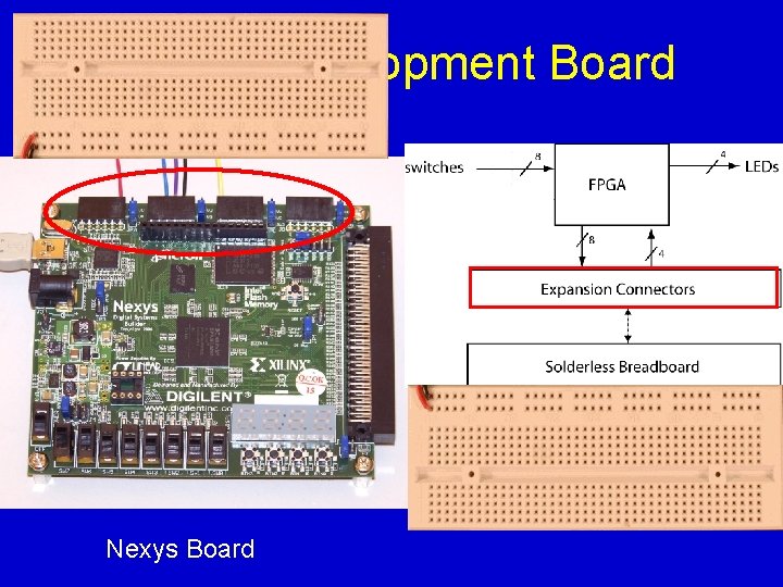
Nexys Development Board Nexys Board
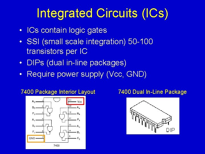
Integrated Circuits (ICs) • ICs contain logic gates • SSI (small scale integration) 50 -100 transistors per IC • DIPs (dual in-line packages) • Require power supply (Vcc, GND) 7400 Package Interior Layout 7400 Dual In-Line Package
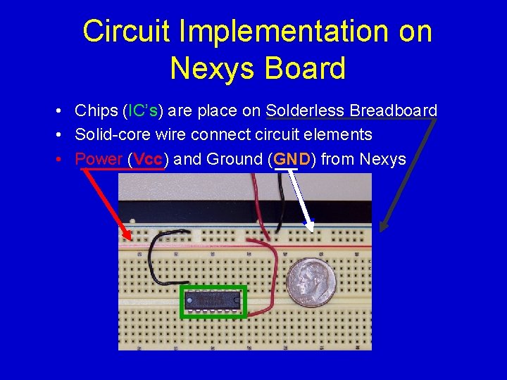
Circuit Implementation on Nexys Board • Chips (IC’s) are place on Solderless Breadboard • Solid-core wire connect circuit elements • Power (Vcc) and Ground (GND) from Nexys
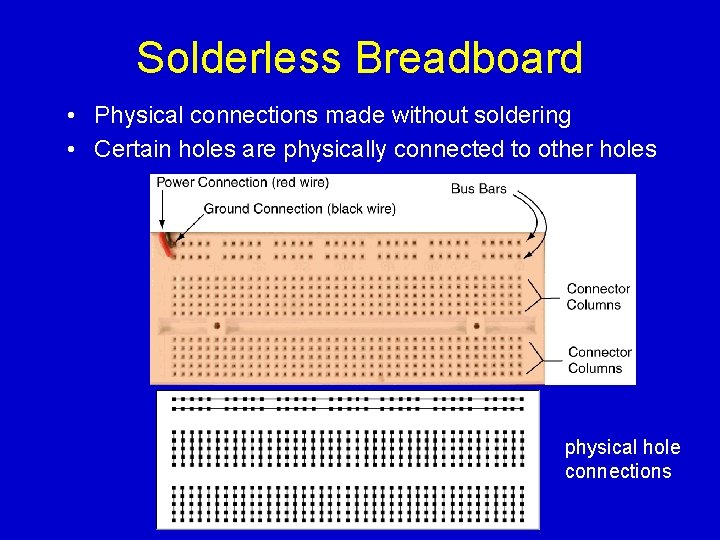
Solderless Breadboard • Physical connections made without soldering • Certain holes are physically connected to other holes physical hole connections
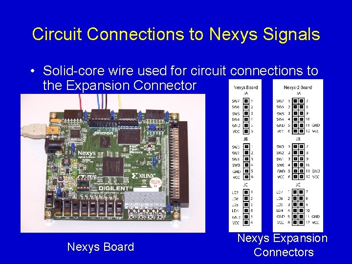
Circuit Connections to Nexys Signals • Solid-core wire used for circuit connections to the Expansion Connector Nexys Board Nexys Expansion Connectors
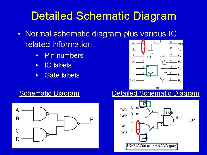
Detailed Schematic Diagram • Normal schematic diagram plus various IC related information: • Pin numbers • IC labels • Gate labels Schematic Diagram Detailed Schematic Diagram
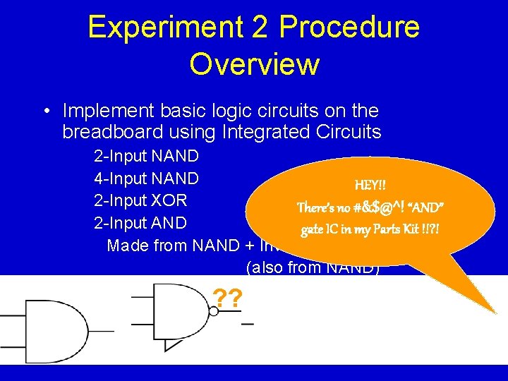
Experiment 2 Procedure Overview • Implement basic logic circuits on the breadboard using Integrated Circuits 2 -Input NAND 4 -Input NAND HEY!! 2 -Input XOR There’s no #&$@^! “AND” 2 -Input AND gate IC in my Parts Kit !!? ! Made from NAND + Inverter (also from NAND) • Verify your hardware ? ? implementations of each logic function.
- Slides: 11