Cp E 442 Memory System CPE 442 memory
- Slides: 37

Cp. E 442 Memory System CPE 442 memory. 1 Introduction To Computer Architecture

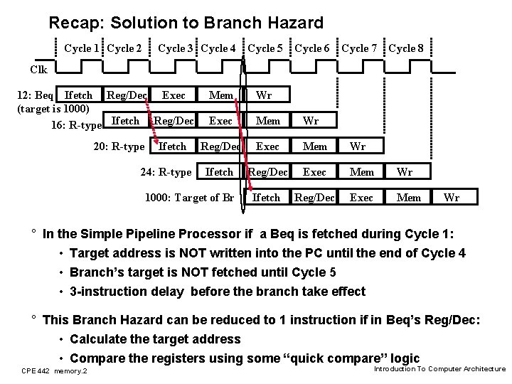
Recap: Solution to Branch Hazard Cycle 1 Cycle 2 Cycle 3 Cycle 4 Cycle 5 Cycle 6 Cycle 7 Cycle 8 Clk 12: Beq Ifetch Reg/Dec Exec (target is 1000) 16: R-type Ifetch Reg/Dec 20: R-type Ifetch 24: R-type Mem Wr Exec Mem Wr Reg/Dec Exec Mem Wr Ifetch Reg/Dec Exec Mem 1000: Target of Br Wr ° In the Simple Pipeline Processor if a Beq is fetched during Cycle 1: • Target address is NOT written into the PC until the end of Cycle 4 • Branch’s target is NOT fetched until Cycle 5 • 3 -instruction delay before the branch take effect ° This Branch Hazard can be reduced to 1 instruction if in Beq’s Reg/Dec: • Calculate the target address • Compare the registers using some “quick compare” logic CPE 442 memory. 2 Introduction To Computer Architecture

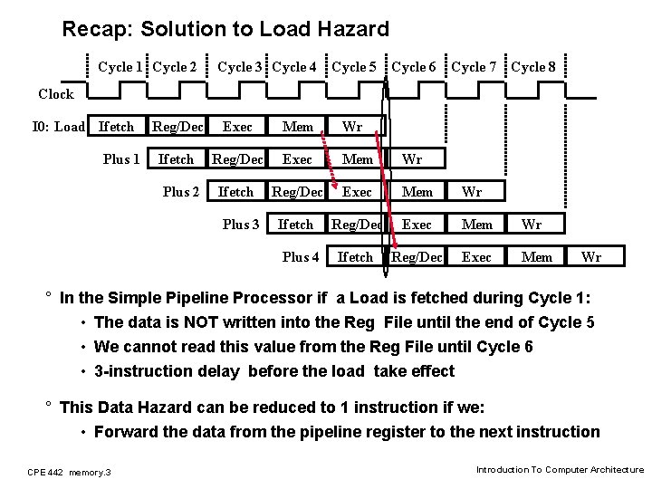
Recap: Solution to Load Hazard Cycle 1 Cycle 2 Cycle 3 Cycle 4 Cycle 5 Cycle 6 Cycle 7 Cycle 8 Clock I 0: Load Ifetch Plus 1 Reg/Dec Exec Mem Wr Ifetch Reg/Dec Exec Mem Plus 2 Plus 3 Plus 4 Wr ° In the Simple Pipeline Processor if a Load is fetched during Cycle 1: • The data is NOT written into the Reg File until the end of Cycle 5 • We cannot read this value from the Reg File until Cycle 6 • 3 -instruction delay before the load take effect ° This Data Hazard can be reduced to 1 instruction if we: • Forward the data from the pipeline register to the next instruction CPE 442 memory. 3 Introduction To Computer Architecture

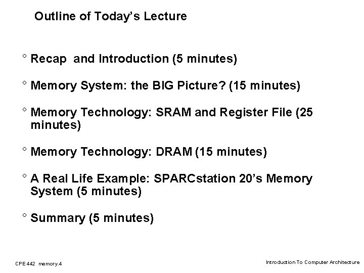
Outline of Today’s Lecture ° Recap and Introduction (5 minutes) ° Memory System: the BIG Picture? (15 minutes) ° Memory Technology: SRAM and Register File (25 minutes) ° Memory Technology: DRAM (15 minutes) ° A Real Life Example: SPARCstation 20’s Memory System (5 minutes) ° Summary (5 minutes) CPE 442 memory. 4 Introduction To Computer Architecture

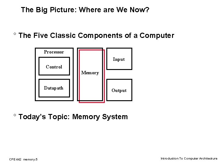
The Big Picture: Where are We Now? ° The Five Classic Components of a Computer Processor Input Control Memory Datapath Output ° Today’s Topic: Memory System CPE 442 memory. 5 Introduction To Computer Architecture

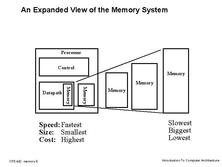
An Expanded View of the Memory System Processor Control Memory Datapath Speed: Fastest Size: Smallest Cost: Highest CPE 442 memory. 6 Memory Slowest Biggest Lowest Introduction To Computer Architecture

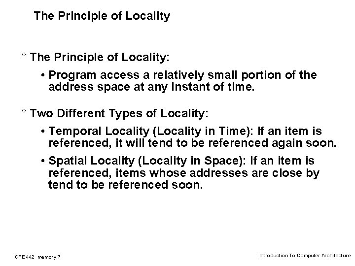
The Principle of Locality ° The Principle of Locality: • Program access a relatively small portion of the address space at any instant of time. ° Two Different Types of Locality: • Temporal Locality (Locality in Time): If an item is referenced, it will tend to be referenced again soon. • Spatial Locality (Locality in Space): If an item is referenced, items whose addresses are close by tend to be referenced soon. CPE 442 memory. 7 Introduction To Computer Architecture

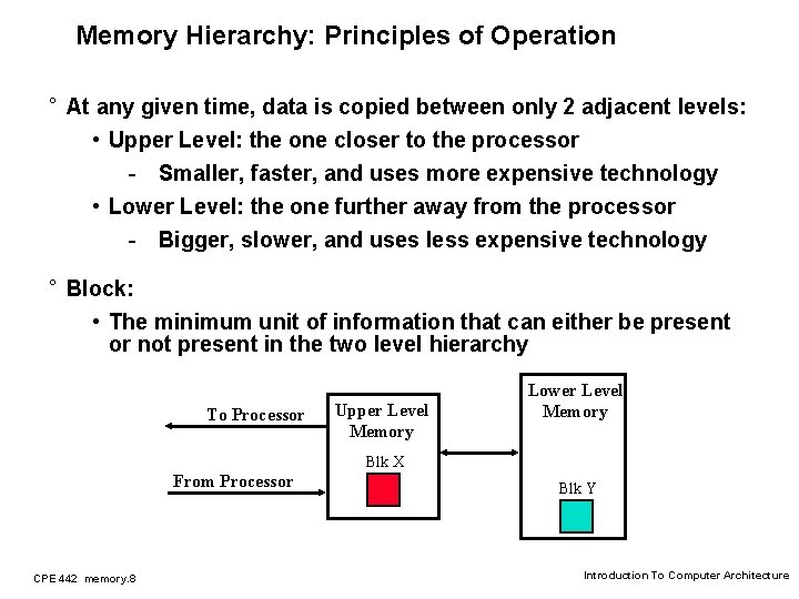
Memory Hierarchy: Principles of Operation ° At any given time, data is copied between only 2 adjacent levels: • Upper Level: the one closer to the processor - Smaller, faster, and uses more expensive technology • Lower Level: the one further away from the processor - Bigger, slower, and uses less expensive technology ° Block: • The minimum unit of information that can either be present or not present in the two level hierarchy To Processor Upper Level Memory Lower Level Memory Blk X From Processor CPE 442 memory. 8 Blk Y Introduction To Computer Architecture

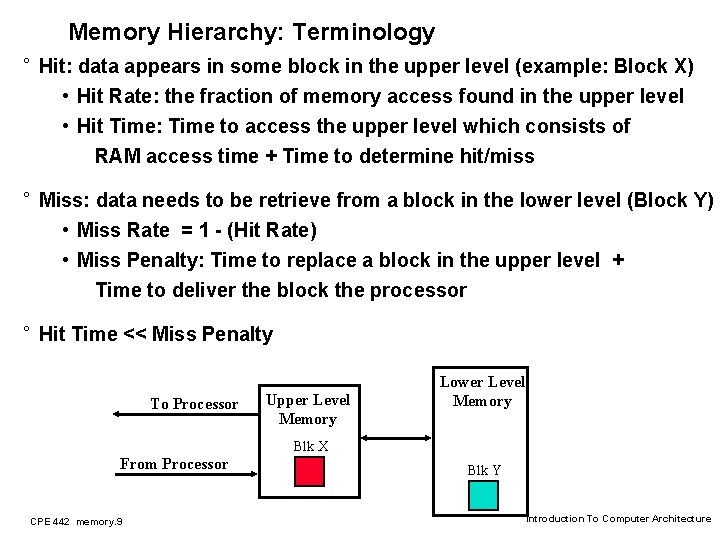
Memory Hierarchy: Terminology ° Hit: data appears in some block in the upper level (example: Block X) • Hit Rate: the fraction of memory access found in the upper level • Hit Time: Time to access the upper level which consists of RAM access time + Time to determine hit/miss ° Miss: data needs to be retrieve from a block in the lower level (Block Y) • Miss Rate = 1 - (Hit Rate) • Miss Penalty: Time to replace a block in the upper level + Time to deliver the block the processor ° Hit Time << Miss Penalty To Processor Upper Level Memory Lower Level Memory Blk X From Processor CPE 442 memory. 9 Blk Y Introduction To Computer Architecture

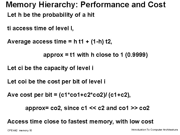
Memory Hierarchy: Performance and Cost Let h be the probability of a hit ti access time of level I, Average access time = h t 1 + (1 -h) t 2, approx = t 1 with h close to 1 (0. 9999) Let ci be the capacity of level i Let coi be the cost per bit of level i Ave cost per bit = (c 1*co 1+c 2*co 2)/ (c 1+c 2), approx= co 2, since c 1 << c 2 and co 1 >> co 2 Access time close to fastest memory, with low cost CPE 442 memory. 10 Introduction To Computer Architecture

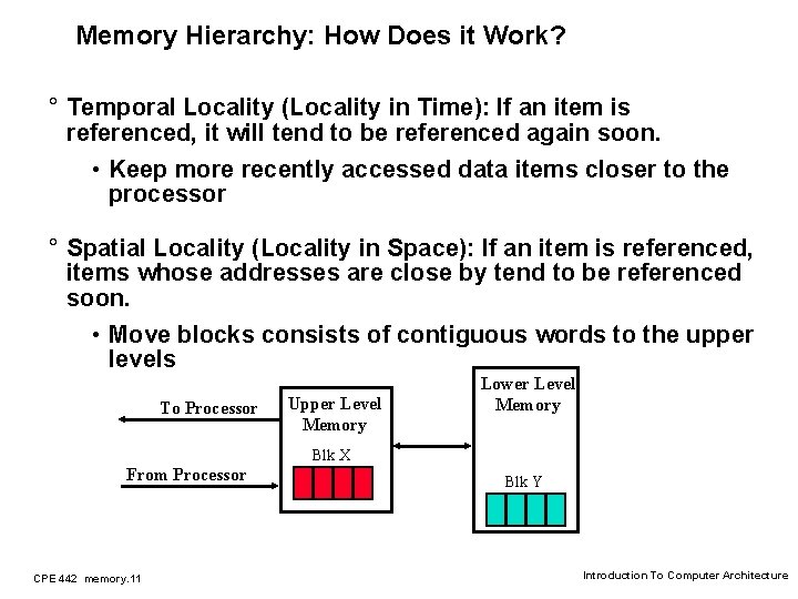
Memory Hierarchy: How Does it Work? ° Temporal Locality (Locality in Time): If an item is referenced, it will tend to be referenced again soon. • Keep more recently accessed data items closer to the processor ° Spatial Locality (Locality in Space): If an item is referenced, items whose addresses are close by tend to be referenced soon. • Move blocks consists of contiguous words to the upper levels To Processor Upper Level Memory Lower Level Memory Blk X From Processor CPE 442 memory. 11 Blk Y Introduction To Computer Architecture

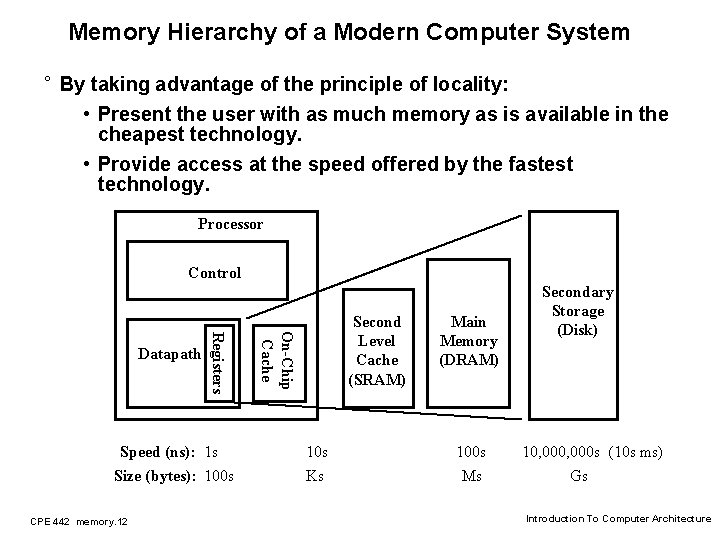
Memory Hierarchy of a Modern Computer System ° By taking advantage of the principle of locality: • Present the user with as much memory as is available in the cheapest technology. • Provide access at the speed offered by the fastest technology. Processor Control Speed (ns): 1 s Size (bytes): 100 s CPE 442 memory. 12 On-Chip Cache Registers Datapath Second Level Cache (SRAM) 10 s Ks Main Memory (DRAM) 100 s Ms Secondary Storage (Disk) 10, 000 s (10 s ms) Gs Introduction To Computer Architecture

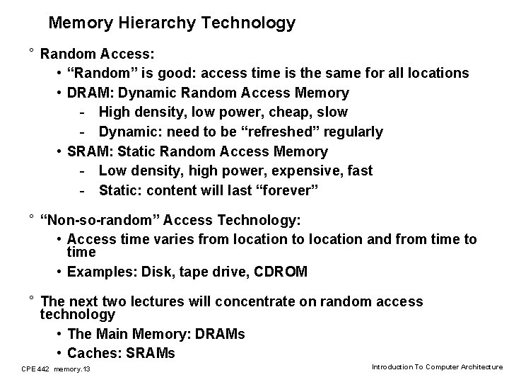
Memory Hierarchy Technology ° Random Access: • “Random” is good: access time is the same for all locations • DRAM: Dynamic Random Access Memory - High density, low power, cheap, slow - Dynamic: need to be “refreshed” regularly • SRAM: Static Random Access Memory - Low density, high power, expensive, fast - Static: content will last “forever” ° “Non-so-random” Access Technology: • Access time varies from location to location and from time to time • Examples: Disk, tape drive, CDROM ° The next two lectures will concentrate on random access technology • The Main Memory: DRAMs • Caches: SRAMs CPE 442 memory. 13 Introduction To Computer Architecture

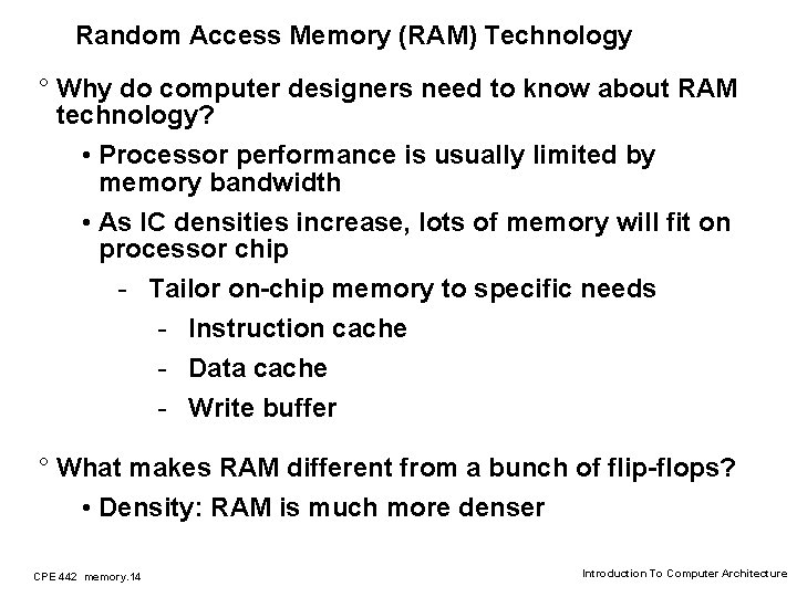
Random Access Memory (RAM) Technology ° Why do computer designers need to know about RAM technology? • Processor performance is usually limited by memory bandwidth • As IC densities increase, lots of memory will fit on processor chip - Tailor on-chip memory to specific needs - Instruction cache - Data cache - Write buffer ° What makes RAM different from a bunch of flip-flops? • Density: RAM is much more denser CPE 442 memory. 14 Introduction To Computer Architecture

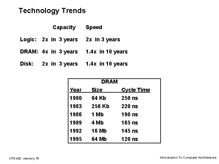
Technology Trends Capacity Logic: 2 x in 3 years Speed 2 x in 3 years DRAM: 4 x in 3 years 1. 4 x in 10 years Disk: 1. 4 x in 10 years 2 x in 3 years DRAM CPE 442 memory. 15 Year 1980 1983 1986 Size 64 Kb 256 Kb 1 Mb Cycle Time 250 ns 220 ns 1989 1992 1995 4 Mb 16 Mb 64 Mb 165 ns 145 ns 120 ns Introduction To Computer Architecture

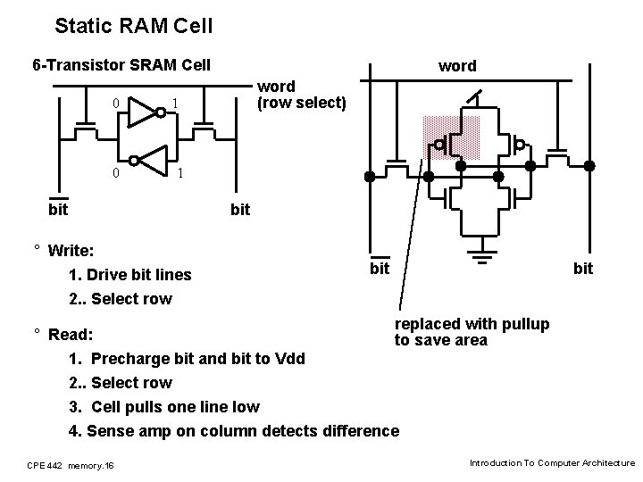
Static RAM Cell 6 -Transistor SRAM Cell 0 0 word (row select) 1 1 bit ° Write: 1. Drive bit lines 2. . Select row bit bit replaced with pullup ° Read: to save area 1. Precharge bit and bit to Vdd 2. . Select row 3. Cell pulls one line low 4. Sense amp on column detects difference CPE 442 memory. 16 Introduction To Computer Architecture

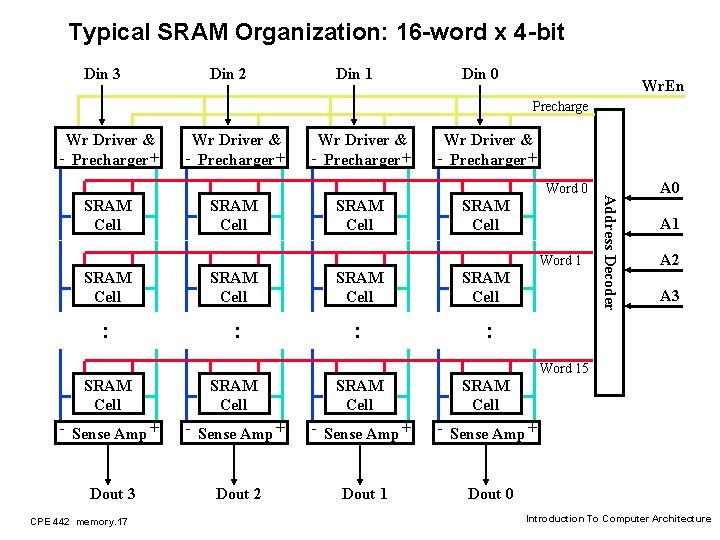
Typical SRAM Organization: 16 -word x 4 -bit Din 3 Din 2 Din 1 Din 0 Wr. En Precharge Wr Driver & - Precharger + SRAM Cell Word 1 SRAM Cell : : Address Decoder Word 0 A 1 A 2 A 3 Word 15 SRAM Cell - Sense Amp + Dout 3 Dout 2 Dout 1 Dout 0 CPE 442 memory. 17 Introduction To Computer Architecture

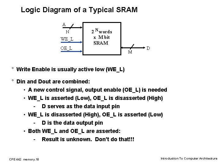
Logic Diagram of a Typical SRAM A N WE_L OE_L 2 N words x M bit SRAM M D ° Write Enable is usually active low (WE_L) ° Din and Dout are combined: • A new control signal, output enable (OE_L) is needed • WE_L is asserted (Low), OE_L is disasserted (High) - D serves as the data input pin • WE_L is disasserted (High), OE_L is asserted (Low) - D is the data output pin • Both WE_L and OE_L are asserted: - Result is unknown. Don’t do that!!! CPE 442 memory. 18 Introduction To Computer Architecture

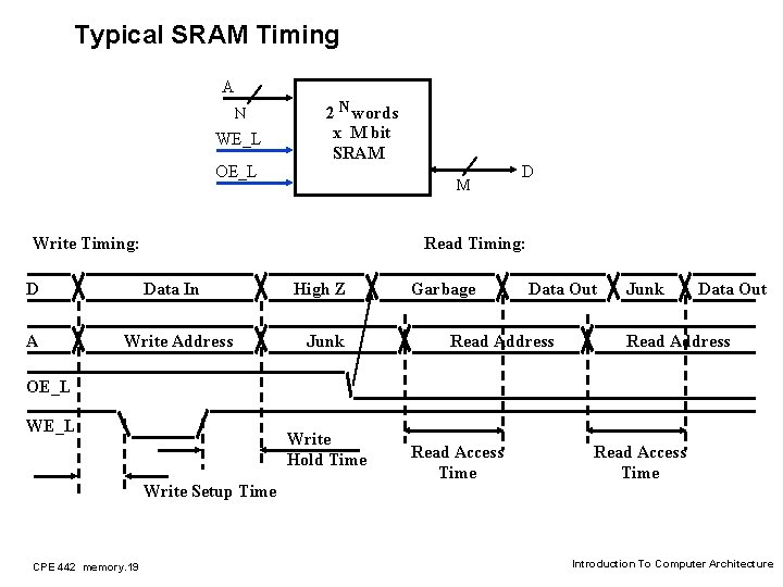
Typical SRAM Timing A N WE_L OE_L 2 N words x M bit SRAM M Write Timing: D A D Read Timing: Data In Write Address High Z Junk Garbage Data Out Read Address Junk Data Out Read Address OE_L Write Hold Time Write Setup Time CPE 442 memory. 19 Read Access Time Introduction To Computer Architecture

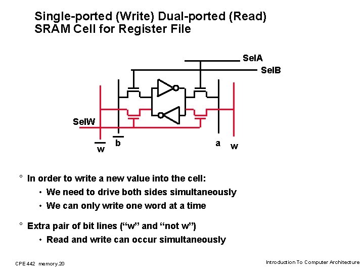
Single-ported (Write) Dual-ported (Read) SRAM Cell for Register File Sel. A Sel. B Sel. W w b a w ° In order to write a new value into the cell: • We need to drive both sides simultaneously • We can only write one word at a time ° Extra pair of bit lines (“w” and “not w”) • Read and write can occur simultaneously CPE 442 memory. 20 Introduction To Computer Architecture

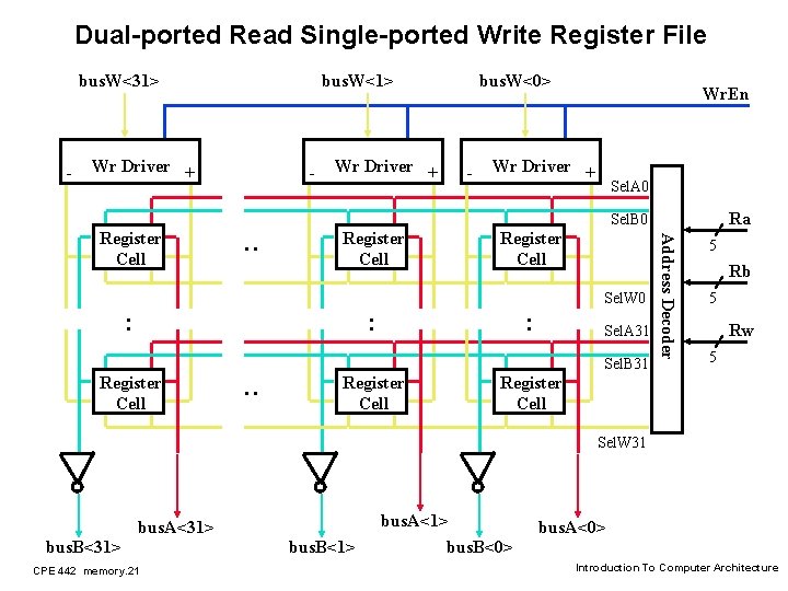
Dual-ported Read Single-ported Write Register File bus. W<31> - bus. W<1> Wr Driver + - Wr Driver + bus. W<0> - Wr. En Wr Driver + Sel. A 0 Ra Register Cell Sel. W 0 : : : Sel. A 31 Register Cell : Sel. B 31 Register Cell Address Decoder Register Cell : Sel. B 0 5 Rb 5 Rw 5 Register Cell Sel. W 31 bus. A<31> bus. B<31> CPE 442 memory. 21 bus. B<1> bus. A<1> bus. B<0> bus. A<0> Introduction To Computer Architecture

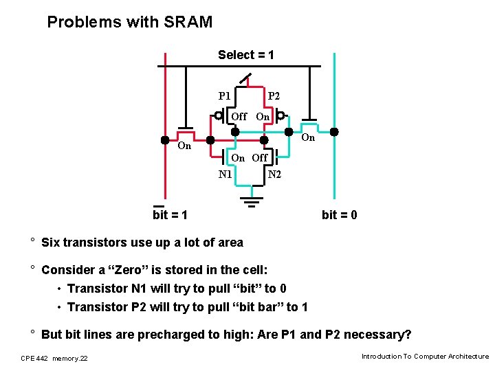
Problems with SRAM Select = 1 P 2 Off On On Off N 1 N 2 bit = 1 bit = 0 ° Six transistors use up a lot of area ° Consider a “Zero” is stored in the cell: • Transistor N 1 will try to pull “bit” to 0 • Transistor P 2 will try to pull “bit bar” to 1 ° But bit lines are precharged to high: Are P 1 and P 2 necessary? CPE 442 memory. 22 Introduction To Computer Architecture

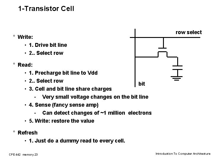
1 -Transistor Cell ° Write: • 1. Drive bit line • 2. . Select row select ° Read: • 1. Precharge bit line to Vdd • 2. . Select row bit • 3. Cell and bit line share charges - Very small voltage changes on the bit line • 4. Sense (fancy sense amp) - Can detect changes of ~1 million electrons • 5. Write: restore the value ° Refresh • 1. Just do a dummy read to every cell. CPE 442 memory. 23 Introduction To Computer Architecture

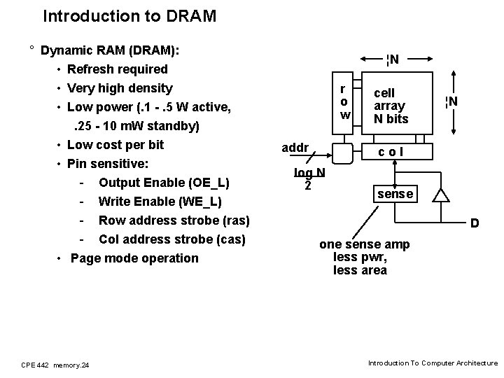
Introduction to DRAM ° Dynamic RAM (DRAM): • Refresh required • Very high density • Low power (. 1 -. 5 W active, . 25 - 10 m. W standby) • Low cost per bit • Pin sensitive: - Output Enable (OE_L) - Write Enable (WE_L) - Row address strobe (ras) - Col address strobe (cas) • Page mode operation CPE 442 memory. 24 ¦N r o w addr cell array N bits ¦N col log N 2 sense D one sense amp less pwr, less area Introduction To Computer Architecture

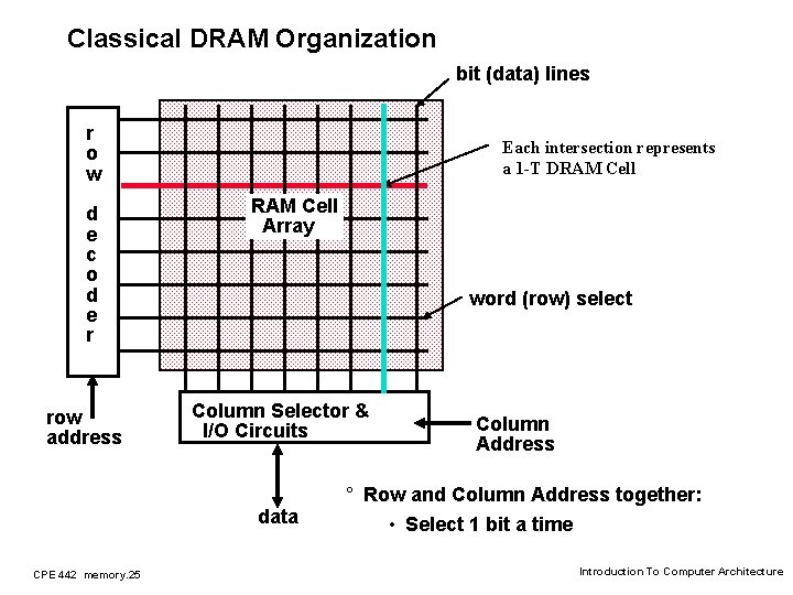
Classical DRAM Organization bit (data) lines r o w d e c o d e r row address Each intersection represents a 1 -T DRAM Cell Array word (row) select Column Selector & I/O Circuits data CPE 442 memory. 25 Column Address ° Row and Column Address together: • Select 1 bit a time Introduction To Computer Architecture

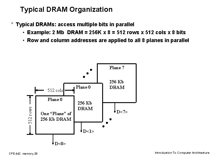
Typical DRAM Organization ° Typical DRAMs: access multiple bits in parallel • Example: 2 Mb DRAM = 256 K x 8 = 512 rows x 512 cols x 8 bits • Row and column addresses are applied to all 8 planes in parallel Plane 7 512 cols 512 rows Plane 0 One “Plane” of 256 Kb DRAM Plane 0 256 Kb DRAM D<7> D<1> D<0> CPE 442 memory. 26 Introduction To Computer Architecture

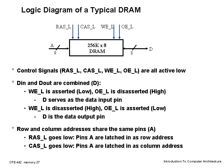
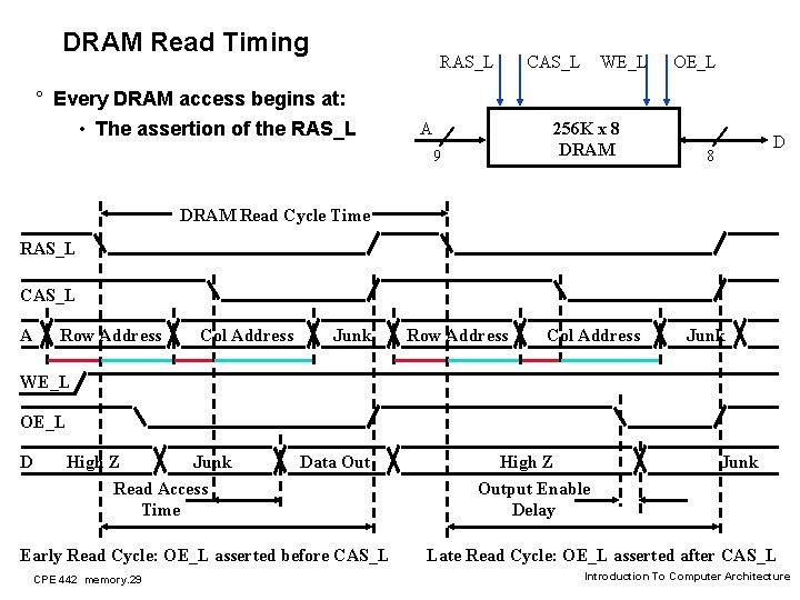
Logic Diagram of a Typical DRAM RAS_L A 9 CAS_L WE_L 256 K x 8 DRAM OE_L 8 D ° Control Signals (RAS_L, CAS_L, WE_L, OE_L) are all active low ° Din and Dout are combined (D): • WE_L is asserted (Low), OE_L is disasserted (High) - D serves as the data input pin • WE_L is disasserted (High), OE_L is asserted (Low) - D is the data output pin ° Row and column addresses share the same pins (A) • RAS_L goes low: Pins A are latched in as row address • CAS_L goes low: Pins A are latched in as column address CPE 442 memory. 27 Introduction To Computer Architecture

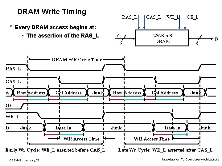
DRAM Write Timing RAS_L ° Every DRAM access begins at: • The assertion of the RAS_L A CAS_L WE_L 256 K x 8 DRAM 9 OE_L D 8 DRAM WR Cycle Time RAS_L CAS_L A Row Address Col Address Junk OE_L WE_L D Junk Data In WR Access Time Early Wr Cycle: WE_L asserted before CAS_L CPE 442 memory. 28 Junk Data In Junk WR Access Time Late Wr Cycle: WE_L asserted after CAS_L Introduction To Computer Architecture

DRAM Read Timing RAS_L ° Every DRAM access begins at: • The assertion of the RAS_L A CAS_L WE_L 256 K x 8 DRAM 9 OE_L D 8 DRAM Read Cycle Time RAS_L CAS_L A Row Address Col Address Junk WE_L OE_L D High Z Junk Read Access Time Data Out Early Read Cycle: OE_L asserted before CAS_L CPE 442 memory. 29 High Z Output Enable Delay Junk Late Read Cycle: OE_L asserted after CAS_L Introduction To Computer Architecture

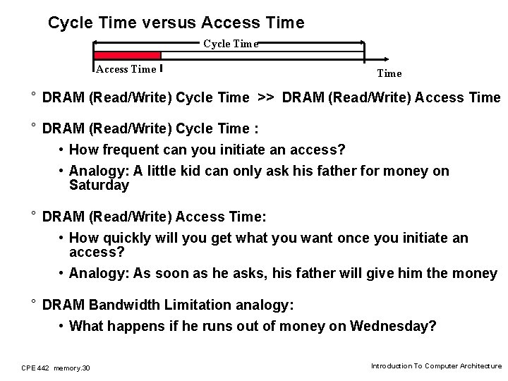
Cycle Time versus Access Time Cycle Time Access Time ° DRAM (Read/Write) Cycle Time >> DRAM (Read/Write) Access Time ° DRAM (Read/Write) Cycle Time : • How frequent can you initiate an access? • Analogy: A little kid can only ask his father for money on Saturday ° DRAM (Read/Write) Access Time: • How quickly will you get what you want once you initiate an access? • Analogy: As soon as he asks, his father will give him the money ° DRAM Bandwidth Limitation analogy: • What happens if he runs out of money on Wednesday? CPE 442 memory. 30 Introduction To Computer Architecture

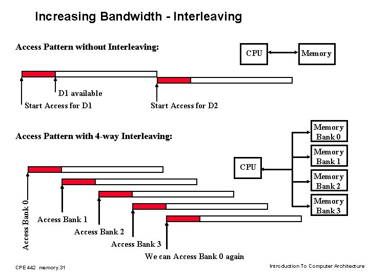
Increasing Bandwidth - Interleaving Access Pattern without Interleaving: D 1 available Start Access for D 1 CPU Memory Start Access for D 2 Memory Bank 0 Access Pattern with 4 -way Interleaving: CPU Memory Bank 1 Access Bank 0 Memory Bank 2 Access Bank 1 Access Bank 2 Access Bank 3 We can Access Bank 0 again CPE 442 memory. 31 Memory Bank 3 Introduction To Computer Architecture

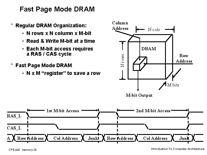
Fast Page Mode DRAM ° Fast Page Mode DRAM • N x M “register” to save a row Column Address N cols DRAM Row Address N rows ° Regular DRAM Organization: • N rows x N column x M-bit • Read & Write M-bit at a time • Each M-bit access requires a RAS / CAS cycle M bits M-bit Output 1 st M-bit Access 2 nd M-bit Access RAS_L CAS_L A Row Address CPE 442 memory. 32 Col Address Junk Row Address Col Address Junk Introduction To Computer Architecture

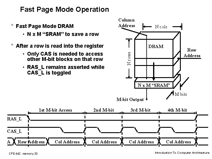
Fast Page Mode Operation ° After a row is read into the register • Only CAS is needed to access other M-bit blocks on that row • RAS_L remains asserted while CAS_L is toggled N cols DRAM Row Address N rows ° Fast Page Mode DRAM • N x M “SRAM” to save a row Column Address N x M “SRAM” M bits M-bit Output 1 st M-bit Access 2 nd M-bit 3 rd M-bit 4 th M-bit Col Address RAS_L CAS_L A Row Address CPE 442 memory. 33 Col Address Introduction To Computer Architecture

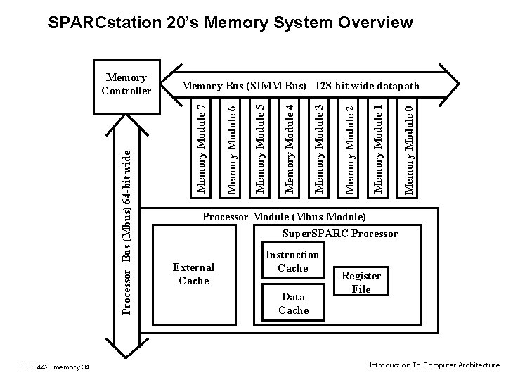
SPARCstation 20’s Memory System Overview CPE 442 memory. 34 Memory Module 0 Memory Module 1 Memory Module 2 Memory Module 3 Memory Module 4 Memory Module 5 Memory Module 6 Memory Bus (SIMM Bus) 128 -bit wide datapath Memory Module 7 Processor Bus (Mbus) 64 -bit wide Memory Controller Processor Module (Mbus Module) Super. SPARC Processor External Cache Instruction Cache Data Cache Register File Introduction To Computer Architecture

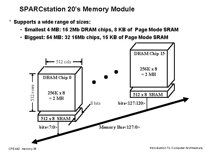
SPARCstation 20’s Memory Module ° Supports a wide range of sizes: • Smallest 4 MB: 16 2 Mb DRAM chips, 8 KB of Page Mode SRAM • Biggest: 64 MB: 32 16 Mb chips, 16 KB of Page Mode SRAM DRAM Chip 15 512 cols 256 K x 8 = 2 MB 512 rows DRAM Chip 0 256 K x 8 = 2 MB 512 x 8 SRAM 8 bits<127: 120> 512 x 8 SRAM bits<7: 0> CPE 442 memory. 35 Memory Bus<127: 0> Introduction To Computer Architecture

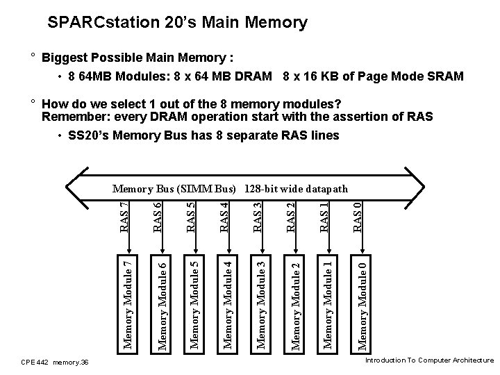
SPARCstation 20’s Main Memory ° Biggest Possible Main Memory : • 8 64 MB Modules: 8 x 64 MB DRAM 8 x 16 KB of Page Mode SRAM ° How do we select 1 out of the 8 memory modules? Remember: every DRAM operation start with the assertion of RAS • SS 20’s Memory Bus has 8 separate RAS lines CPE 442 memory. 36 RAS 0 Memory Module 0 RAS 1 Memory Module 1 RAS 2 Memory Module 2 RAS 3 Memory Module 3 RAS 4 Memory Module 4 RAS 5 Memory Module 5 RAS 6 Memory Module 7 RAS 7 Memory Bus (SIMM Bus) 128 -bit wide datapath Introduction To Computer Architecture

Summary: ° Two Different Types of Locality: • Temporal Locality (Locality in Time): If an item is referenced, it will tend to be referenced again soon. • Spatial Locality (Locality in Space): If an item is referenced, items whose addresses are close by tend to be referenced soon. ° By taking advantage of the principle of locality: • Present the user with as much memory as is available in the cheapest technology. • Provide access at the speed offered by the fastest technology. ° DRAM is slow but cheap and dense: • Good choice for presenting the user with a BIG memory system ° SRAM is fast but expensive and not very dense: • Good choice for providing the user FAST access time. CPE 442 memory. 37 Introduction To Computer Architecture