COURSE OUTCOMES OF MICROPROCESSOR AND PROGRAMMING C 404


 CPU – Central Processing Unit Memory ROM –")
 Programmable integrated device (silicon chip) that has computing & decision making capabilities")


- Slides: 27
COURSE OUTCOMES OF MICROPROCESSOR AND PROGRAMMING C 404. 1 Describe the architecture and organization microprocessor along with instruction set format. C 404. 2 Describe modes and functional block diagram of 8086 along with pins and their functions C 404. 3 List and describe memory and addressing modes C 404. 4 List, describe and use different types of instructions, directives and interrupts C 404. 5 Develop assembly language programs using various programming tools. Visit for more Learning Resources of
CHAPTER 1 BASICS OF MICROPROCESSOR
ORGANIZATION OF A MICROPROCESSORBASED SYSTEM (COMPUTER) CPU – Central Processing Unit Memory ROM – Read Only Memory RAM – Random Access Memory I/O Keyboard Display Device Clock – Square Wave Oscillator (Timing) System Bus
Microprocessor (CPU) Programmable integrated device (silicon chip) that has computing & decision making capabilities Communicates & operates in binary numbers 0 & 1, called bits Has a fixed set of instructions in the form of binary patterns – machine language Difficult for humans to remember machine language – each instruction is represented using abbreviated names (mnemonics)
Memory Symbolic representation Word length 1 word instruction 2 word instruction n n address n Word: no. of bits micro-P recognizes and processes at a time ( 4 - 64 bit ). Instruction: combination of bit patterns with specific meaning known to micro-P. Program: Set of all instructions.
I/O Microprocessor’s Input: connection to the outside world Keyboard, mouse Output: Monitor, printer
System Bus – wires connecting memory & I/O to microprocessor Address Bus Unidirectional Identifying Data peripheral or memory location Bus Bidirectional Transferring Control data Bus Synchronization Timing signals Control signals
Actions performed by microprocessor: CPU – Memory CPU – I/O Data Processing Arithmetic operations Logical operations Control Jump Interrupts
BASIC CONCEPTS OF MICROPROCESSORS Differences between: Microcomputer – a computer with a microprocessor as its CPU. Includes memory, I/O etc. Microprocessor – silicon chip which includes ALU, register circuits & control circuits Microcontroller – silicon chip which includes microprocessor, memory & I/O in a single package.
Differences between: High level language Assembly language Machine language
ARCHITECTURE OF INTEL 8085 MICROPROCESSOR
INTEL 8085 MICROPROCESSOR Microprocessor consists of: Control unit: control microprocessor operations. ALU: performs data processing function. Registers: provide storage internal to CPU. Interrupts Internal data bus
Registers General Purpose Registers B, C, D, E, H & L (8 bit registers) Can be used singly Or can be used as 16 bit register pairs BC, DE, HL H & L can be used as a data pointer (holds memory address) Special Purpose Registers Accumulator (8 bit register) Store 8 bit data Store the result of an operation Store 8 bit data during I/O transfer
Flag Register 8 bit register – shows the status of the microprocessor before/after an operation S (sign flag), Z (zero flag), AC (auxillary carry flag), P (parity flag) & CY (carry flag) D 7 D 6 D 5 D 4 D 3 D 2 D 1 D 0 S Z X AC X P X CY Sign Flag Used for indicating the sign of the data in the accumulator The sign flag is set if negative (1 – negative) The sign flag is reset if positive (0 – positive)
Zero Flag Is set if result obtained after an operation is 0 Is set following an increment or decrement operation of that register Carry Flag 10110011 + 01001101 -------1 0000 Is set if there is a carry or borrow from arithmetic operation 1011 0101 + 0110 1100 -------Carry 1 0010 0001 1011 0101 - 1100 -------Borrow 1 1110 1001
Auxillary Carry Flag Is set if there is a carry out of bit 3 1011 0101 + 0110 1100 -------1 0010 0001 Parity Flag Is set if parity is even Is cleared if parity is odd
16 – Bit Registers Program Counter A pointer to the next instruction to be executed Contains the 16 -bit memory address of the next instruction Updated after processor has fetched the instruction Stack Pointer Stack – an area in memory in which temporary info is stored Stack – FILO (First In Last Out) basis Holds the address of the top of the stack
NON PROGRAMMABLE REGISTERS Instruction Register & Decoder Instruction is stored in IR after fetched by processor Decoder decodes instruction in IR Internal Clock generator 3. 125 MHz internally 6. 25 MHz externally
BASIC WORKING OF A MICROPROCESSOR Instructions are stored sequentially in memory Microprocessor Fetches instruction from memory Decodes instruction Executes instruction
INTERRUPTS OF 8085 MICROPROCESSOR Maskable Interrupts Microprocessor can ignore or delay interrupt request INTR – General purpose interrupt RST 5. 5, RST 6. 5, RST 7. 5 – Restart interrupts, higher priorities Nonmaskable Interrupts Enabled by default Cannot be disabled Microprocessor must respond to it immediately TRAP – highest priority
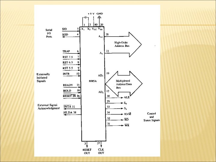
GROUPING OF SIGNALS OF 8085 MICROPROCESSOR Power supply and frequency signals Address bus signals Data bus signals Control and status signals Externally initiated signals & external signal acknowledgement Serial I/O port signals
ADDRESS BUS SIGNALS, DATA BUS SIGNALS AD 0 -AD 7, A 8 -A 15 16 address lines – 2 sets Most significant bits (A 8 -A 15) – single directional Least significant bits (AD 0 -AD 7) – bidirectional Multiplexed with the bits of bi-directional data bus It is used as both address and data bus
CONTROL AND STATUS SIGNALS Status_ lines: IO/M Differentiate I/O and memory applications High – I/O Low – Memory S 1, S 0 – status signals, to indicate the type of machine cycle in progress Control _ _lines: __ RD, WR & INTA RD – data on the data bus to be read into processor WR – data on the data bus to be written to processor INTA – acknowledge an INTR interrupt
EXTERNALLY INITIATED SIGNALS & SIGNAL ACKNOWLEDGEMENT Initiated signals Reset In – reset CPU Hold – suspend CPU operation Ready – CPU go into wait state, to sync with slower devices Signal acknowledgement Reset out – high once CPU is rest HLDA – acknowledges hold signal
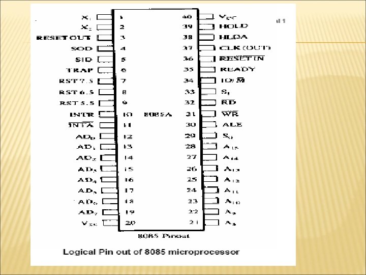
8085 PIN DIAGRAM For more detail contact us