COSE 221 COMP 211 Logic Design Lecture 6


![Verilog-HDL Representation module adder #(parameter N = (input [N-1: 0] input output [N-1: 0] Verilog-HDL Representation module adder #(parameter N = (input [N-1: 0] input output [N-1: 0]](https://slidetodoc.com/presentation_image_h/fc8b60684010c148f55315e9f3884dbb/image-24.jpg)

- Slides: 33

COSE 221, COMP 211 Logic Design Lecture 6. Adders Prof. Taeweon Suh Computer Science & Engineering Korea University

Introduction • So far, we have studied the basic skills of designing combinational and sequential logic using schematic and Verilog-HDL • Now, we are going to study some interesting combinational and sequential blocks, including § Arithmetic circuits: Adders and Subtractor § Counters § Shift Registers • Also, we are going to discuss how computer represents floatingpoint numbers § float and double in C langauge • The last topics to discuss are Memory and Logic Arrays 2 Korea Univ

Arithmetic Circuits • Computers are able to perform various arithmetic operations such as addition, subtraction, comparison, shift, multiplication, and division § Arithmetic circuits are the central building blocks of computers (CPUs) • We are going to study hardware implementations of these operations • Let’s start with adder • Addition is one of most common operations in computer 3 Korea Univ

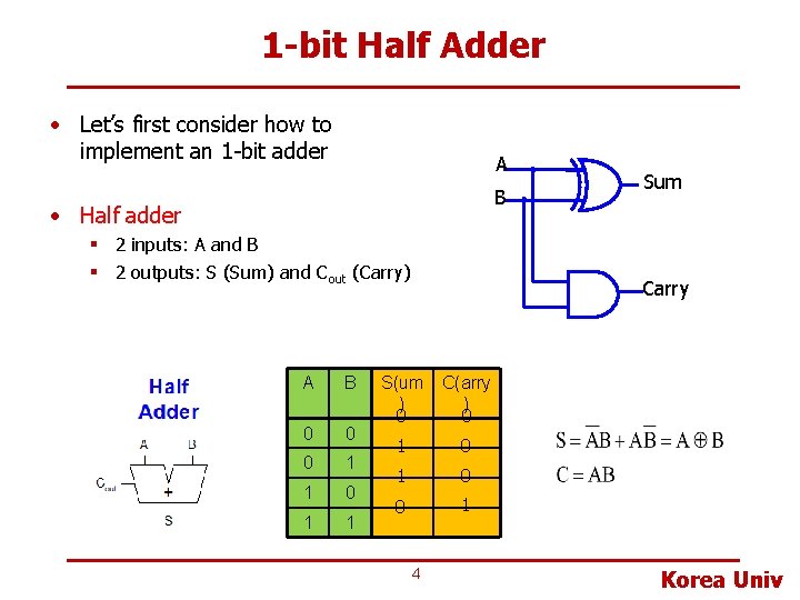
1 -bit Half Adder • Let’s first consider how to implement an 1 -bit adder A B • Half adder § 2 inputs: A and B § 2 outputs: S (Sum) and Cout (Carry) A B 0 0 0 1 1 Sum Carry S(um ) 0 C(arry ) 0 1 0 0 1 4 Korea Univ

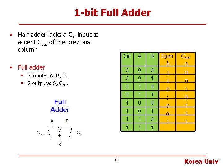
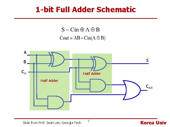
1 -bit Full Adder • Half adder lacks a Cin input to accept Cout of the previous column Cin • Full adder § 3 inputs: A, B, Cin § 2 outputs: S, Cout 5 A B 0 0 0 1 1 1 0 0 1 1 1 S(um ) 0 Cout 1 0 0 1 1 1 0 Korea Univ

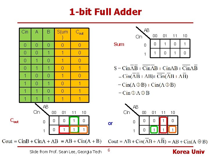
1 -bit Full Adder Cin A B S(um ) Cout 0 0 0 0 1 1 0 0 1 0 1 1 1 0 0 1 1 1 Cin Cout AB 00 01 11 10 0 0 1 1 1 0 00 01 11 10 0 1 0 1 1 1 Cin Sum AB 00 01 11 10 0 1 0 1 1 1 Slide from Prof. Sean Lee, Georgia Tech Cin or 6 AB Korea Univ

1 -bit Full Adder Schematic A S B Cin Half Adder Cout Slide from Prof. Sean Lee, Georgia Tech 7 Korea Univ

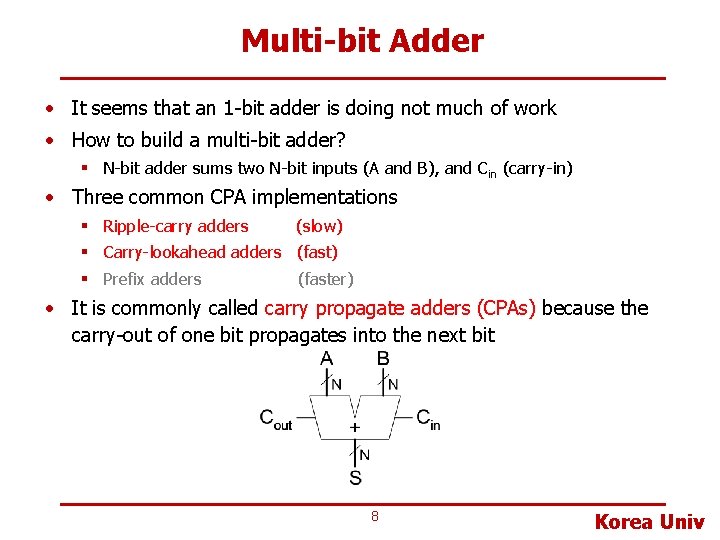
Multi-bit Adder • It seems that an 1 -bit adder is doing not much of work • How to build a multi-bit adder? § N-bit adder sums two N-bit inputs (A and B), and Cin (carry-in) • Three common CPA implementations § Ripple-carry adders (slow) § Carry-lookahead adders (fast) § Prefix adders (faster) • It is commonly called carry propagate adders (CPAs) because the carry-out of one bit propagates into the next bit 8 Korea Univ

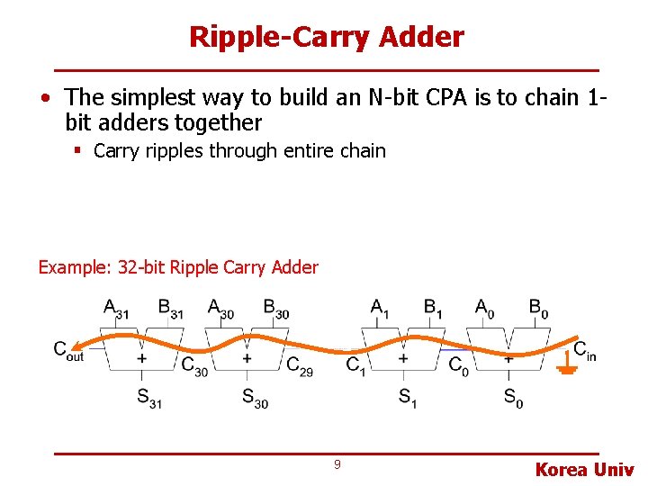
Ripple-Carry Adder • The simplest way to build an N-bit CPA is to chain 1 bit adders together § Carry ripples through entire chain Example: 32 -bit Ripple Carry Adder 9 Korea Univ

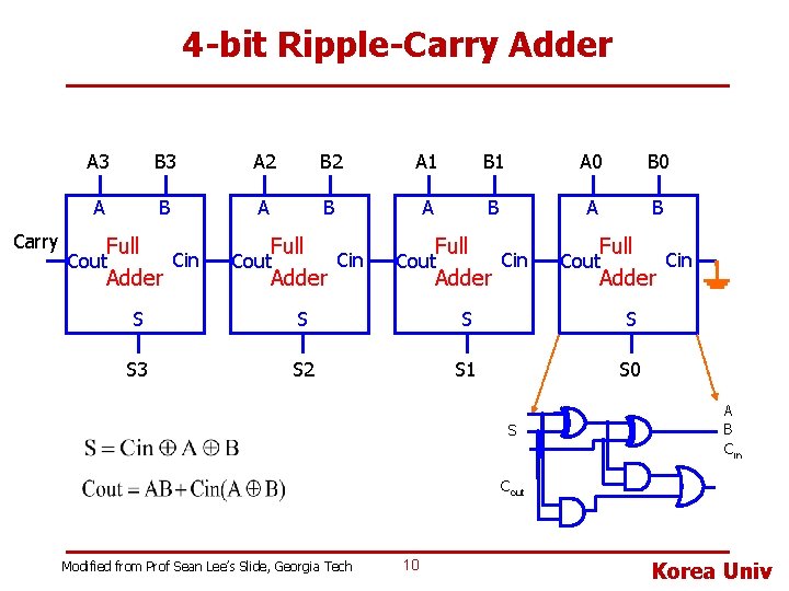
4 -bit Ripple-Carry Adder Carry A 3 B 3 A 2 B 2 A 1 B 1 A 0 B 0 A B A B Full Cin Adder Cout S S S 3 S 2 S 1 S 0 S A B Cin Cout Modified from Prof Sean Lee’s Slide, Georgia Tech 10 Korea Univ

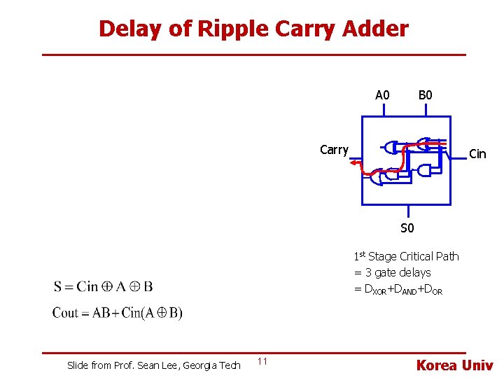
Delay of Ripple Carry Adder A 0 B 0 Carry Cin S 0 1 st Stage Critical Path = 3 gate delays = DXOR+DAND+DOR Slide from Prof. Sean Lee, Georgia Tech 11 Korea Univ

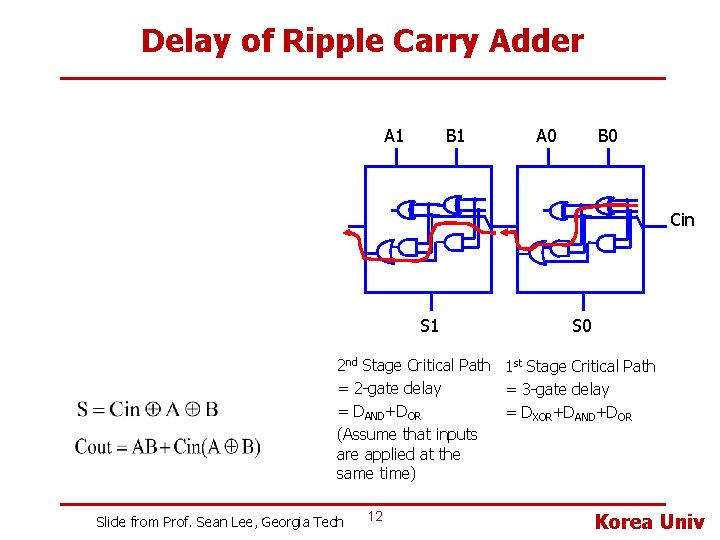
Delay of Ripple Carry Adder A 1 B 1 A 0 B 0 Cin S 1 S 0 2 nd Stage Critical Path 1 st Stage Critical Path = 2 -gate delay = 3 -gate delay = DAND+DOR = DXOR+DAND+DOR (Assume that inputs are applied at the same time) Slide from Prof. Sean Lee, Georgia Tech 12 Korea Univ

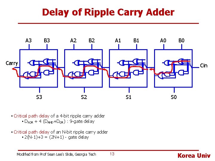
Delay of Ripple Carry Adder A 3 B 3 A 2 B 2 A 1 B 1 A 0 B 0 Carry Cin S 3 S 2 S 1 S 0 • Critical path delay of a 4 -bit ripple carry adder • DXOR + 4 (DAND+DOR) : 9 -gate delay • Critical path delay of an N-bit ripple carry adder • 2(N-1)+3 = (2 N+1) - gate delay Modified from Prof Sean Lee’s Slide, Georgia Tech 13 Korea Univ

Ripple-Carry Adder Delay • Ripple-carry adder has disadvantage of being slow when N is large § The delay of an N-bit ripple-carry adder is roughly tripple = N • t. FA (t. FA is the delay of a full adder) • A faster adder needs to address the serial propagation of the carry bit 14 Korea Univ

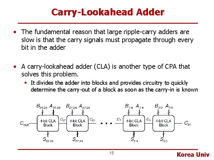
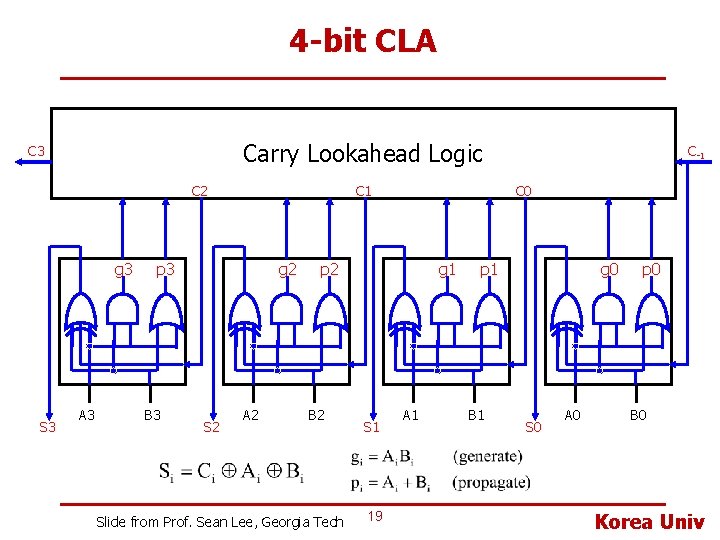
Carry-Lookahead Adder • The fundamental reason that large ripple-carry adders are slow is that the carry signals must propagate through every bit in the adder • A carry-lookahead adder (CLA) is another type of CPA that solves this problem. § It divides the adder into blocks and provides circuitry to quickly determine the carry-out of a block as soon as the carry-in is known 15 Korea Univ

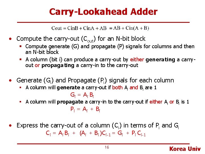
Carry-Lookahead Adder • Compute the carry-out (Cout) for an N-bit block § Compute generate (G) and propagate (P) signals for columns and then an N-bit block § A column (bit i) can produce a carry-out by either generating a carryout or propagating a carry-in to the carry-out • Generate (Gi) and Propagate (Pi) signals for each column § A column will generate a carry-out if both Ai and Bi are 1 G i = A i Bi § A column will propagate a carry-in to the carry-out if either Ai or Bi is 1 Pi = A i + B i • Express the carry-out of a column (Ci) in terms of Pi and Gi Ci = Ai Bi + (Ai + Bi )Ci-1 = Gi + Pi Ci-1 16 Korea Univ

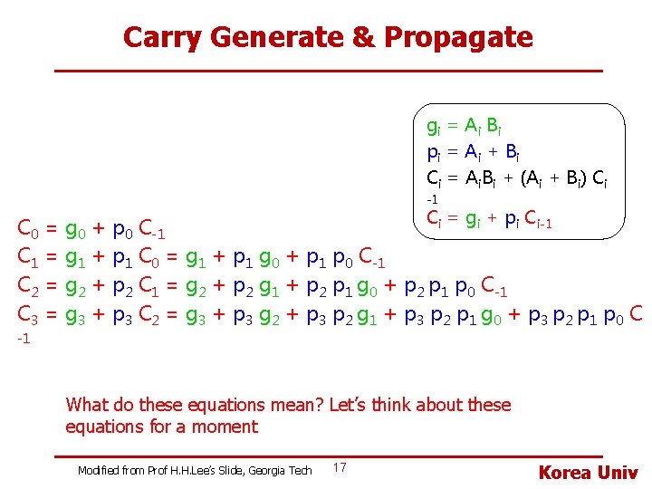
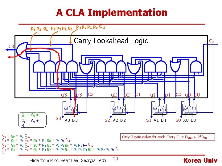
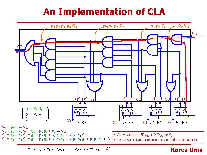
Carry Generate & Propagate gi = A i B i pi = A i + B i Ci = Ai. Bi + (Ai + Bi) Ci -1 C =g +p C i i-1 C 0 = g 0 + p 0 C-1 C 1 = g 1 + p 1 C 0 = g 1 + p 1 g 0 + p 1 p 0 C-1 C 2 = g 2 + p 2 C 1 = g 2 + p 2 g 1 + p 2 p 1 g 0 + p 2 p 1 p 0 C-1 C 3 = g 3 + p 3 C 2 = g 3 + p 3 g 2 + p 3 p 2 g 1 + p 3 p 2 p 1 g 0 + p 3 p 2 p 1 p 0 C -1 What do these equations mean? Let’s think about these equations for a moment Modified from Prof H. H. Lee’s Slide, Georgia Tech 17 Korea Univ

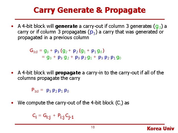
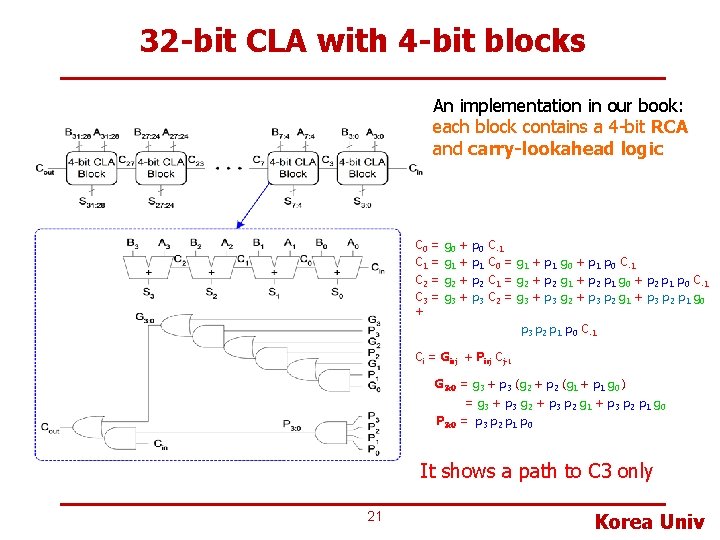
Carry Generate & Propagate • A 4 -bit block will generate a carry-out if column 3 generates (g 3) a carry or if column 3 propagates (p 3) a carry that was generated or propagated in a previous column G 3: 0 = g 3 + p 3 (g 2 + p 2 (g 1 + p 1 g 0 ) = g 3 + p 3 g 2 + p 3 p 2 g 1 + p 3 p 2 p 1 g 0 • A 4 -bit block will propagate a carry-in to the carry-out if all of the columns propagate the carry P 3: 0 = p 3 p 2 p 1 p 0 • We compute the carry-out of the 4 -bit block (Ci) as Ci = Gi: j + Pi: j Cj-1 18 Korea Univ

4 -bit CLA Carry Lookahead Logic C 3 C 2 g 3 S 3 A 3 C 1 p 3 B 3 g 2 S 2 A 2 C 0 p 2 B 2 Slide from Prof. Sean Lee, Georgia Tech g 1 S 1 19 C-1 A 1 p 1 B 1 g 0 S 0 A 0 p 0 B 0 Korea Univ

A CLA Implementation p 3 p 2 g 1 p 3 p 2 p 1 g 0 p 3 p 2 p 1 p 0 C-1 Carry Lookahead Logic C 3 gi = A i B i pi = A i + Bi p 3 S 3 A 3 B 3 g 2 C 2 p 2 S 2 A 2 B 2 C 0 = g 0 + p 0 C-1 C 1 = g 1 + p 1 C 0 = g 1 + p 1 g 0 + p 1 p 0 C-1 C 2 = g 2 + p 2 C 1 = g 2 + p 2 g 1 + p 2 p 1 g 0 + p 2 p 1 p 0 C-1 C 3 = g 3 + p 3 C 2 = g 3 + p 3 g 2 + p 3 p 2 g 1 + p 3 p 2 p 1 g 0 + p 3 p 2 p 1 p 0 C- C 1 C-1 g 1 p 1 S 1 A 1 B 1 C 0 g 0 p 0 S 0 A 0 B 0 Only 3 gate delay for each Carry C i = DAND + 2*DOR 1 Slide from Prof. Sean Lee, Georgia Tech 20 Korea Univ

32 -bit CLA with 4 -bit blocks An implementation in our book: each block contains a 4 -bit RCA and carry-lookahead logic C 0 = g 0 + p 0 C-1 C 1 = g 1 + p 1 C 0 = g 1 + p 1 g 0 + p 1 p 0 C-1 C 2 = g 2 + p 2 C 1 = g 2 + p 2 g 1 + p 2 p 1 g 0 + p 2 p 1 p 0 C-1 C 3 = g 3 + p 3 C 2 = g 3 + p 3 g 2 + p 3 p 2 g 1 + p 3 p 2 p 1 g 0 + p 3 p 2 p 1 p 0 C-1 Ci = Gi: j + Pi: j Cj-1 G 3: 0 = g 3 + p 3 (g 2 + p 2 (g 1 + p 1 g 0 ) = g 3 + p 3 g 2 + p 3 p 2 g 1 + p 3 p 2 p 1 g 0 P 3: 0 = p 3 p 2 p 1 p 0 It shows a path to C 3 only 21 Korea Univ

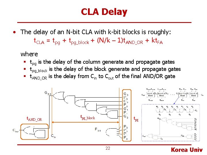
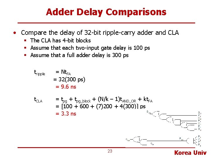
CLA Delay • The delay of an N-bit CLA with k-bit blocks is roughly: t. CLA = tpg + tpg_block + (N/k – 1)t. AND_OR + kt. FA where § tpg is the delay of the column generate and propagates § tpg_block is the delay of the block generate and propagates § t. AND_OR is the delay from Cin to Cout of the final AND/OR gate t. AND_OR tpg_block tpg 22 Korea Univ

Adder Delay Comparisons • Compare the delay of 32 -bit ripple-carry adder and CLA § The CLA has 4 -bit blocks § Assume that each two-input gate delay is 100 ps § Assume that a full adder delay is 300 ps tripple t. CLA = Nt. FA = 32(300 ps) = 9. 6 ns = tpg + tpg_block + (N/k – 1)t. AND_OR + kt. FA = [100 + 600 + (7)200 + 4(300)] ps = 3. 3 ns 23 Korea Univ
![VerilogHDL Representation module adder parameter N input N1 0 input output N1 0 Verilog-HDL Representation module adder #(parameter N = (input [N-1: 0] input output [N-1: 0]](https://slidetodoc.com/presentation_image_h/fc8b60684010c148f55315e9f3884dbb/image-24.jpg)
Verilog-HDL Representation module adder #(parameter N = (input [N-1: 0] input output [N-1: 0] output 8) a, b, cin, s, cout); assign {cout, s} = a + b + cin; endmodule 24 Korea Univ

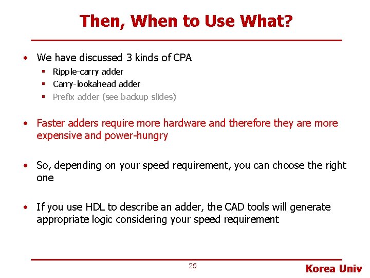
Then, When to Use What? • We have discussed 3 kinds of CPA § Ripple-carry adder § Carry-lookahead adder § Prefix adder (see backup slides) • Faster adders require more hardware and therefore they are more expensive and power-hungry • So, depending on your speed requirement, you can choose the right one • If you use HDL to describe an adder, the CAD tools will generate appropriate logic considering your speed requirement 25 Korea Univ

Backup Slides 26 Korea Univ

An Implementation of CLA p 3 p 2 p 1 p 0 C-1 p 0 C-1 C 3 g 3 p 3 C 2 gi = A i B i pi = A i + Bi g 2 p 2 C 1 S 3 A 3 B 3 C 0 = g 0 + p 0 C-1 C 1 = g 1 + p 1 C 0 = g 1 + p 1 g 0 + p 1 p 0 C-1 C 2 = g 2 + p 2 C 1 = g 2 + p 2 g 1 + p 2 p 1 g 0 + p 2 p 1 p 0 C-1 C 3 = g 3 + p 3 C 2 = g 3 + p 3 g 2 + p 3 p 2 g 1 + p 3 p 2 p 1 g 0 + p 3 p 2 p 1 p 0 C 1 Slide from Prof. Sean Lee, Georgia Tech 27 S 2 A 2 B 2 g 1 p 1 C 0 S 1 A 1 B 1 g 0 p 0 S 0 A 0 B 0 § Carry delay is 4*DAND + 2*DOR for C 3 § Reuse some gate output results in little improvement Korea Univ

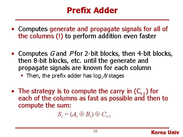
Prefix Adder • Computes generate and propagate signals for all of the columns (!) to perform addition even faster • Computes G and P for 2 -bit blocks, then 4 -bit blocks, then 8 -bit blocks, etc. until the generate and propagate signals are known for each column § Then, the prefix adder has log 2 N stages • The strategy is to compute the carry in (Ci-1) for each of the columns as fast as possible and then to compute the sum: Si = (Ai Å Bi) Å Ci-1 28 Korea Univ

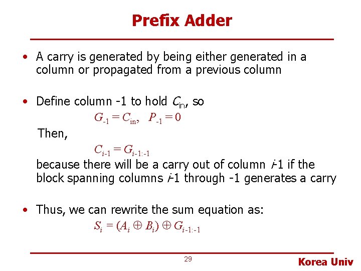
Prefix Adder • A carry is generated by being either generated in a column or propagated from a previous column • Define column -1 to hold Cin, so G-1 = Cin, P-1 = 0 Then, Ci-1 = Gi-1: -1 because there will be a carry out of column i-1 if the block spanning columns i-1 through -1 generates a carry • Thus, we can rewrite the sum equation as: Si = (Ai Å Bi) Å Gi-1: -1 29 Korea Univ

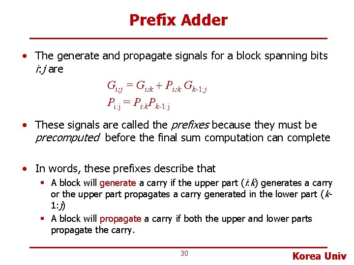
Prefix Adder • The generate and propagate signals for a block spanning bits i: j are Gi: j = Gi: k + Pi: k Gk-1: j Pi: j = Pi: k. Pk-1: j • These signals are called the prefixes because they must be precomputed before the final sum computation can complete • In words, these prefixes describe that § A block will generate a carry if the upper part (i: k) generates a carry or the upper part propagates a carry generated in the lower part ( k 1: j) § A block will propagate a carry if both the upper and lower parts propagate the carry. 30 Korea Univ

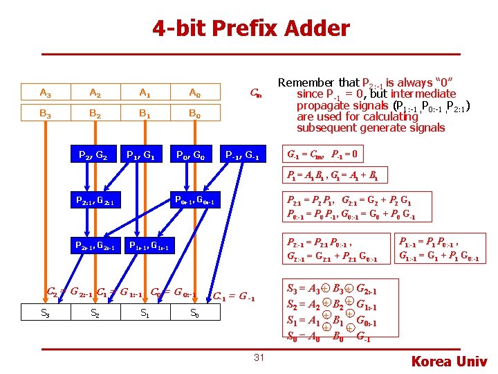
4 -bit Prefix Adder A 3 A 2 A 1 A 0 B 3 B 2 B 1 B 0 P 2, G 2 P 1, G 1 Cin P 0, G 0 P-1, G-1 Remember that P 2: -1 is always “ 0” since P-1 = 0, but intermediate propagate signals (P 1: -1 , P 0: -1 , P 2: 1) are used for calculating subsequent generate signals G-1 = Cin, P-1 = 0 P i = A i B i , Gi = A i + B i P 2: 1, G 2: 1 P 2: -1, G 2: -1 P 0: -1, G 0: -1 P 2: -1 = P 2: 1 P 0: -1 , G 2: -1 = G 2: 1 + P 2: 1 G 0: -1 P 1: -1, G 1: -1 C 2 = G 2: -1 C 1 = G 1: -1 C 0 = G 0: -1 S 3 S 2 P 2: 1 = P 2 P 1, G 2: 1 = G 2 + P 2 G 1 P 0: -1 = P 0 P-1, G 0: -1 = G 0 + P 0 G-1 S 1 C-1 = G -1 S 0 31 P 1: -1 = P 1 P 0: -1 , G 1: -1 = G 1 + P 1 G 0: -1 S 3 = A 3 + B 3 + G 2: -1 S 2 = A 2 + B 2 + G 1: -1 + S 1 = A 1 + B 1 G 0: -1 + + S 0 = A 0 B 0 G-1 Korea Univ

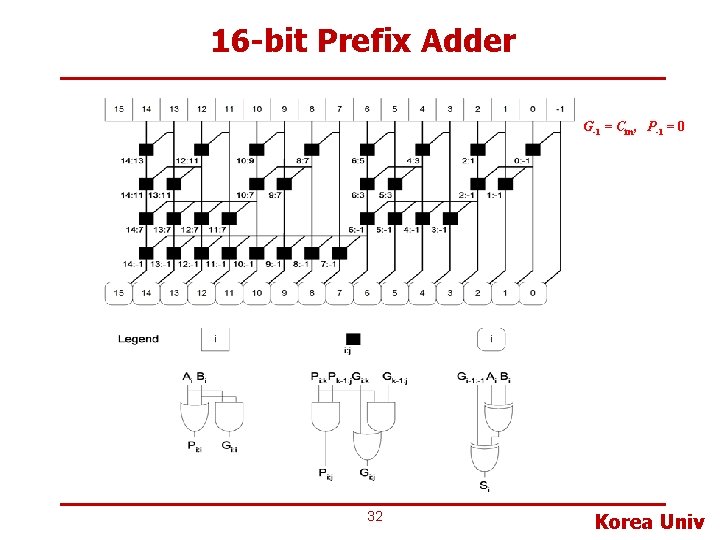
16 -bit Prefix Adder G-1 = Cin, P-1 = 0 32 Korea Univ

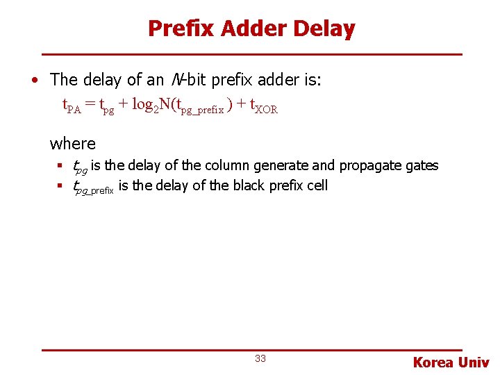
Prefix Adder Delay • The delay of an N-bit prefix adder is: t. PA = tpg + log 2 N(tpg_prefix ) + t. XOR where § tpg is the delay of the column generate and propagates § tpg_prefix is the delay of the black prefix cell 33 Korea Univ