COSC 3 P 92 Cosc 3 P 92

- Slides: 52

COSC 3 P 92 Cosc 3 P 92 Week 2 Lecture slides The very first law in advertising is to avoid the concrete promise and cultivate the delightfully vague. Bill Cosby (1937 - ) 1

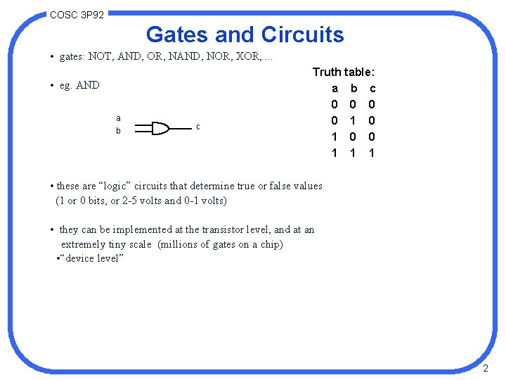
COSC 3 P 92 Gates and Circuits • gates: NOT, AND, OR, NAND, NOR, XOR, . . . • eg. AND a b c Truth table: a b c 0 0 1 1 1 • these are “logic” circuits that determine true or false values (1 or 0 bits, or 2 -5 volts and 0 -1 volts) • they can be implemented at the transistor level, and at an extremely tiny scale (millions of gates on a chip) • “device level” 2

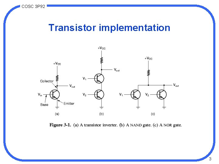
COSC 3 P 92 Transistor implementation 3

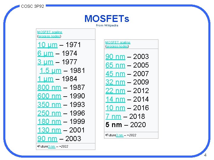
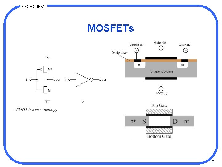
COSC 3 P 92 MOSFETs From Wikipedia MOSFET scaling (process nodes) 10 µm – 1971 6 µm – 1974 3 µm – 1977 1. 5 µm – 1981 1 µm – 1984 800 nm – 1987 600 nm – 1990 350 nm – 1993 250 nm – 1996 180 nm – 1999 130 nm – 2001 90 nm – 2003 MOSFET scaling (process nodes) 90 nm – 2003 65 nm – 2005 45 nm – 2007 32 nm – 2009 22 nm – 2012 14 nm – 2014 10 nm – 2016 7 nm – 2018 5 nm – 2020 • Future 3 nm – ~2022 4

COSC 3 P 92 MOSFETs 5

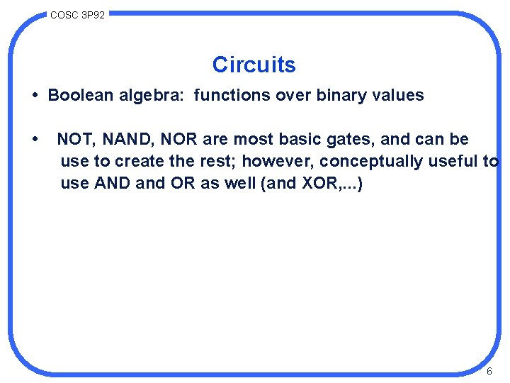
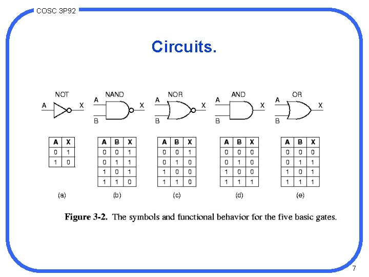
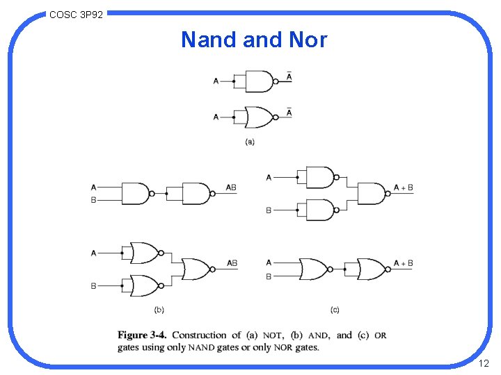
COSC 3 P 92 Circuits • Boolean algebra: functions over binary values • NOT, NAND, NOR are most basic gates, and can be use to create the rest; however, conceptually useful to use AND and OR as well (and XOR, . . . ) 6

COSC 3 P 92 Circuits. 7

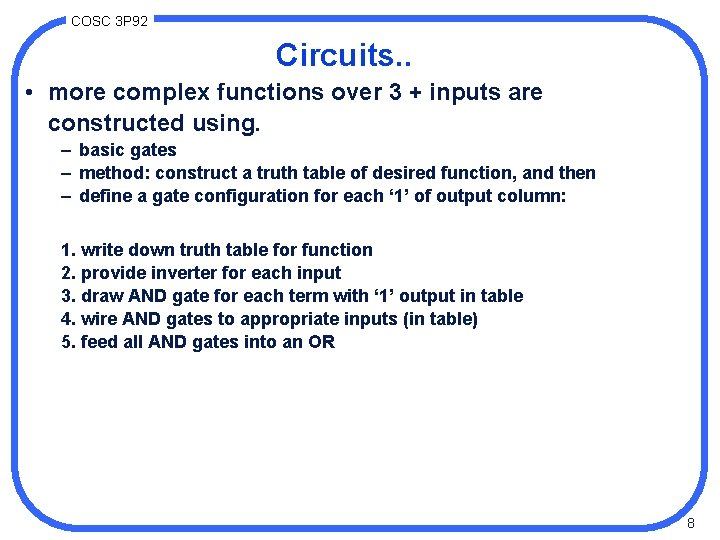
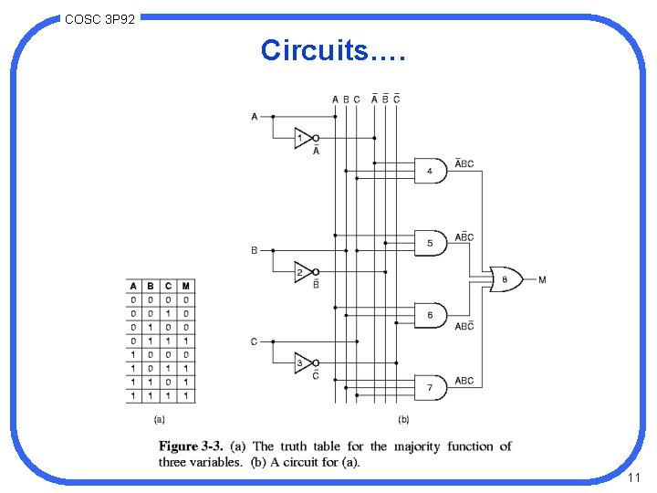
COSC 3 P 92 Circuits. . • more complex functions over 3 + inputs are constructed using. – basic gates – method: construct a truth table of desired function, and then – define a gate configuration for each ‘ 1’ of output column: 1. write down truth table for function 2. provide inverter for each input 3. draw AND gate for each term with ‘ 1’ output in table 4. wire AND gates to appropriate inputs (in table) 5. feed all AND gates into an OR 8

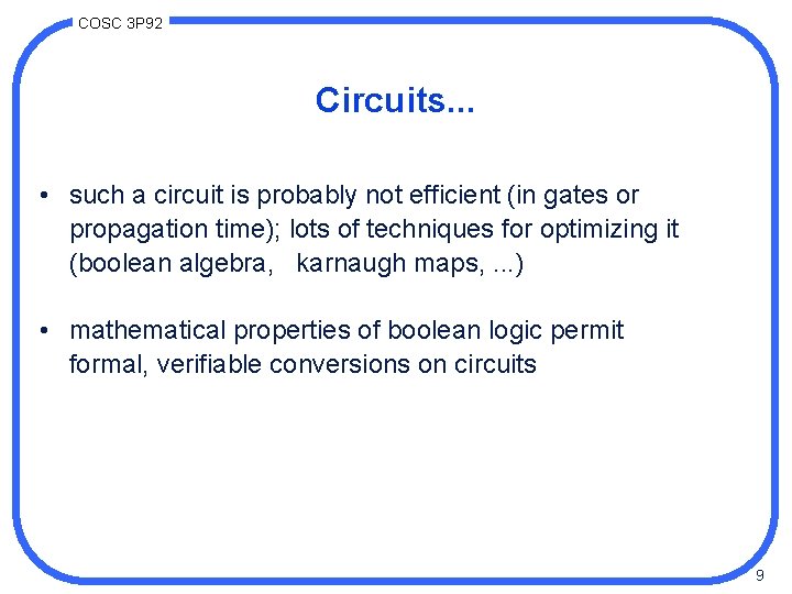
COSC 3 P 92 Circuits. . . • such a circuit is probably not efficient (in gates or propagation time); lots of techniques for optimizing it (boolean algebra, karnaugh maps, . . . ) • mathematical properties of boolean logic permit formal, verifiable conversions on circuits 9

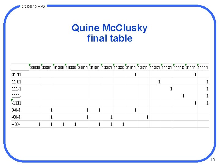
COSC 3 P 92 Quine Mc. Clusky final table 10

COSC 3 P 92 Circuits…. 11

COSC 3 P 92 Nand Nor 12

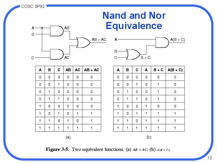
COSC 3 P 92 Nand Nor Equivalence 13

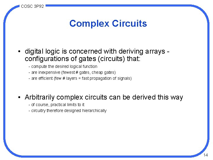
COSC 3 P 92 Complex Circuits • digital logic is concerned with deriving arrays - configurations of gates (circuits) that: - compute the desired logical function - are inexpensive (fewest # gates, cheap gates) - are efficient (few # layers = fast propagation of signals) • Arbitrarily complex circuits can be derived this way - of course, practical limits to it - circuitry therefore designed hierarchically 14

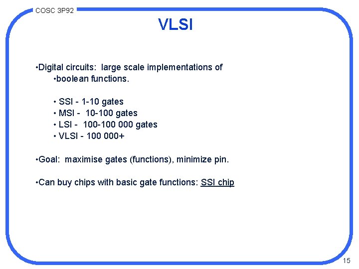
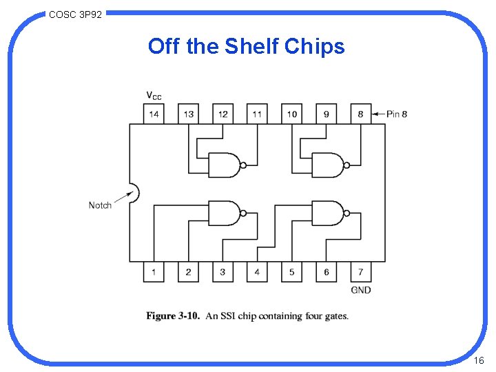
COSC 3 P 92 VLSI • Digital circuits: large scale implementations of • boolean functions. • SSI - 1 -10 gates • MSI - 10 -100 gates • LSI - 100 -100 000 gates • VLSI - 100 000+ • Goal: maximise gates (functions), minimize pin. • Can buy chips with basic gate functions: SSI chip 15

COSC 3 P 92 Off the Shelf Chips 16

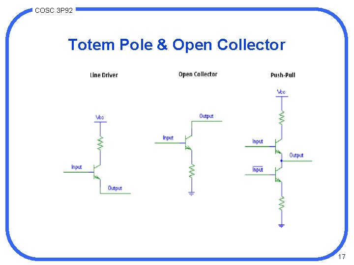
COSC 3 P 92 Totem Pole & Open Collector 17

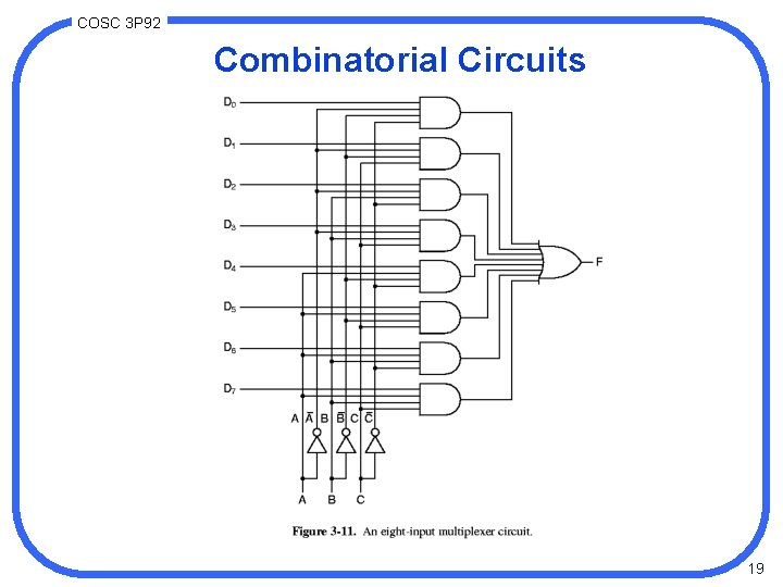
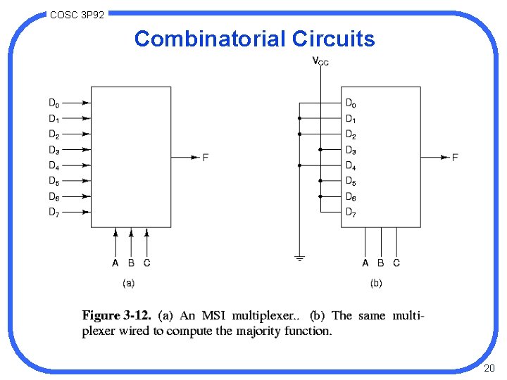
COSC 3 P 92 Combinatorial Circuits • combinatorial circuits: outputs dependent upon input values • One convenient technique: provide general circuits that permit user definition of function: MSI chips • eg. multiplexer: 2^n data inputs, n control lines, 1 output – each AND gate toggled by different combination of control; value specified by data input 18

COSC 3 P 92 Combinatorial Circuits 19

COSC 3 P 92 Combinatorial Circuits 20

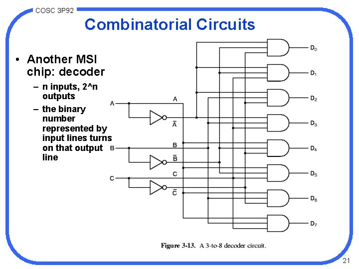
COSC 3 P 92 Combinatorial Circuits • Another MSI chip: decoder – n inputs, 2^n outputs – the binary number represented by input lines turns on that output line 21

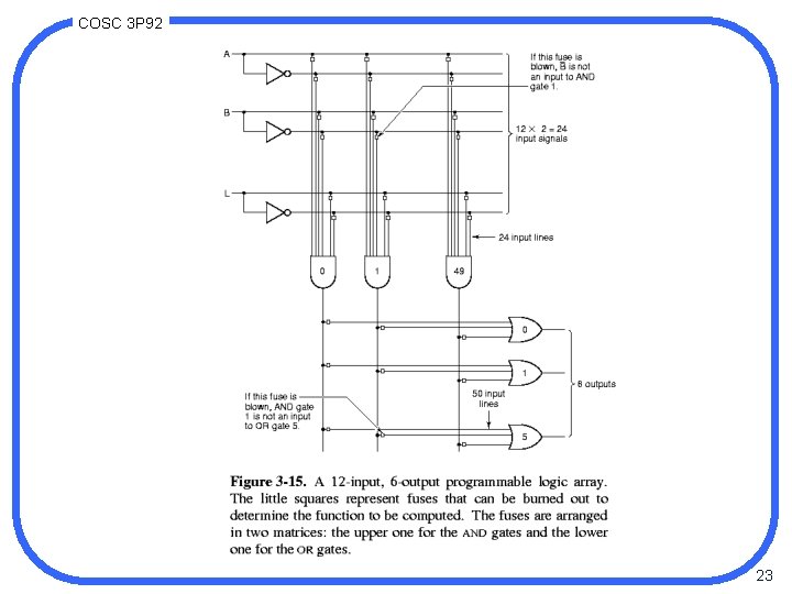
COSC 3 P 92 Combinatorial Circuits • Yet another MSI: Programmed Logic Array (PLA) – using truth table, user burns connections on this circuit, which effectively matches input data line patterns to appropriate output line patterns • possible to rewrite some PLA circuits; cheaper to mass-produce write-once ones. 22

COSC 3 P 92 23

COSC 3 P 92 Eprom 24

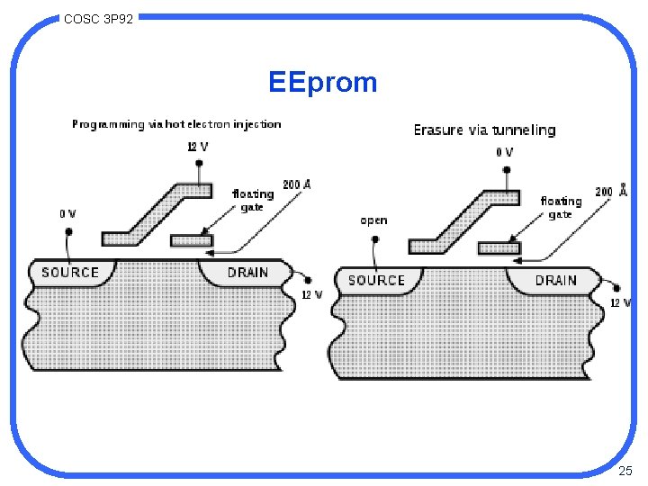
COSC 3 P 92 EEprom 25

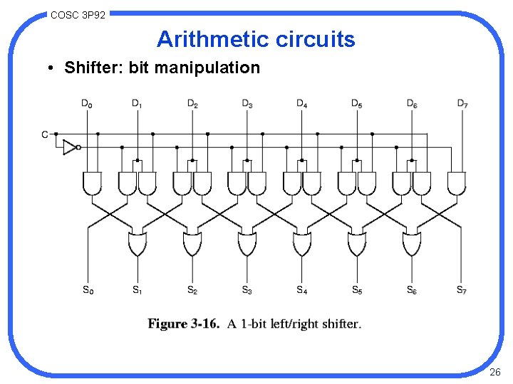
COSC 3 P 92 Arithmetic circuits • Shifter: bit manipulation 26

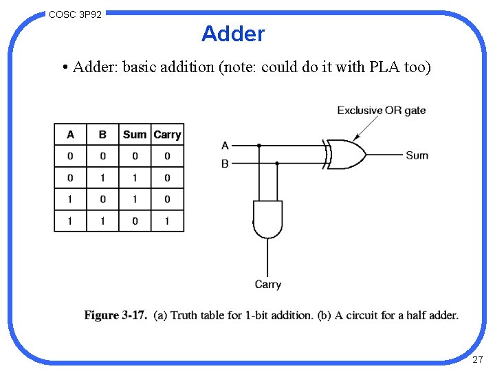
COSC 3 P 92 Adder • Adder: basic addition (note: could do it with PLA too) 27

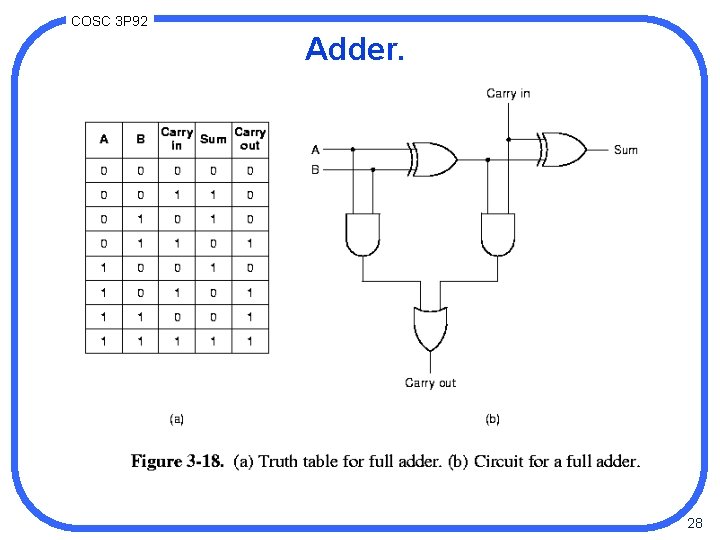
COSC 3 P 92 Adder. 28

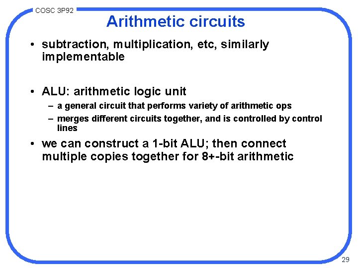
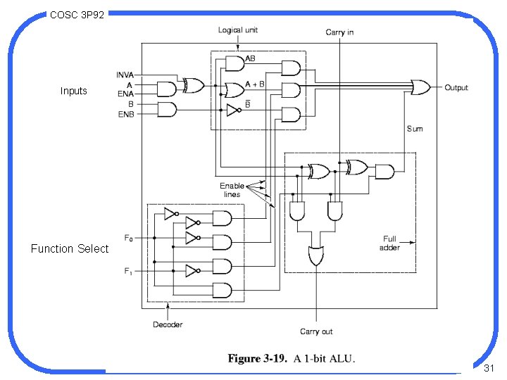
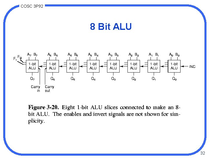
COSC 3 P 92 Arithmetic circuits • subtraction, multiplication, etc, similarly implementable • ALU: arithmetic logic unit – a general circuit that performs variety of arithmetic ops – merges different circuits together, and is controlled by control lines • we can construct a 1 -bit ALU; then connect multiple copies together for 8+-bit arithmetic 29

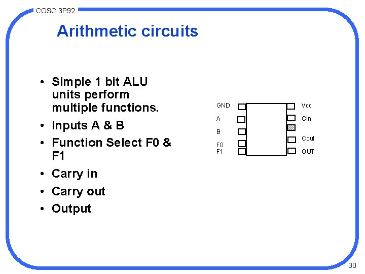
COSC 3 P 92 Arithmetic circuits • Simple 1 bit ALU units perform multiple functions. • Inputs A & B • Function Select F 0 & F 1 • Carry in • Carry out • Output GND Vcc A Cin B F 0 F 1 Cout OUT 30

COSC 3 P 92 Inputs Function Select 31

COSC 3 P 92 8 Bit ALU 32

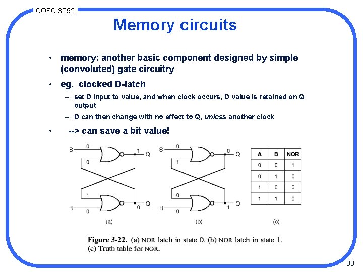
COSC 3 P 92 Memory circuits • memory: another basic component designed by simple (convoluted) gate circuitry • eg. clocked D-latch – set D input to value, and when clock occurs, D value is retained on Q output – D can then change with no effect to Q, unless another clock • --> can save a bit value! 33

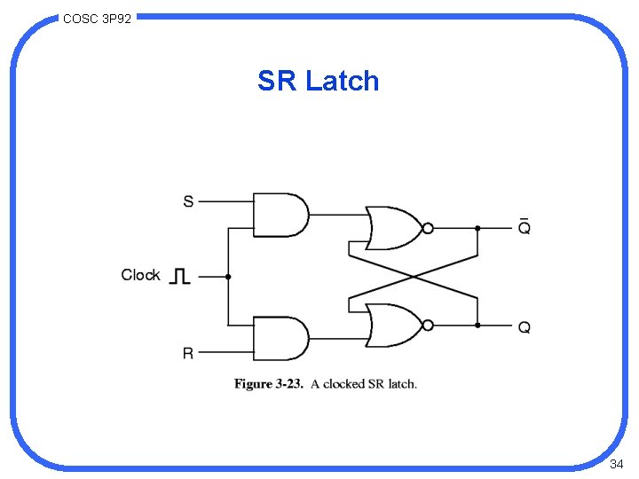
COSC 3 P 92 SR Latch 34

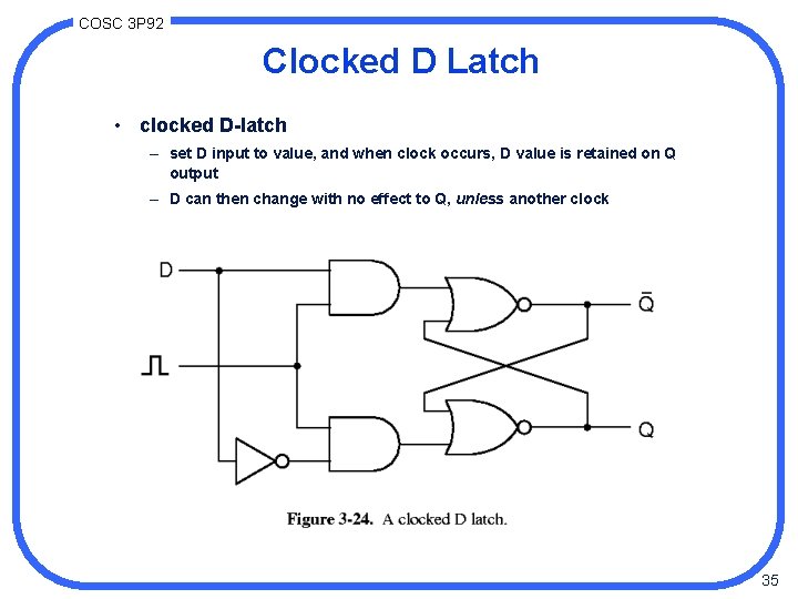
COSC 3 P 92 Clocked D Latch • clocked D-latch – set D input to value, and when clock occurs, D value is retained on Q output – D can then change with no effect to Q, unless another clock 35

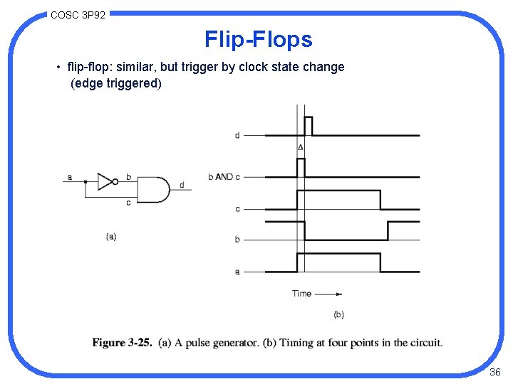
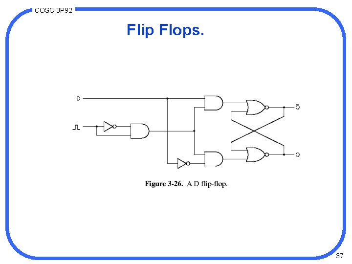
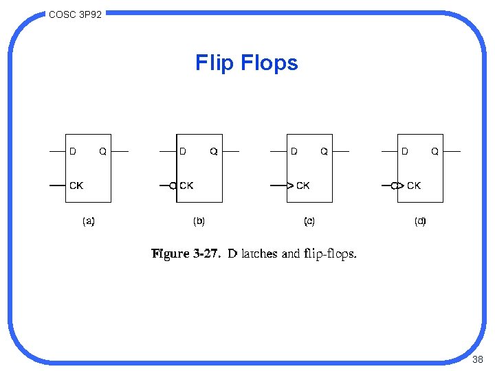
COSC 3 P 92 Flip-Flops • flip-flop: similar, but trigger by clock state change (edge triggered) 36

COSC 3 P 92 Flip Flops. 37

COSC 3 P 92 Flip Flops 38

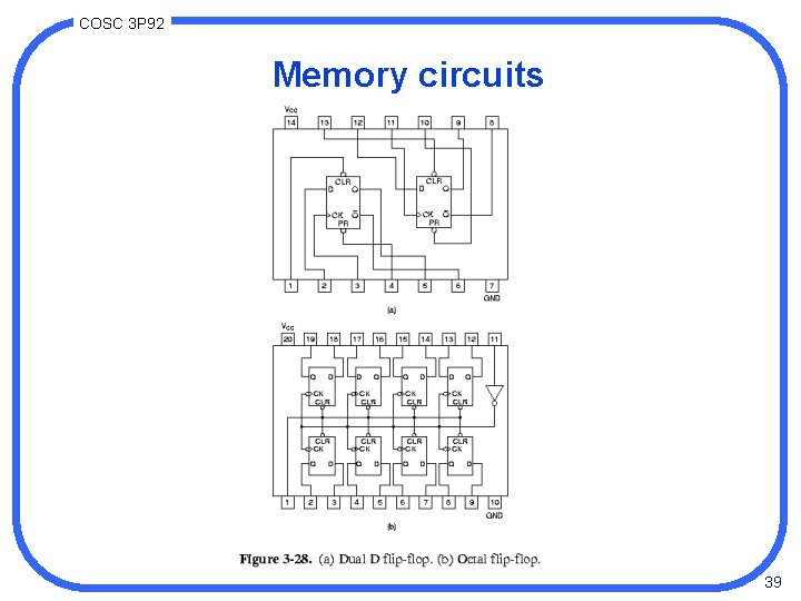
COSC 3 P 92 Memory circuits 39

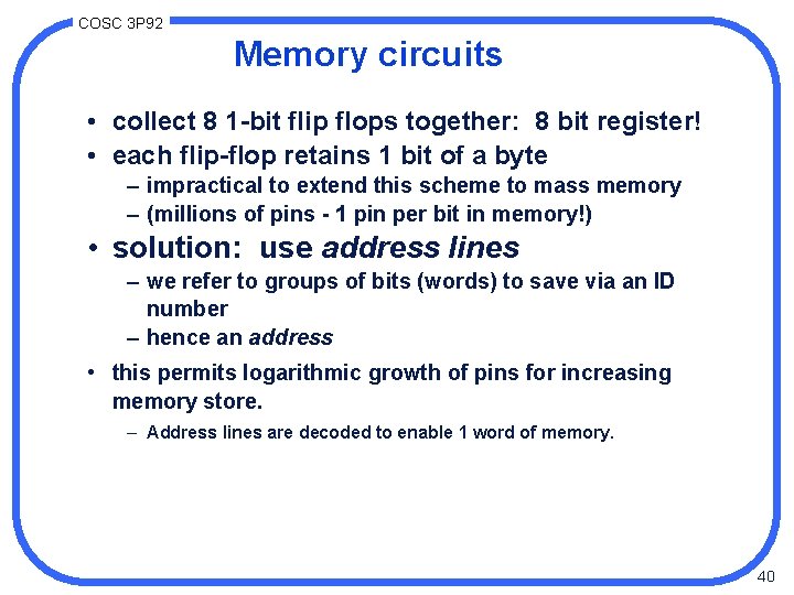
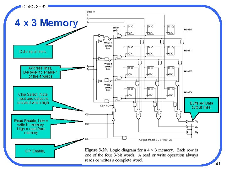
COSC 3 P 92 Memory circuits • collect 8 1 -bit flip flops together: 8 bit register! • each flip-flop retains 1 bit of a byte – impractical to extend this scheme to mass memory – (millions of pins - 1 pin per bit in memory!) • solution: use address lines – we refer to groups of bits (words) to save via an ID number – hence an address • this permits logarithmic growth of pins for increasing memory store. – Address lines are decoded to enable 1 word of memory. 40

COSC 3 P 92 4 x 3 Memory Data input lines, Address lines, Decoded to enable 1 of the 4 words Chip Select, Note Input and output is enabled when high Buffered Data output lines, Read Enable, Low = write to memory. High = read from memory O/P Enable, 41

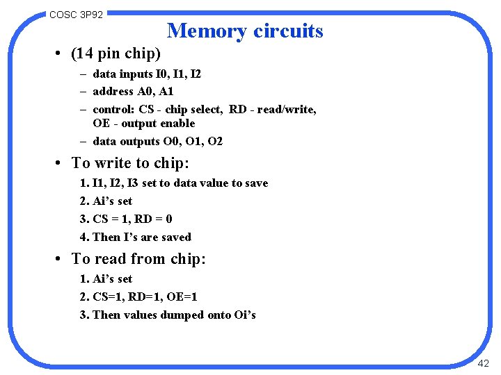
COSC 3 P 92 Memory circuits • (14 pin chip) – data inputs I 0, I 1, I 2 – address A 0, A 1 – control: CS - chip select, RD - read/write, OE - output enable – data outputs O 0, O 1, O 2 • To write to chip: 1. I 1, I 2, I 3 set to data value to save 2. Ai’s set 3. CS = 1, RD = 0 4. Then I’s are saved • To read from chip: 1. Ai’s set 2. CS=1, RD=1, OE=1 3. Then values dumped onto Oi’s 42

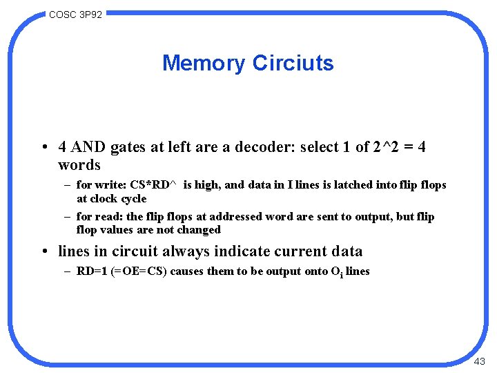
COSC 3 P 92 Memory Circiuts • 4 AND gates at left are a decoder: select 1 of 2^2 = 4 words – for write: CS*RD^ is high, and data in I lines is latched into flip flops at clock cycle – for read: the flip flops at addressed word are sent to output, but flip flop values are not changed • lines in circuit always indicate current data – RD=1 (=OE=CS) causes them to be output onto Oi lines 43

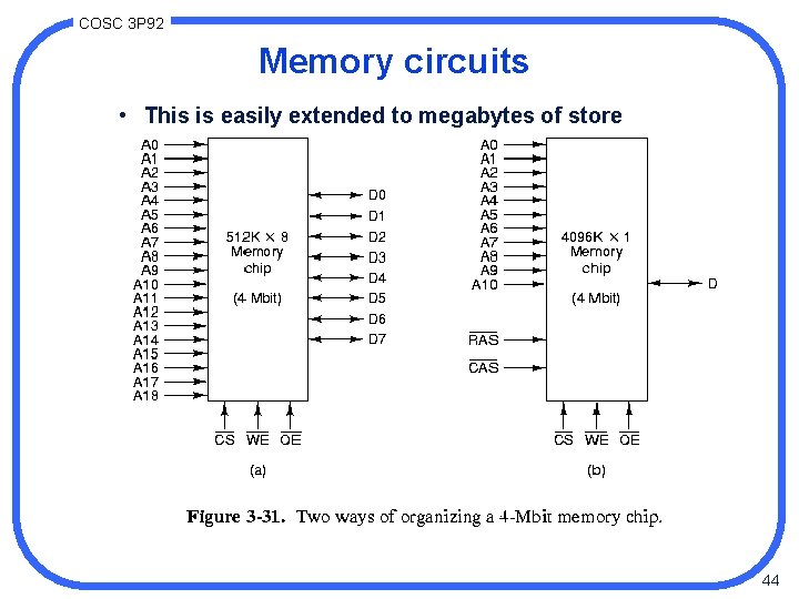
COSC 3 P 92 Memory circuits • This is easily extended to megabytes of store 44

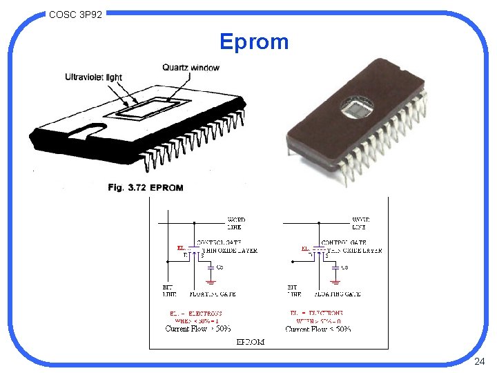
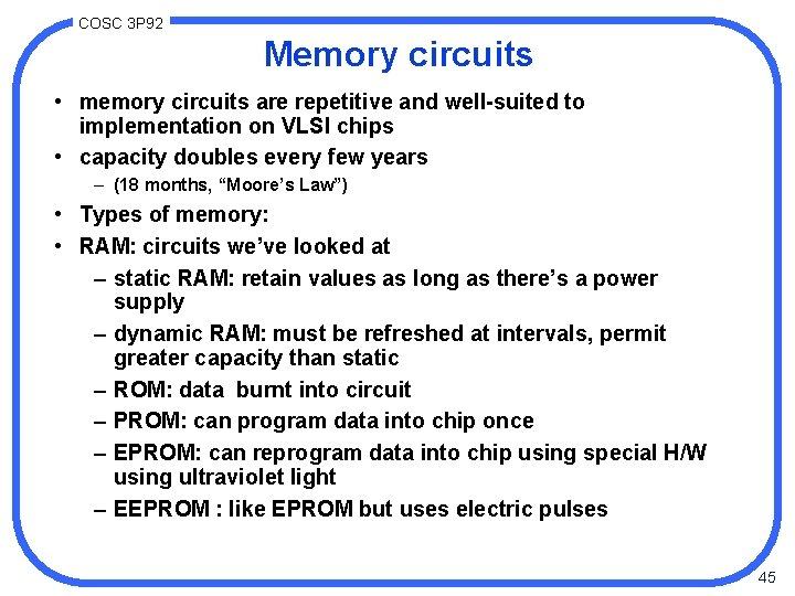
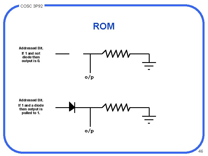
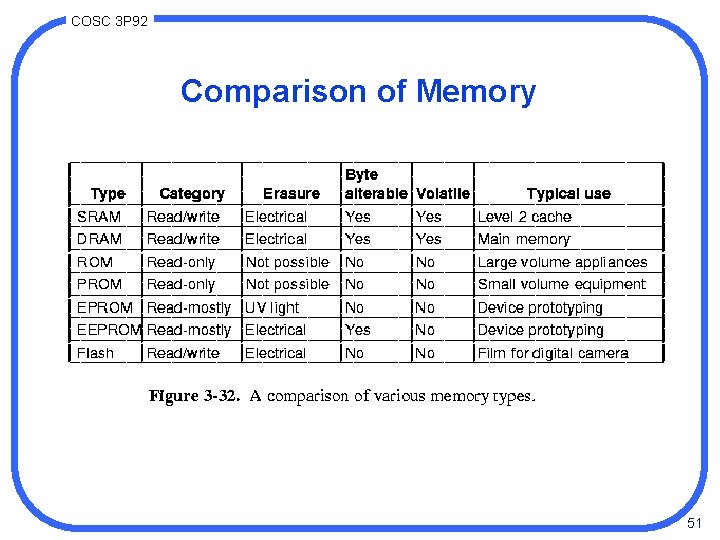
COSC 3 P 92 Memory circuits • memory circuits are repetitive and well-suited to implementation on VLSI chips • capacity doubles every few years – (18 months, “Moore’s Law”) • Types of memory: • RAM: circuits we’ve looked at – static RAM: retain values as long as there’s a power supply – dynamic RAM: must be refreshed at intervals, permit greater capacity than static – ROM: data burnt into circuit – PROM: can program data into chip once – EPROM: can reprogram data into chip using special H/W using ultraviolet light – EEPROM : like EPROM but uses electric pulses 45

COSC 3 P 92 ROM Addressed Bit. If 1 and not diode then output is 0. o/p Addressed Bit. If 1 and a diode then output is pulled to 1. o/p 46

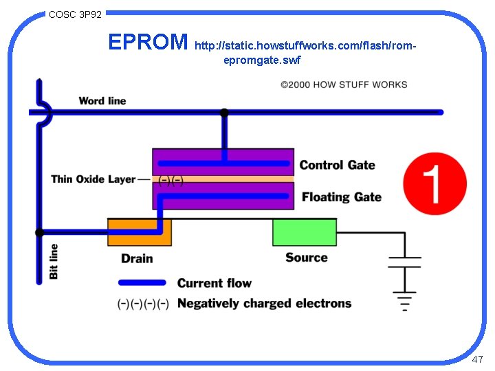
COSC 3 P 92 EPROM http: //static. howstuffworks. com/flash/romepromgate. swf 47

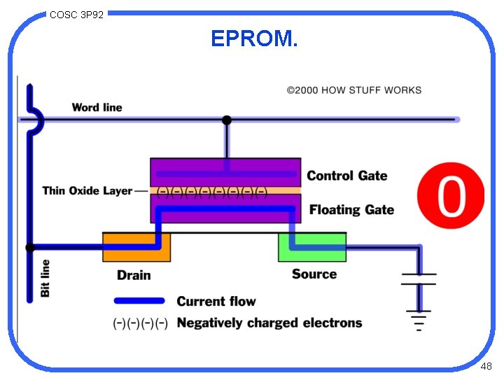
COSC 3 P 92 EPROM. 48

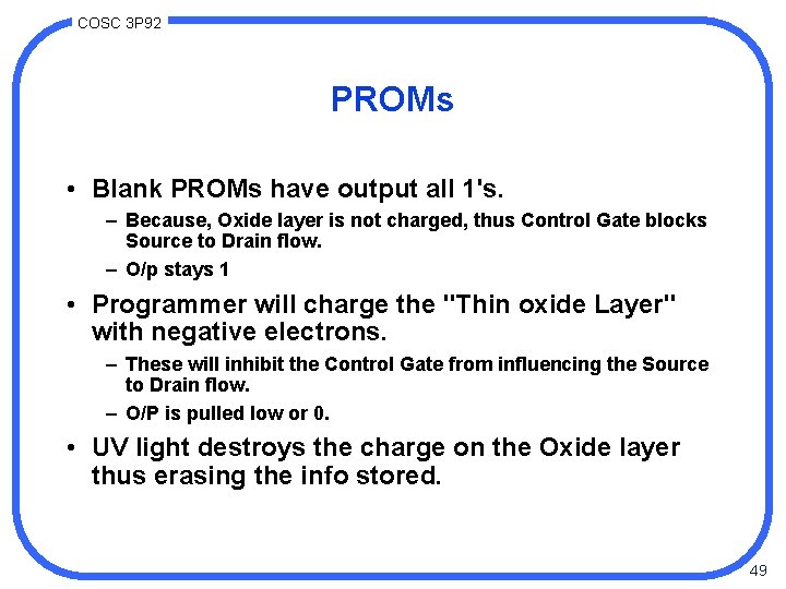
COSC 3 P 92 PROMs • Blank PROMs have output all 1's. – Because, Oxide layer is not charged, thus Control Gate blocks Source to Drain flow. – O/p stays 1 • Programmer will charge the "Thin oxide Layer" with negative electrons. – These will inhibit the Control Gate from influencing the Source to Drain flow. – O/P is pulled low or 0. • UV light destroys the charge on the Oxide layer thus erasing the info stored. 49

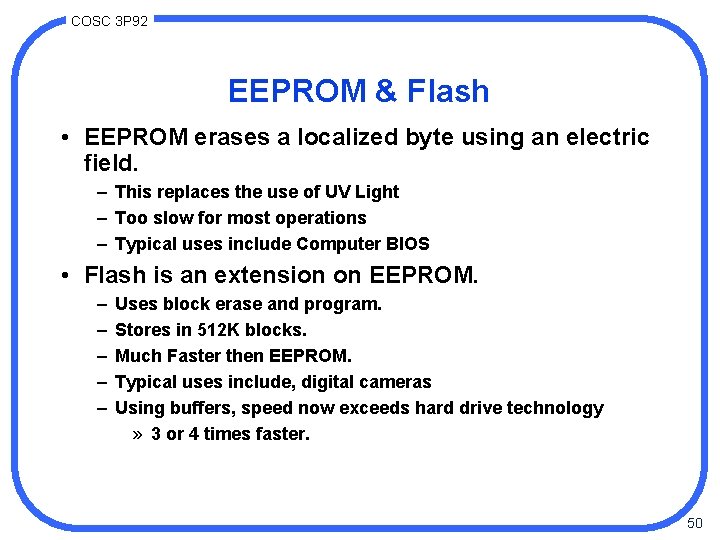
COSC 3 P 92 EEPROM & Flash • EEPROM erases a localized byte using an electric field. – This replaces the use of UV Light – Too slow for most operations – Typical uses include Computer BIOS • Flash is an extension on EEPROM. – – – Uses block erase and program. Stores in 512 K blocks. Much Faster then EEPROM. Typical uses include, digital cameras Using buffers, speed now exceeds hard drive technology » 3 or 4 times faster. 50

COSC 3 P 92 Comparison of Memory 51

COSC 3 P 92 The end 52