Contents Preliminaries Analog vs Digital Basic Gates Verilog
Contents • Preliminaries • Analog vs. Digital • Basic Gates • Verilog (Part I) History of Hardware Description Language (HLD)s HDL Abstraction Verilog Constructs (Data Types, Modules, Operators) Modeling Concurrent Functionality in Verilog (Logical, Conditional, and Delay Assignments) • Structural Design and Hierarchy (Lower-Level Module Instantiation, Gate Level Primitives, User-Defined Primitives) • • • Verilog (Part II) • Procedural Assignment (Procedural Blocks and Assignments, Statement Groups, Local Variables) • Conditional Programming Construct (if-else, casez, casex, and Loops) • Behavioral Modeling • RTL Modeling 1

Verilog Concepts 2
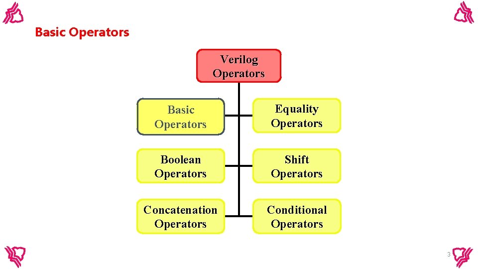
Basic Operators Verilog Operators Basic Operators Equality Operators Boolean Operators Shift Operators Concatenation Operators Conditional Operators 3
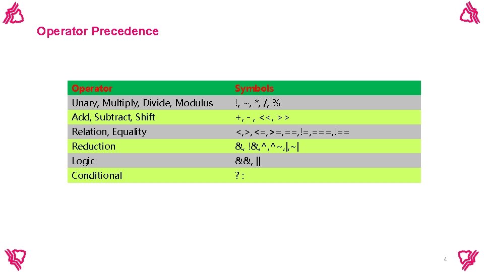
Operator Precedence Operator Symbols Unary, Multiply, Divide, Modulus !, ~, *, /, % Add, Subtract, Shift +, - , <<, >> Relation, Equality <, >, <=, >=, ==, !=, ===, !== Reduction &, !&, ^, ^~, |, ~| Logic &&, || Conditional ? : 4
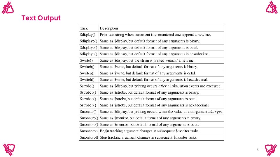
Text Output 5
Verilog HDL Abstraction Levels • Behavioral Models : Higher level of modeling where behavior of logic is modeled. • RTL Models : Logic is modeled at register level. • Structural Models : Logic is modeled at both register level and gate level. • Switch (Transistor) Models: Logic is modeled Transistor level. 6
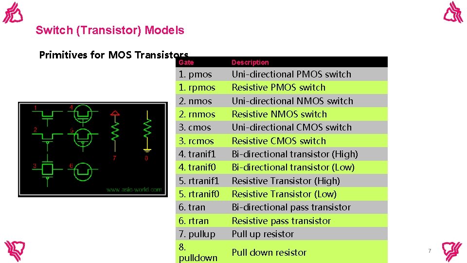
Switch (Transistor) Models Primitives for MOS Transistors Gate Description 1. pmos Uni-directional PMOS switch 1. rpmos Resistive PMOS switch 2. nmos Uni-directional NMOS switch 2. rnmos Resistive NMOS switch 3. cmos Uni-directional CMOS switch 3. rcmos Resistive CMOS switch 4. tranif 1 Bi-directional transistor (High) 4. tranif 0 Bi-directional transistor (Low) 5. rtranif 1 Resistive Transistor (High) 5. rtranif 0 Resistive Transistor (Low) 6. tran Bi-directional pass transistor 6. rtran Resistive pass transistor 7. pullup Pull up resistor 8. pulldown Pull down resistor 7
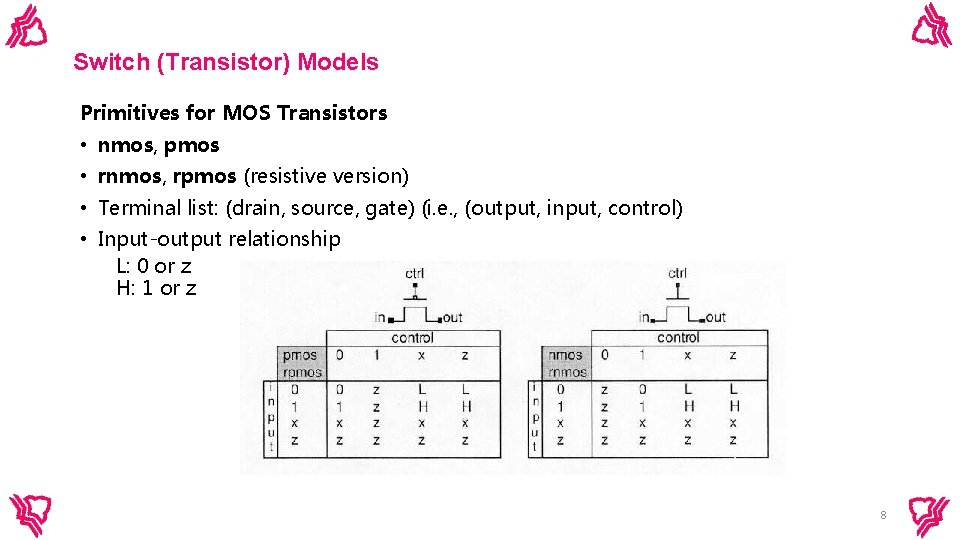
Switch (Transistor) Models Primitives for MOS Transistors • nmos, pmos • rnmos, rpmos (resistive version) • Terminal list: (drain, source, gate) (i. e. , (output, input, control) • Input-output relationship L: 0 or z H: 1 or z 8
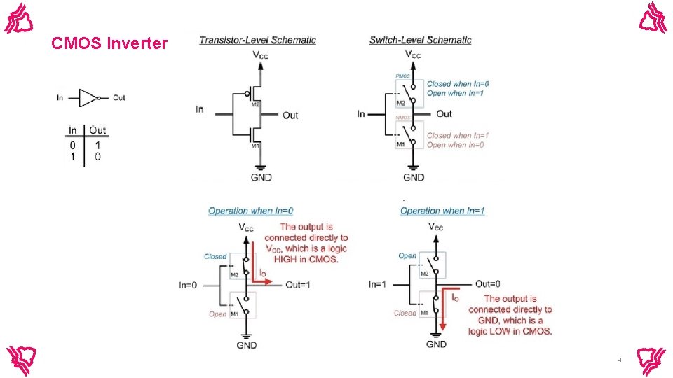
CMOS Inverter 9
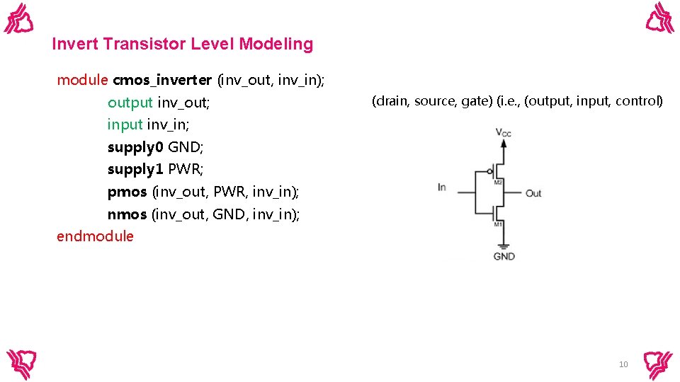
Invert Transistor Level Modeling module cmos_inverter (inv_out, inv_in); output inv_out; (drain, source, gate) (i. e. , (output, input, control) input inv_in; supply 0 GND; supply 1 PWR; pmos (inv_out, PWR, inv_in); nmos (inv_out, GND, inv_in); endmodule 10
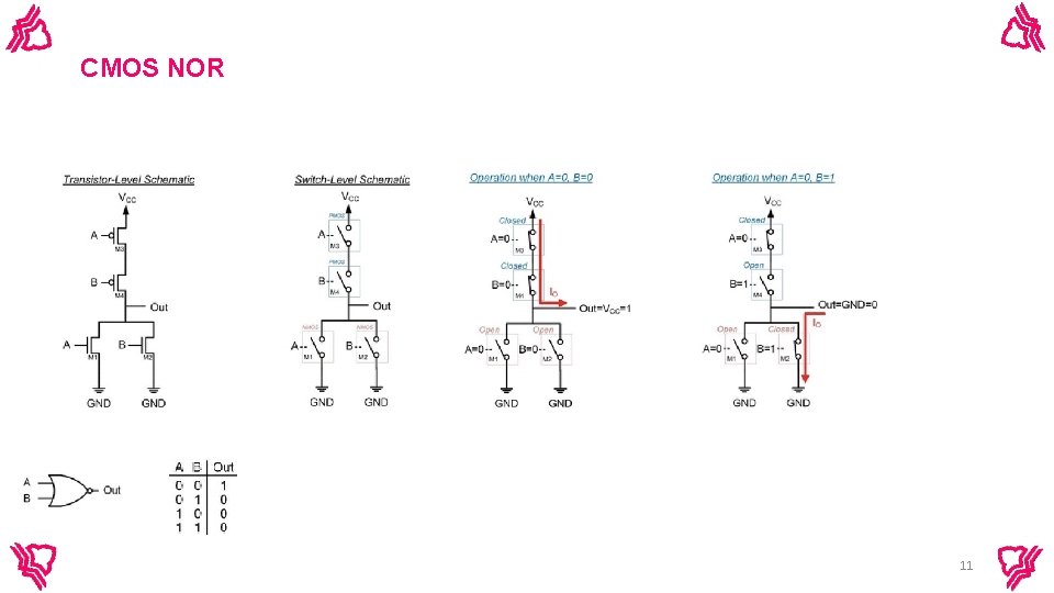
CMOS NOR 11
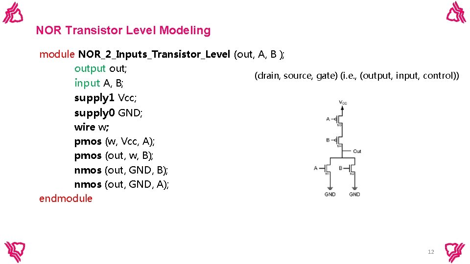
NOR Transistor Level Modeling module NOR_2_Inputs_Transistor_Level (out, A, B ); output out; (drain, source, gate) (i. e. , (output, input, control)) input A, B; supply 1 Vcc; supply 0 GND; wire w; pmos (w, Vcc, A); pmos (out, w, B); nmos (out, GND, A); endmodule 12
Gate Level Modeling • In gate level, basic gates are used as primitives and used as such to perform the corresponding operation. • We represent hardware circuits from basic logic gates. • Verilog supports primitive gates to facilitate this level. • We see only netlist (gates and wires) in the code of Gate Level modeling. 13
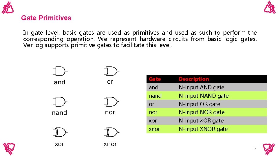
Gate Primitives In gate level, basic gates are used as primitives and used as such to perform the corresponding operation. We represent hardware circuits from basic logic gates. Verilog supports primitive gates to facilitate this level. Gate Description and N-input AND gate nand N-input NAND gate or N-input OR gate nor N-input NOR gate xor N-input XOR gate xnor N-input XNOR gate 14
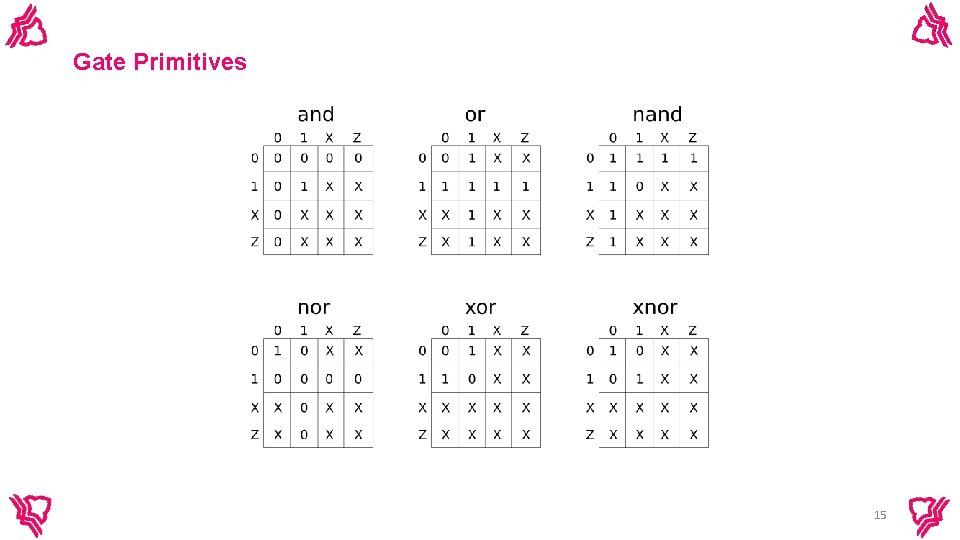
Gate Primitives 15
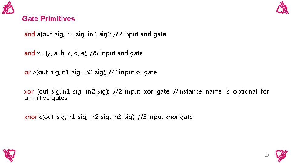
Gate Primitives and a(out_sig, in 1_sig, in 2_sig); //2 input and gate and x 1 (y, a, b, c, d, e); //5 input and gate or b(out_sig, in 1_sig, in 2_sig); //2 input or gate xor (out_sig, in 1_sig, in 2_sig); //2 input xor gate //instance name is optional for primitive gates xnor c(out_sig, in 1_sig, in 2_sig, in 3_sig); //3 input xnor gate 16
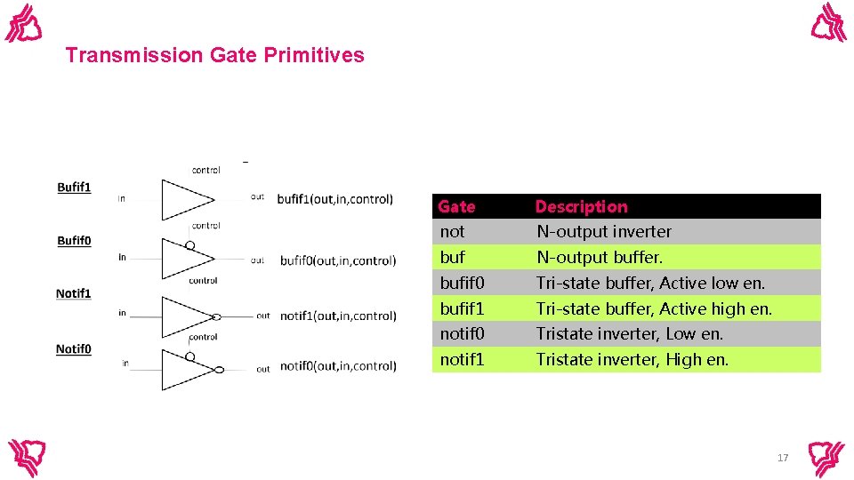
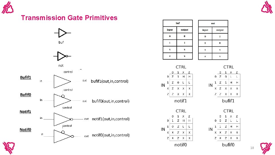
Transmission Gate Primitives Gate Description not N-output inverter buf N-output buffer. bufif 0 Tri-state buffer, Active low en. bufif 1 Tri-state buffer, Active high en. notif 0 Tristate inverter, Low en. notif 1 Tristate inverter, High en. 17
Transmission Gate Primitives 18
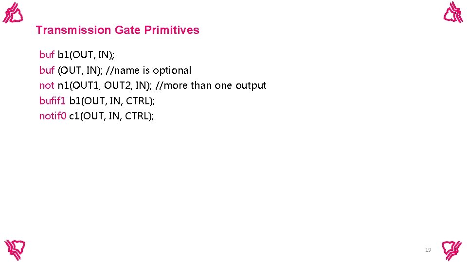
Transmission Gate Primitives buf b 1(OUT, IN); buf (OUT, IN); //name is optional not n 1(OUT 1, OUT 2, IN); //more than one output bufif 1 b 1(OUT, IN, CTRL); notif 0 c 1(OUT, IN, CTRL); 19
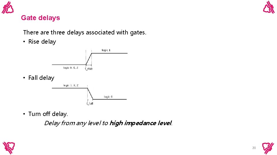
Gate delays There are three delays associated with gates. • Rise delay • Fall delay • Turn off delay. Delay from any level to high impedance level. 20
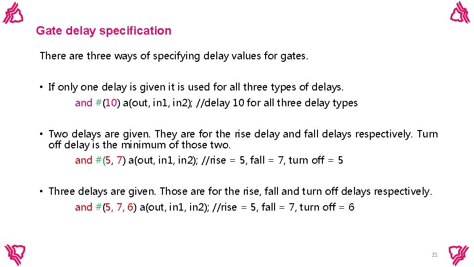
Gate delay specification There are three ways of specifying delay values for gates. • If only one delay is given it is used for all three types of delays. and #(10) a(out, in 1, in 2); //delay 10 for all three delay types • Two delays are given. They are for the rise delay and fall delays respectively. Turn off delay is the minimum of those two. and #(5, 7) a(out, in 1, in 2); //rise = 5, fall = 7, turn off = 5 • Three delays are given. Those are for the rise, fall and turn off delays respectively. and #(5, 7, 6) a(out, in 1, in 2); //rise = 5, fall = 7, turn off = 6 21
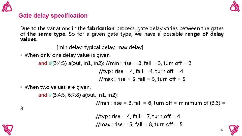
Gate delay specification Due to the variations in the fabrication process, gate delay varies between the gates of the same type. So for a given gate type, we have a possible range of delay values. [min delay: typical delay: max delay] • When only one delay value is given. and #(3: 4: 5) a(out, in 1, in 2); //min : rise = 3, fall = 3, turn off = 3 //typ : rise = 4, fall = 4, turn off = 4 //max : rise = 5, fall = 5, turn off = 5 • When two values are given. and #(3: 4: 5, 6: 7: 8) a(out, in 1, in 2); 3 //min : rise = 3, fall = 6, turn off = minimum of (3, 6) = //typ : rise = 4, fall = 7, turn off = 4 //max : rise = 5, fall = 8, turn off = 5 22
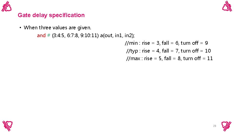
Gate delay specification • When three values are given. and # (3: 4: 5, 6: 7: 8, 9: 10: 11) a(out, in 1, in 2); //min : rise = 3, fall = 6, turn off = 9 //typ : rise = 4, fall = 7, turn off = 10 //max : rise = 5, fall = 8, turn off = 11 23
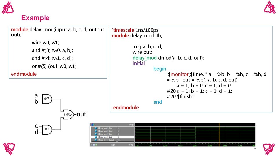
Example module delay_mod(input a, b, c, d, output out); wire w 0, w 1; and #(3) (w 0, a, b); and #(4) (w 1, c, d); or #(5) (out, w 0, w 1); endmodule `timescale 1 ns/100 ps module delay_mod_tb; reg a, b, c, d; wire out; delay_mod dmod(a, b, c, d, out); initial begin $monitor($time, " a = %b, b = %b, c = %b, d = %b out = %b", a, b, c, d, out); a = 0; b = 0; c = 0; d = 0; #20 a = 1; b = 1; c = 1; d = 1; #20 $finish; endmodule 24

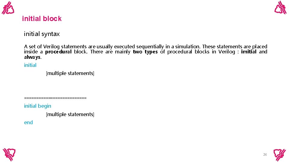
initial block initial syntax A set of Verilog statements are usually executed sequentially in a simulation. These statements are placed inside a procedural block. There are mainly two types of procedural blocks in Verilog : imitial and always. initial [multiple statements] ============= initial begin [multiple statements] end 26
initial block • An initial block is not synthesizable and hence cannot be converted into a hardware schematic with digital elements. • Initial blocks do not serve much purpose than to be used in simulations. • These blocks are primarily used to initialize variables and drive design ports with specific values. When does an initial block start and end? • Initial block is started at the beginning of a simulation at time 0 unit. This block will be executed only once during the entire simulation. • Execution of an executed. block finishes once all the statements within the block are 27
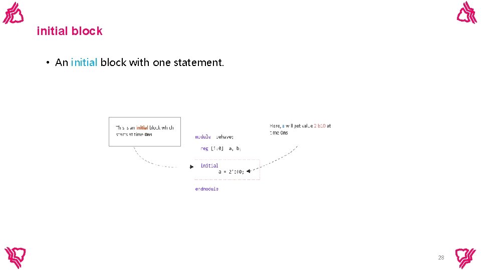
initial block • An initial block with one statement. 28
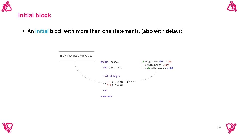
initial block • An initial block with more than one statements. (also with delays) 29
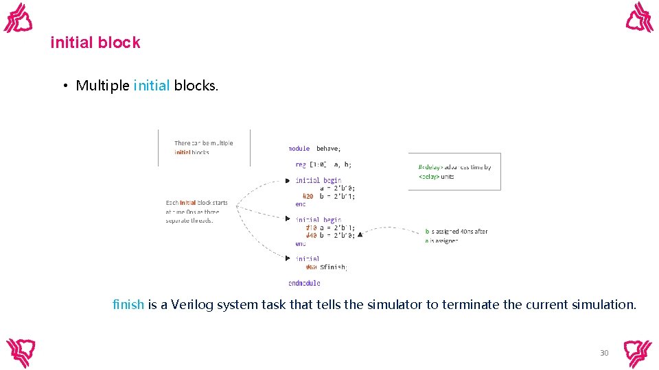
initial block • Multiple initial blocks. finish is a Verilog system task that tells the simulator to terminate the current simulation. 30
![initial block module initbegin; reg [1: 0] a, b, c, d; Initial begin initial initial block module initbegin; reg [1: 0] a, b, c, d; Initial begin initial](http://slidetodoc.com/presentation_image_h2/4572778732a3e2be6e94df25f11134be/image-31.jpg)
initial block module initbegin; reg [1: 0] a, b, c, d; Initial begin initial begin a=2'b 00; b=2'b 01; $display(“In the first initial a=%b, b=%b, time is %0 t", a, b, $time); end c=2'b 0; d=2'b 11; $display(“In the second initial c=%b, d=%b, time is %0 t", c, d, $time); end initial endmodule #60 $finish; 31
![initial block module initbegin 1; reg [1: 0] a, b; initial begin end initial initial block module initbegin 1; reg [1: 0] a, b; initial begin end initial](http://slidetodoc.com/presentation_image_h2/4572778732a3e2be6e94df25f11134be/image-32.jpg)
initial block module initbegin 1; reg [1: 0] a, b; initial begin end initial endmodule a=2'b 00; #20 b=2'b 00; #10 a=2'b 01; #20 b=2'b 01; #60 $finish; 32
![initial block module initbegin 1; reg [1: 0] a, b; initial begin end initial initial block module initbegin 1; reg [1: 0] a, b; initial begin end initial](http://slidetodoc.com/presentation_image_h2/4572778732a3e2be6e94df25f11134be/image-33.jpg)
initial block module initbegin 1; reg [1: 0] a, b; initial begin end initial endmodule a=2'b 00; #10 b=2'b 00; #10 a=2'b 01; #20 b=2'b 01; #60 $finish; 33
![initial block module initbegin 2; reg [1: 0] a, b; initial begin end initial initial block module initbegin 2; reg [1: 0] a, b; initial begin end initial](http://slidetodoc.com/presentation_image_h2/4572778732a3e2be6e94df25f11134be/image-34.jpg)
initial block module initbegin 2; reg [1: 0] a, b; initial begin end initial endmodule #10 a=2'b 00; #10 b=2'b 00; #10 a=2'b 01; #20 b=2'b 01; #60 $finish; 34
![initial block module initbegin 3; reg [1: 0] a, b; initial begin end initial initial block module initbegin 3; reg [1: 0] a, b; initial begin end initial](http://slidetodoc.com/presentation_image_h2/4572778732a3e2be6e94df25f11134be/image-35.jpg)
initial block module initbegin 3; reg [1: 0] a, b; initial begin end initial endmodule #10 a=2'b 01; #20 b=2'b 01; #10 a=2'b 00; #10 b=2'b 00; #60 $finish; 35
Strengths can be used to resolve which value should appear on a net or gate output. A strength specification shall have the following two components: • The strength of the 0 portion of the net value, called strength 0, designated as one of the following: supply 0 strong 0 pull 0 weak 0 highz 0 • The strength of the 1 portion of the net value, called strength 1, designated as one of the following: supply 1 strong 1 pull 1 weak 1 highz 1 • The combinations (highz 0, highz 1) and (highz 1, highz 0) shall be considered illegal. • There are four driving strengths: supply strong pull weak. Signals with driving strengths shall propagate from gate outputs and continuous assignment outputs. • There are three charge storage strengths: large medium small. Signals with the charge storage strengths are for trireg net type only. ( ex. trireg (small) p; ) 36
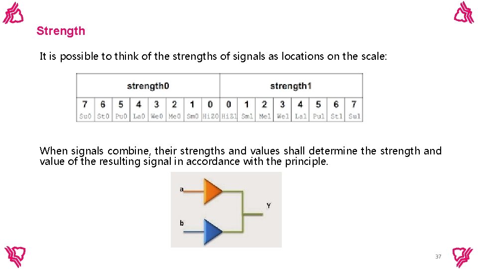
Strength It is possible to think of the strengths of signals as locations on the scale: When signals combine, their strengths and values shall determine the strength and value of the resulting signal in accordance with the principle. 37
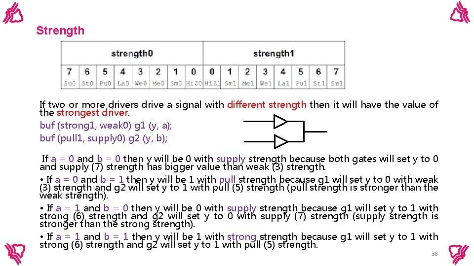
Strength If two or more drivers drive a signal with different strength then it will have the value of the strongest driver. buf (strong 1, weak 0) g 1 (y, a); buf (pull 1, supply 0) g 2 (y, b); If a = 0 and b = 0 then y will be 0 with supply strength because both gates will set y to 0 and supply (7) strength has bigger value than weak (3) strength. • If a = 0 and b = 1 then y will be 1 with pull strength because g 1 will set y to 0 with weak (3) strength and g 2 will set y to 1 with pull (5) strength (pull strength is stronger than the weak strength). • If a = 1 and b = 0 then y will be 0 with supply strength because g 1 will set y to 1 with strong (6) strength and g 2 will set y to 0 with supply (7) strength (supply strength is stronger than the strong strength). • If a = 1 and b = 1 then y will be 1 with strong strength because g 1 will set y to 1 with strong (6) strength and g 2 will set y to 1 with pull (5) strength. 38
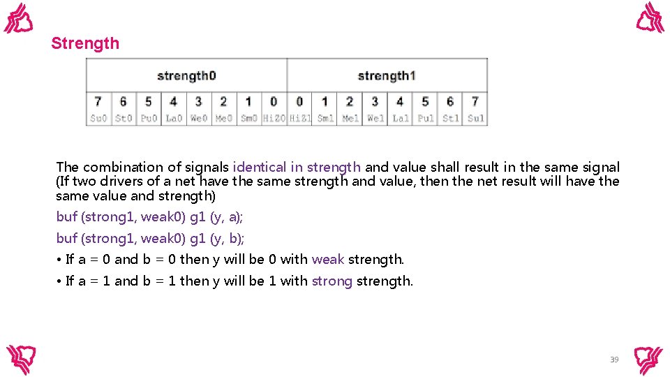
Strength The combination of signals identical in strength and value shall result in the same signal (If two drivers of a net have the same strength and value, then the net result will have the same value and strength) buf (strong 1, weak 0) g 1 (y, a); buf (strong 1, weak 0) g 1 (y, b); • If a = 0 and b = 0 then y will be 0 with weak strength. • If a = 1 and b = 1 then y will be 1 with strong strength. 39
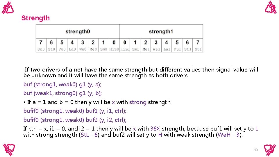
Strength If two drivers of a net have the same strength but different values then signal value will be unknown and it will have the same strength as both drivers buf (strong 1, weak 0) g 1 (y, a); buf (weak 1, strong 0) g 1 (y, b); • If a = 1 and b = 0 then y will be x with strong strength. bufif 0 (strong 1, weak 0) buf 1 (y, i 1, ctrl); bufif 0 (strong 1, weak 0) buf 2 (y, i 2, ctrl); If ctrl = x, i 1 = 0, and i 2 = 1 then y will be x with 36 X strength, because buf 1 will set y to L with strong strength (St. L - 6) and buf 2 will set y to H with weak strength (We. H - 3). 40
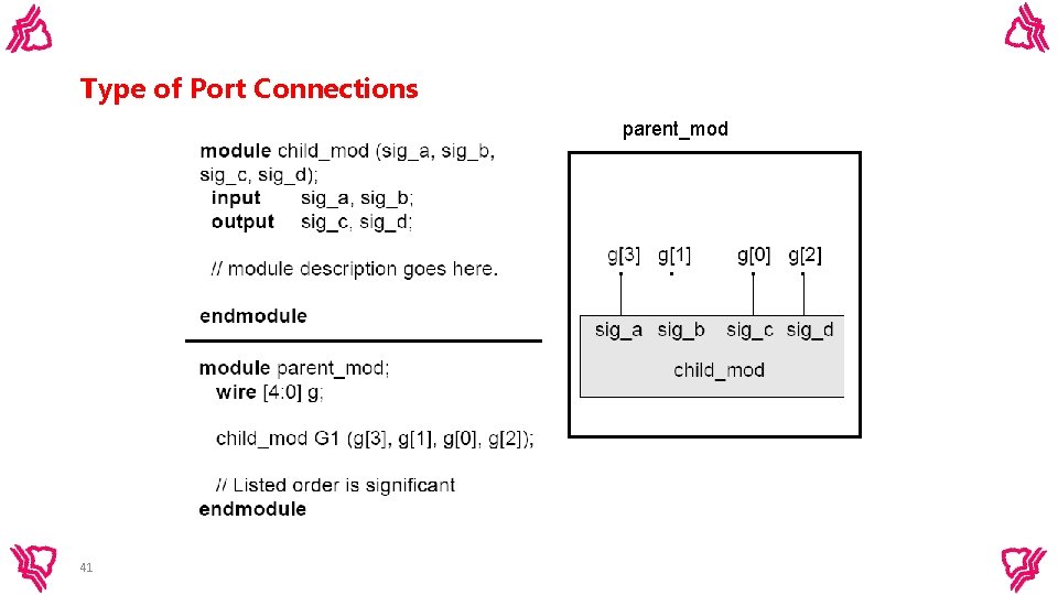
Type of Port Connections parent_mod 41
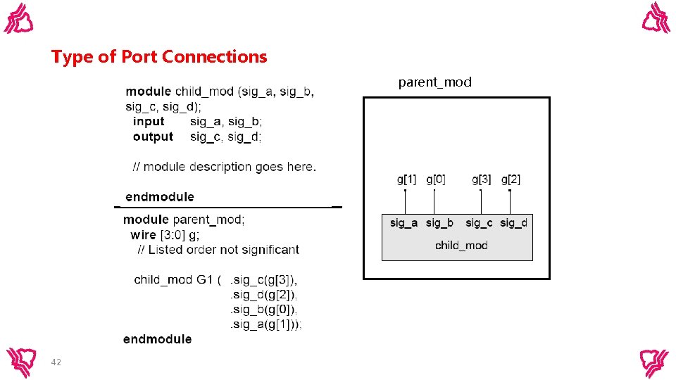
Type of Port Connections parent_mod 42
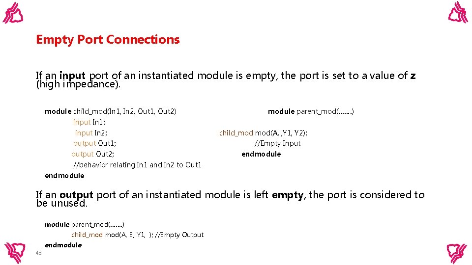
Empty Port Connections If an input port of an instantiated module is empty, the port is set to a value of z (high impedance). module child_mod(In 1, In 2, Out 1, Out 2) module parent_mod(……. ) input In 1; input In 2; output Out 1; output Out 2; child_mod mod(A, , Y 1, Y 2); //Empty Input endmodule //behavior relating In 1 and In 2 to Out 1 endmodule If an output port of an instantiated module is left empty, the port is considered to be unused. module parent_mod(……. ) child_mod mod(A, B, Y 1, ); //Empty Output endmodule 43
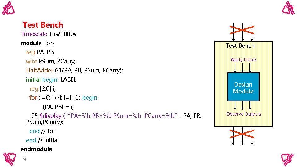
Test Bench `timescale 1 ns/100 ps module Top; reg PA, PB; wire PSum, PCarry; Test Bench Apply Inputs Half. Adder G 1(PA, PB, PSum, PCarry); initial begin: LABEL reg [2: 0] i; for (i=0; i<4; i=i+1) begin Design Module {PA, PB} = i; #5 $display (“PA=%b PB=%b PSum=%b PCarry=%b”, PA, PB, PSum, PCarry); end // for end // initial endmodule 44 Observe Outputs
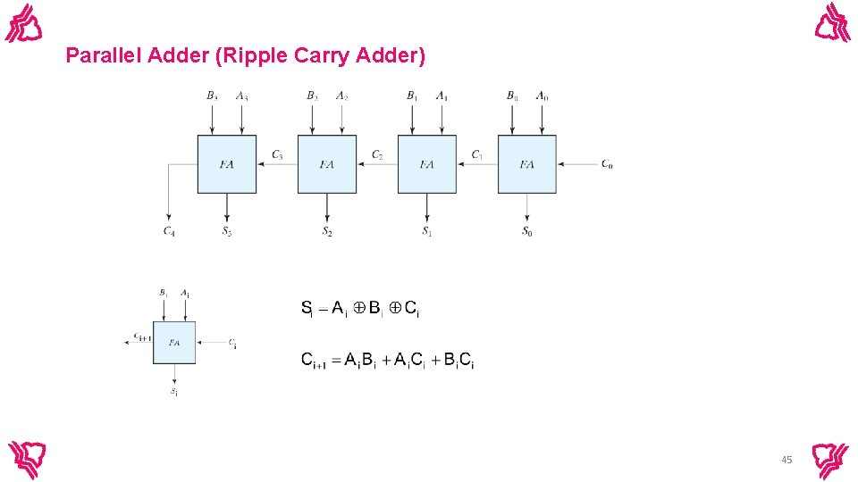
Parallel Adder (Ripple Carry Adder) 45

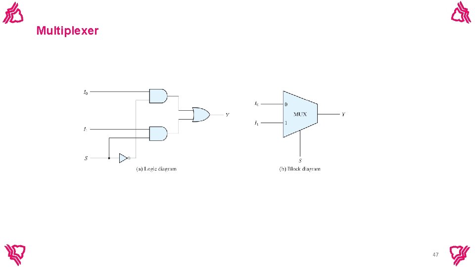
Multiplexer 47
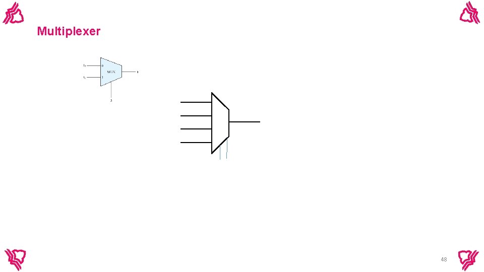
Multiplexer 48
Hazard 49
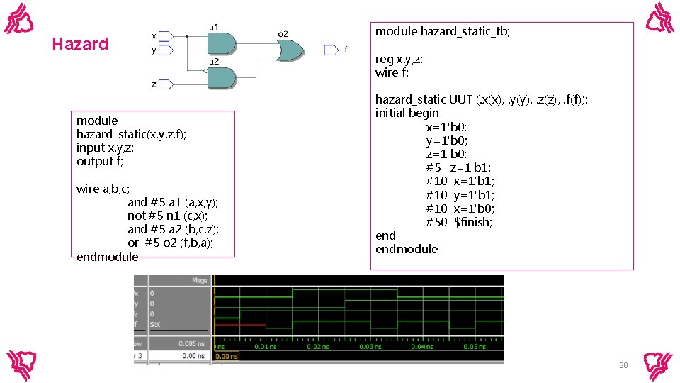
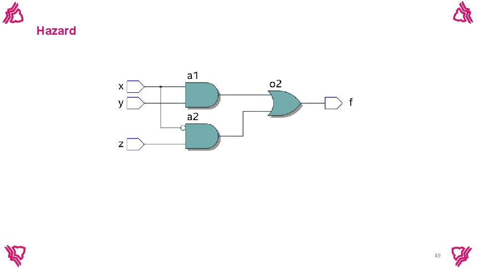
Hazard module hazard_static(x, y, z, f); input x, y, z; output f; wire a, b, c; and #5 a 1 (a, x, y); not #5 n 1 (c, x); and #5 a 2 (b, c, z); or #5 o 2 (f, b, a); endmodule hazard_static_tb; reg x, y, z; wire f; hazard_static UUT (. x(x), . y(y), . z(z), . f(f)); initial begin x=1'b 0; y=1'b 0; z=1'b 0; #5 z=1'b 1; #10 x=1'b 1; #10 y=1'b 1; #10 x=1'b 0; #50 $finish; endmodule 50
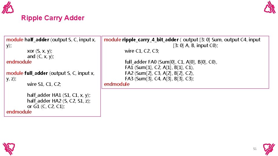
Ripple Carry Adder module half_adder (output S, C, input x, y); xor (S, x, y); and (C, x, y); endmodule full_adder (output S, C, input x, y, z); wire S 1, C 2; module ripple_carry_4_bit_adder ( output [3: 0] Sum, output C 4, input [3: 0] A, B, input C 0); wire C 1, C 2, C 3; full_adder FA 0 (Sum[0], C 1, A[0], B[0], C 0), FA 1 (Sum[1], C 2, A[1], B[1], C 1), FA 2 (Sum[2], C 3, A[2], B[2], C 2), FA 3 (Sum[3], C 4, A[3], B[3], C 3); endmodule half_adder HA 1 (S 1, C 1, x, y); half_adder HA 2 (S, C 2, S 1, z); or G 1 (C, C 2, C 1); endmodule 51

Ripple Carry Adder 52

Ripple Carry Adder 53
User Defined Primitives • The logic gates used in Verilog descriptions with keywords and, or, etc. , are defined by the system and are referred to as system primitives. • The user can create additional primitives by defining them in tabular form. These types of circuits are referred to as user-defined primitives (UDPs). • One way of specifying a digital circuit in tabular form is by means of a truth table. UDP descriptions do not use the keyword pair module. . . endmodule. • Instead, they are declared with the keyword pair primitive. . . endprimitive. 54
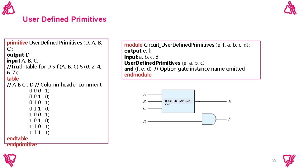
User Defined Primitives primitive User. Defined. Primitives (D, A, B, C); output D; input A, B, C; //Truth table for D 5 f (A, B, C) 5 (0, 2, 4, 6, 7); table // A B C : D // Column header comment 0 0 0 : 1; 0 0 1 : 0; 0 1 0 : 1; 0 1 1 : 0; 1 0 0 : 1; 1 0 1 : 0; 1 1 0 : 1; 1 1 1 : 1; endtable endprimitive module Circuit_User. Defined. Primitives (e, f, a, b, c, d); output e, f; input a, b, c, d User. Defined. Primitives (e, a, b, c); and (f, e, d); // Option gate instance name omitted endmodule User. Defined. Primiti ves 55
- Slides: 55