Contents 1 Overview 2 Lithography 3 Conclusion KNU
 2. 리소그래피 공정 (Lithography) 3. 결론 및 토의")

 Wafer Fabrication Assembly Test KNU")


 패턴")


 l UV 광이")


 식각이 얻어진다. ü 공정조건의 제어가")


![Lithography - Etch 식각 형태 Si + [O/F] a Si. F 4 (or Si.](https://slidetodoc.com/presentation_image_h/d6e6a6b75162488086c5b0f205d3a225/image-31.jpg "Lithography - Etch 식각 형태 Si + [O/F] a Si. F 4 (or Si.")

- Slides: 33
Contents 1. 반도체 제조 공정 (Overview) 2. 리소그래피 공정 (Lithography) 3. 결론 및 토의 (Conclusion) KNU Electrical Eng.
1. 반도체 제조 공정 KNU Electrical Eng.
Overview Logic Design Wafer Preparation Circuit Design Mask (Reticle) Wafer Fabrication Assembly Test KNU Electrical Eng.
Overview Logic & Circuit Design Crystal Growing KNU Ingot Slicing Mask Fab. Lapping & Polishing Electrical Eng. Wafer Fabrication
Overview Oxidation PR Coating Exposure Development Etching Metallization CVD Ion Implantation Assembly KNU Electrical Eng.
Overview KNU Test & Sorting Sawing Chip bonding Final test Molding Wire bonding Electrical Eng.
2. 리소그래피 공정 KNU Electrical Eng.
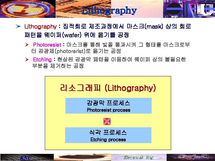
Lithography 감광막 프로세스 식각 프로세스 Photoresist process Etching process 감광막 도포 (PR coating) 패턴 식각 (pattern etching) 연화 건조 (soft bake) 감광막 제거 (PR strip) 마스크 정렬 (mask alignment) Next process 노광 (exposure) 현상 (develop) 경화 건조 (hard bake) KNU Electrical Eng. 10
Lithography Pattern Preparation Photoresist Coating Stepper Exposure Develop & Bake Acid Etch KNU Electrical Eng.
Lithography Positive Resist Si. O 2 Si Si Negative Resist Si. O 2 Mask Si. O 2 Si KNU Si. O 2 Si Electrical Eng. Si
Lithography Lithographic masking steps to produce Transistor KNU Electrical Eng.
Lithography - Photoresist Negative resist l high molecular weight polymer(MW~65, 000) l UV 광이 감응제(additive)에 흡수되면 N-N 결합이 깨어지고 대단히 활성 인 dangling bond가 생성 l 감응제가 다중체(polymer)와 가교(crosslink) 반응을 일으켜 노광된 감광 제(photoresist)는 현상액(developer)에 잘 녹지 않음 Positive resist l low molecular weight polymer(MW=5, 000~10, 000) l 감응제(inhibitor)가 첨가된 감광제는 현상액에 잘 녹지 않음 l UV 광이 감응제(inhibitor)에 흡수되면 구조적으로 재배열하여 산(acid)이 되고, 노광된 감광제는 현상액에 잘 녹음 KNU Electrical Eng. 15
Lithography - Photo Proximity & Contact Lithography Projection Lithography Illumination light Condenser lens Illumination light Mask pattern Diffracted light Projection lens gap Photoresist Wafer KNU Photoresist Wafer Electrical Eng.
Lithography - Photo E-Beam Directing Writing Lithography Electron source Illumination lens 1 st aperture Beam blanker Condenser lens 2 nd aperture Cell mask Beam Deflector Objective lens Wafer stage * Very Low throughput issue KNU Electrical Eng.
Lithography - Photo Next Generation of Lithography Technology ü X-Ray Lithography Resolution 좋지만, 비율 적용 불가 ü E-Beam Directing Lithography ü SCALPEL Lithography ü EUV Lithography ü Ion Beam Lithography KNU Resolution 좋지만 throughput 매우 낮다 E-beam + Mask Throughput, resolution 좋지만, Mirror 만들기 어렵다 (현실성 크다) 현실성 적다 Electrical Eng.
Lithography - Photo Key Technologies of Optical Lithography Technology Optical Form Resist Reticle Optical Materials Optical Coatings Optical Surfacing Stages Alignment Light Source Focus 248 193 157 EUV Technology Available Evolutionary Development R&D Required KNU Electrical Eng.
Lithography - Etch Lift-Off 가장 간단한 패턴 형성 공정 기술 q 적용 : 융점이 낮은 금속 등의 pattering 포토 공정 (Photo process) 박막 증착 (Thin film deposition) 감광막 제거 (PR strip) KNU Electrical Eng. 26
Lithography - Etch Wet Etching q 특징 ü 등방(isotropic) 식각이 얻어진다. ü 공정조건의 제어가 쉽지 않다. q 식각 용액 Si isotropic ; 1 HF : 3 HNO 3 : 8 CH 3 COOH 22℃ anisotropic ; KOH, Na. OH, EDP, Hydrazine(N 2 H 4 • H 2 O) 22℃ ☞ EDP: Ethylene Diamine[NH 2(CH 2)2 NH 2] + Pyrocatechol[C 6 H 4(OH)2] + H 2 O Si. O 2 KNU 7 NH 4 F : 1 HF Electrical Eng. 22℃ 27
Lithography - Etch Si 3 N 4 H 3 PO 4 155℃ poly-Si doped ; 200 HNO 3 : 80 CH 3 COOH : 1 HF 22℃ undoped ; 20 HNO 3 : 20 CH 3 COOH : 1 HF 22℃ Al 80 H 3 PO 4 : 5 HNO 3 : 5 CH 3 COOH : 10 H 2 O 22℃ q 감광막 제거 (PR strip) 4 H 2 SO 4 : 1 H 2 O 2 KNU 120℃ Electrical Eng. 10 min 28
Lithography - Etch < 10 -4 Torr 10 -4 ~ 10 -2 Torr 0. 1 ~ 1 Torr KNU Physical Sputtering (& Ion Beam Milling) • Physical momentum transfer (Ar) • Anisotropic possible • Poor selectivity • Radiation damage possible Reactive Ion Etching • Physical and chemical • Directional • More selective than sputtering Plasma Etching • Chemical, thus faster by 10 -1000 X • Isotropic • More selective Electrical Eng. 30
Lithography - Etch 식각 형태 Si + [O/F] a Si. F 4 (or Si. OF 2 or Si 2 OF 6) + O 2 + F 2 + CO 2 [O/F] : O 2 + {Cl 2 or SF 6 or CF 4} Si. O 2 + [O/F] a Si. F 4 (or Si. OF 2 or Si 2 OF 6) + O 2 + F 2 + CO 2 + H 2 O [O/F] : O 2 + {CF 4/H 2 or C 2 F 4 or C 3 F 6 or C 4 F 8} Si 3 N 4 + [O/F] a Si. F 4 (or Si. OF 2 or Si 2 OF 6) + O 2 + F 2 + CO 2 + H 2 O [O/F] : O 2 + {CF 4/H 2 or C 2 F 4 or C 3 F 6 or C 4 F 8} KNU Electrical Eng. 31
3. 결론 및 토의 KNU Electrical Eng.