Contact Info Name Email Tel Rm Wing Leong



- Slides: 72

Contact Info. • • Name: Email: Tel: Rm: Wing Leong, Chung (Zhong Rongliang, 锺荣亮) mfcchung@ust. hk 2358 7211 2130 A 1

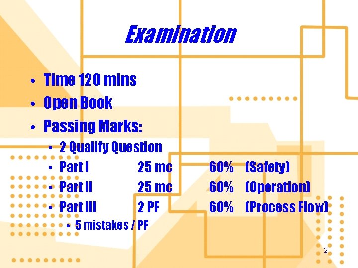
Examination • Time 120 mins • Open Book • Passing Marks: • • 2 Qualify Question Part I 25 mc Part III 2 PF 60% (Safety) 60% (Operation) 60% (Process Flow) • 5 mistakes / PF 2

NFF Operation Training Introduction 概引

Introduction 概引 • • • Contamination and Control 污染與管制 Process Flow 藝流程 Do’s and Don’t’s 規矩 Discussion on Exam Questions 考題討論 NFF Tour 參觀實驗所 4

NFF Operation Training Contamination and Control 污染與管制

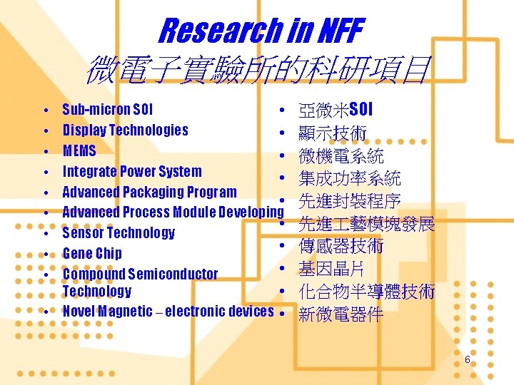
Research in NFF 微電子實驗所的科研項目 Sub-micron SOI • Display Technologies • MEMS • Integrate Power System • Advanced Packaging Program • Advanced Process Module Developing • Sensor Technology • Gene Chip • Compound Semiconductor • Technology • Novel Magnetic – electronic devices • • • 亞微米SOI 顯示技術 微機電系統 集成功率系統 先進封裝程序 先進 藝模塊發展 傳感器技術 基因晶片 化合物半導體技術 新微電器件 6

Outline • Contamination • Process Verification Scheme • Cleanliness Levels • Process Compatibility • Wafer Status • General Processing Requirements of Individual Modules • 污染 • 藝驗証指引 • 潔淨級別 • 藝兼容性 • 晶片潔淨指數 • 個別模組的要求 7

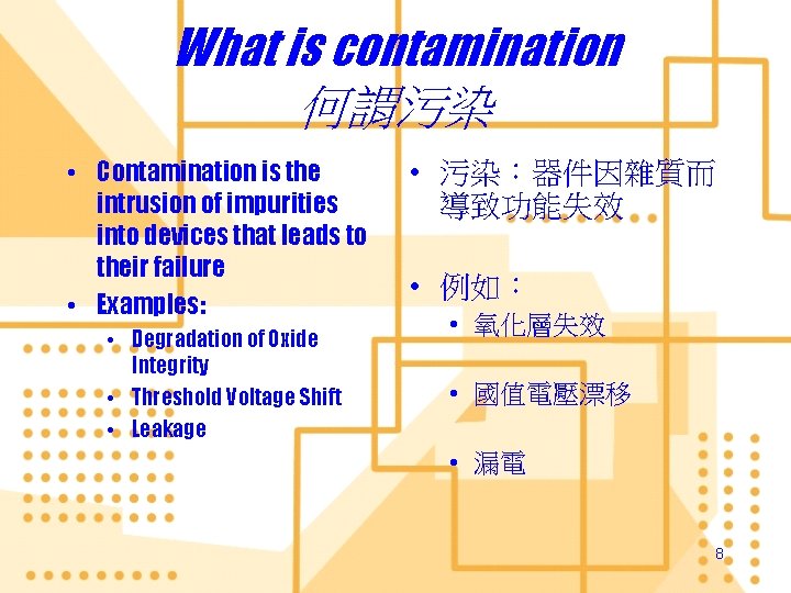
What is contamination 何謂污染 • Contamination is the intrusion of impurities into devices that leads to their failure • Examples: • Degradation of Oxide Integrity • Threshold Voltage Shift • Leakage • 污染:器件因雜質而 導致功能失效 • 例如: • 氧化層失效 • 國值電壓漂移 • 漏電 8

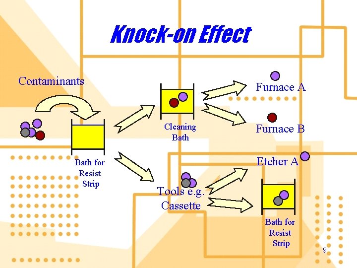
Knock-on Effect Contaminants Furnace A Cleaning Bath for Resist Strip Furnace B Etcher A Tools e. g. Cassette Bath for Resist Strip 9

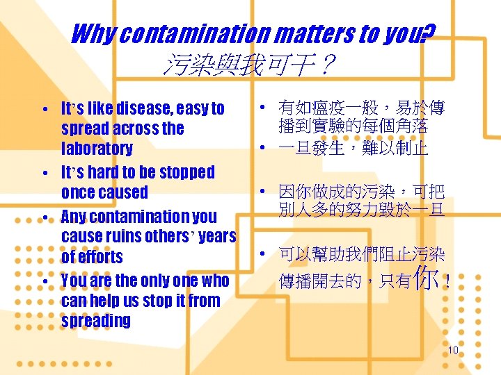
Why contamination matters to you? 污染與我可干? • It’s like disease, easy to spread across the laboratory • It’s hard to be stopped once caused • Any contamination you cause ruins others’ years of efforts • You are the only one who can help us stop it from spreading • 有如瘟疫一般,易於傳 播到實驗的每個角落 • 一旦發生,難以制止 • 因你做成的污染,可把 別人多的努力毀於一旦 • 可以幫助我們阻止污染 你! 傳播開去的,只有 10

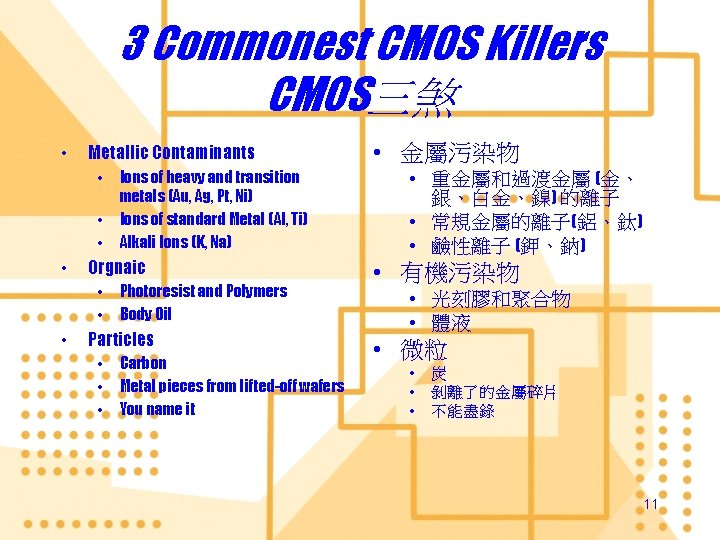
3 Commonest CMOS Killers CMOS三煞 • Metallic Contaminants • • Orgnaic • • • Ions of heavy and transition metals (Au, Ag, Pt, Ni) Ions of standard Metal (Al, Ti) Alkali Ions (K, Na) Photoresist and Polymers Body Oil Particles • • • Carbon Metal pieces from lifted-off wafers You name it • 金屬污染物 • 重金屬和過渡金屬 (金、 銀、白金、鎳) 的離子 • 常規金屬的離子(鋁、鈦) • 鹼性離子 (鉀、鈉) • 有機污染物 • 光刻膠和聚合物 • 體液 • 微粒 • • • 炭 剝離了的金屬碎片 不能盡錄 11

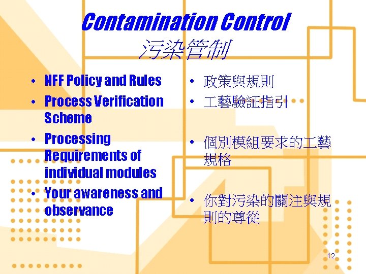
Contamination Control 污染管制 • NFF Policy and Rules • Process Verification Scheme • Processing Requirements of individual modules • Your awareness and observance • 政策與規則 • 藝驗証指引 • 個別模組要求的 藝 規格 • 你對污染的關注與規 則的尊從 12

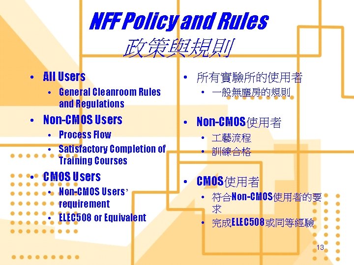
NFF Policy and Rules 政策與規則 • All Users • General Cleanroom Rules and Regulations • Non-CMOS Users • Process Flow • Satisfactory Completion of Training Courses • CMOS Users • Non-CMOS Users’ requirement • ELEC 508 or Equivalent • 所有實驗所的使用者 • 一般無塵房的規則 • Non-CMOS使用者 • 藝流程 • 訓練合格 • CMOS使用者 • 符合Non-CMOS使用者的要 求 • 完成ELEC 508或同等經驗 13

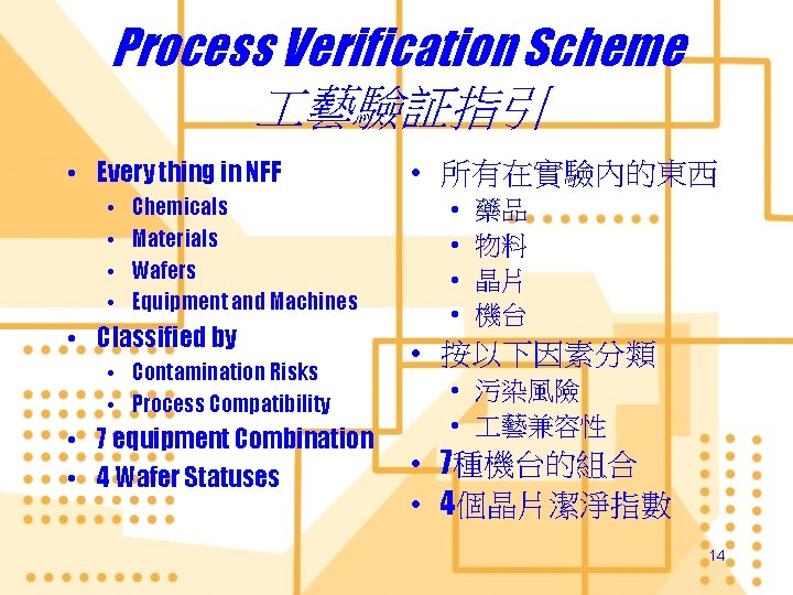
Process Verification Scheme 藝驗証指引 • Every thing in NFF • • Chemicals Materials Wafers Equipment and Machines • Classified by • Contamination Risks • Process Compatibility • 7 equipment Combination • 4 Wafer Statuses • 所有在實驗內的東西 • • 藥品 物料 晶片 機台 • 按以下因素分類 • 污染風險 • 藝兼容性 • 7種機台的組合 • 4個晶片潔淨指數 14

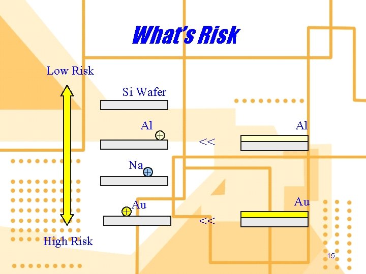
What’s Risk Low Risk Si Wafer Al Na + + Al << + Au Au << High Risk 15

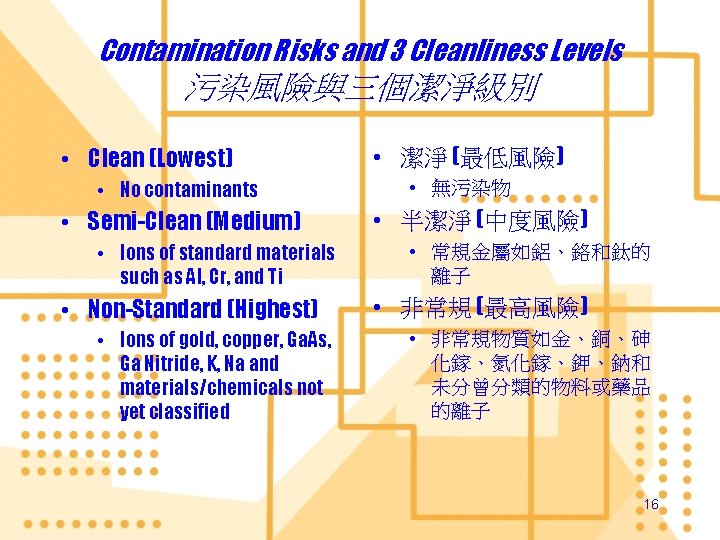
Contamination Risks and 3 Cleanliness Levels 污染風險與三個潔淨級別 • Clean (Lowest) • No contaminants • Semi-Clean (Medium) • Ions of standard materials such as Al, Cr, and Ti • Non-Standard (Highest) • Ions of gold, copper, Ga. As, Ga Nitride, K, Na and materials/chemicals not yet classified • 潔淨 (最低風險) • 無污染物 • 半潔淨 (中度風險) • 常規金屬如鋁、鉻和鈦的 離子 • 非常規 (最高風險) • 非常規物質如金、銅、砷 化鎵、氮化鎵、鉀、鈉和 未分曾分類的物料或藥品 的離子 16

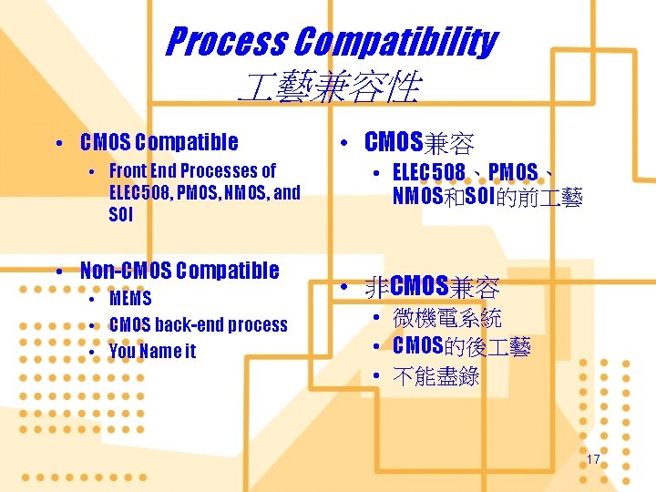
Process Compatibility 藝兼容性 • CMOS Compatible • Front End Processes of ELEC 508, PMOS, NMOS, and SOI • Non-CMOS Compatible • MEMS • CMOS back-end process • You Name it • CMOS兼容 • ELEC 508、PMOS、 NMOS和SOI的前 藝 • 非CMOS兼容 • 微機電系統 • CMOS的後 藝 • 不能盡錄 17

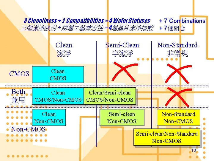
3 Cleanliness + 2 Compatibilities = 4 Wafer Statuses 三個潔淨級別 + 兩種 藝兼容性 = 4種晶片潔淨指數 Clean 潔淨 Non-Standard 非常規 Clean CMOS Both 兼用 Semi-Clean 半潔淨 + 7 Combinations + 7個組合 Clean/Semi-clean CMOS/Non-CMOS Clean Non-CMOS Semi-clean Non-CMOS Non-Standard Non-CMOS Semi-clean/Non-Standard Non-CMOS 18

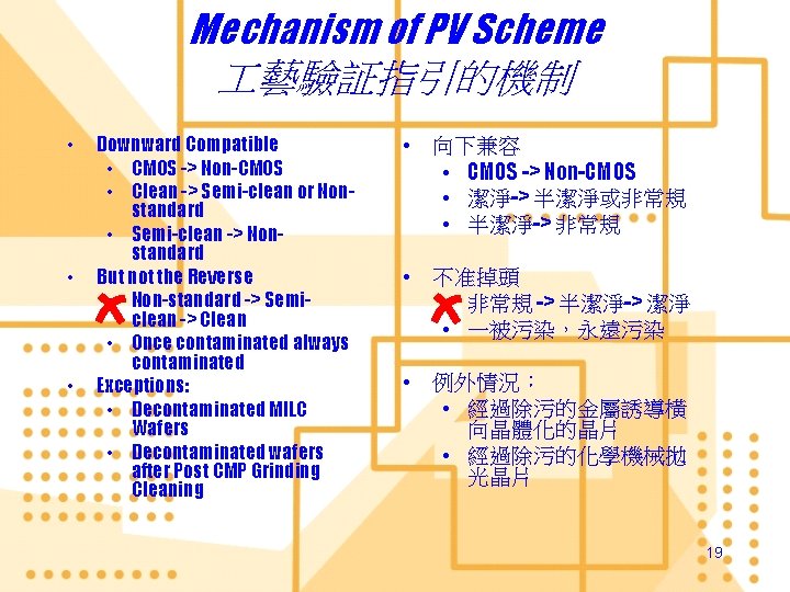
Mechanism of PV Scheme 藝驗証指引的機制 • • • Downward Compatible • CMOS -> Non-CMOS • Clean -> Semi-clean or Nonstandard • Semi-clean -> Nonstandard But not the Reverse • Non-standard -> Semiclean -> Clean • Once contaminated always contaminated Exceptions: • Decontaminated MILC Wafers • Decontaminated wafers after Post CMP Grinding Cleaning • 向下兼容 • CMOS -> Non-CMOS • 潔淨-> 半潔淨或非常規 • 半潔淨-> 非常規 • 不准掉頭 • 非常規 -> 半潔淨-> 潔淨 • 一被污染,永遠污染 • 例外情況: • 經過除污的金屬誘導橫 向晶體化的晶片 • 經過除污的化學機械拋 光晶片 19

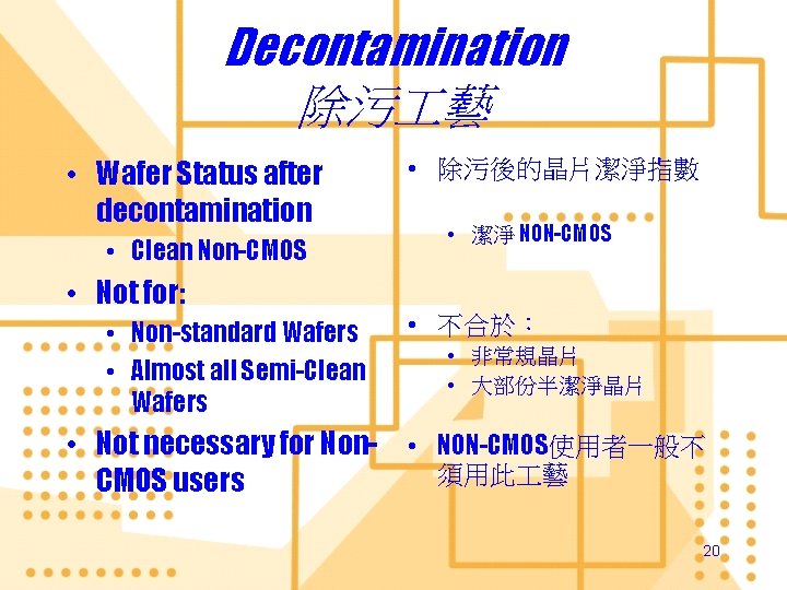
Decontamination 除污 藝 • Wafer Status after decontamination • Clean Non-CMOS • Not for: • Non-standard Wafers • Almost all Semi-Clean Wafers • 除污後的晶片潔淨指數 • 潔淨 NON-CMOS • 不合於: • 非常規晶片 • 大部份半潔淨晶片 • Not necessary for Non- • NON-CMOS使用者一般不 須用此 藝 CMOS users 20

Processing Requirements of individual processes 個別模組要求的 藝規格 • Wetstations • Oxidation, Diffusion and CVD • Implantation • Dry Etching • Sputtering • Photolithography • 濕化 藝台 • 氧化、擴散與化學汽 相澱積 • 離子注入 • 乾化蝕刻 • 濺射 • 光刻 21

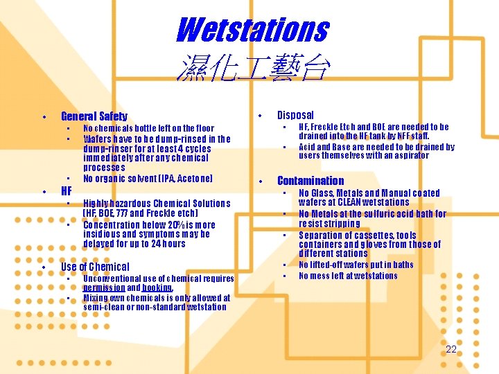
Wetstations 濕化 藝台 • General Safety • • HF • • • Wafers have to be dump-rinsed in the dump-rinser for at least 4 cycles immediately after any chemical processes No organic solvent (IPA, Acetone) Highly hazardous Chemical Solutions (HF, BOE, 777 and Freckle etch) Concentration below 20% is more insidious and symptoms may be delayed for up to 24 hours • Unconventional use of chemical requires permission and booking. Mixing own chemicals is only allowed at semi-clean or non-standard wetstation Disposal • No chemicals bottle left on the floor Use of Chemical • • HF, Freckle Etch and BOE are needed to be drained into the HF tank by NFF staff. Acid and Base are needed to be drained by users themselves with an aspirator Contamination • • • No Glass, Metals and Manual coated wafers at CLEAN wetstations No Metals at the sulfuric acid bath for resist stripping Separation of cassettes, tools containers and gloves from those of different stations No lifted-off wafers put in baths No mess left at wetstations 22

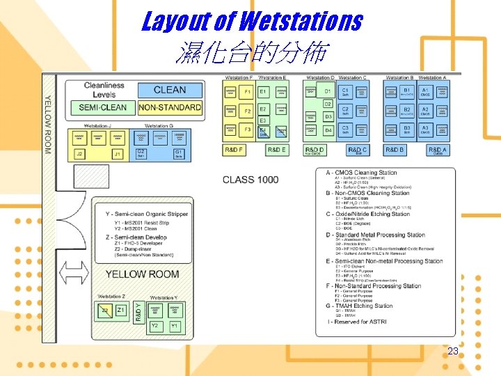
Layout of Wetstations 濕化台的分佈 23

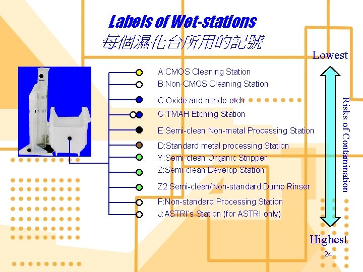
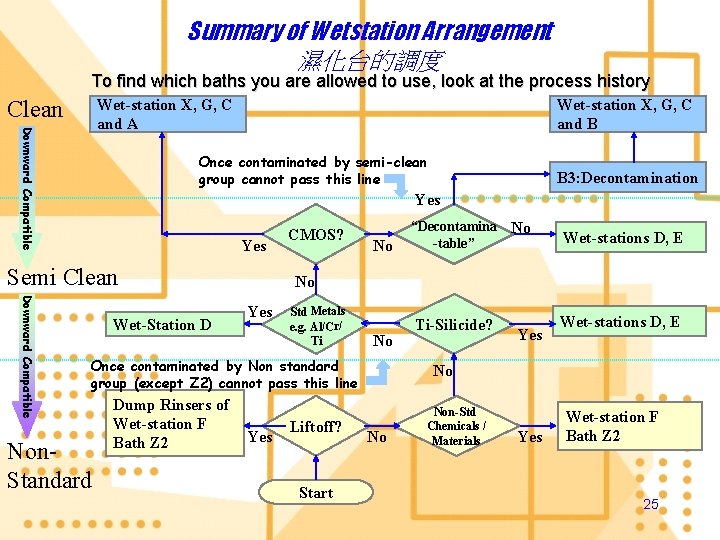
Labels of Wet-stations 每個濕化台所用的記號 Lowest A: CMOS Cleaning Station B: Non-CMOS Cleaning Station Risks of Contamination C: Oxide and nitride etch G: TMAH Etching Station E: Semi-clean Non-metal Processing Station D: Standard metal processing Station Y: Semi-clean Organic Stripper Z: Semi-clean Develop Station Z 2: Semi-clean/Non-standard Dump Rinser F: Non-standard Processing Station J: ASTRI’s Station (for ASTRI only) Highest 24

Summary of Wetstation Arrangement 濕化台的調度 To find which baths you are allowed to use, look at the process history Clean Downward Compatible Wet-station X, G, C and A Wet-station X, G, C and B Once contaminated by semi-clean group cannot pass this line B 3: Decontamination Yes Semi Clean Downward Compatible Wet-Station D CMOS? No Non. Standard No Wet-stations D, E No Yes Std Metals e. g. Al/Cr/ Ti No Once contaminated by Non standard group (except Z 2) cannot pass this line Dump Rinsers of Wet-station F Bath Z 2 “Decontamina -table” Yes Liftoff? Start Ti-Silicide? Yes Wet-stations D, E No No Non-Std Chemicals / Materials Yes Wet-station F Bath Z 2 25

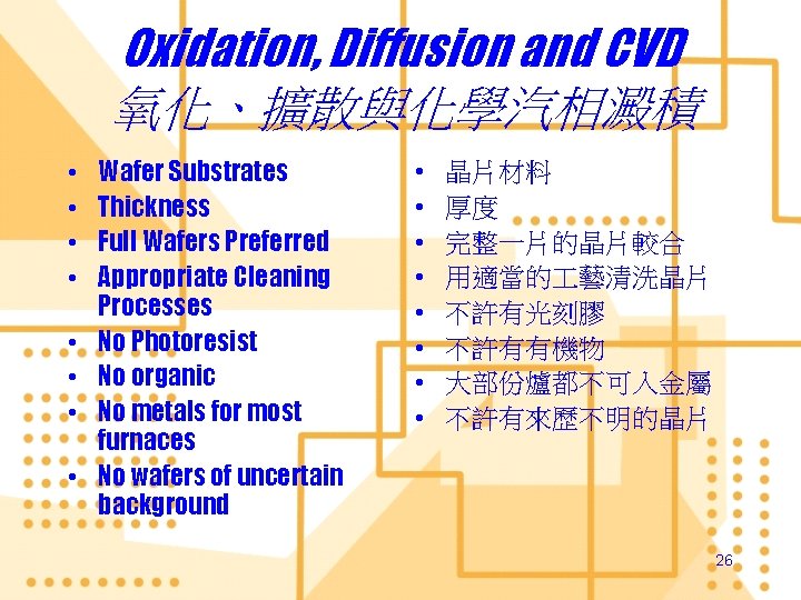
Oxidation, Diffusion and CVD 氧化、擴散與化學汽相澱積 • • Wafer Substrates Thickness Full Wafers Preferred Appropriate Cleaning Processes No Photoresist No organic No metals for most furnaces No wafers of uncertain background • • 晶片材料 厚度 完整一片的晶片較合 用適當的 藝清洗晶片 不許有光刻膠 不許有有機物 大部份爐都不可入金屬 不許有來歷不明的晶片 26

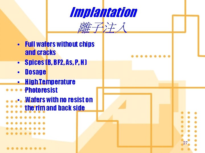
Implantation 離子注入 • Full wafers without chips and cracks • Spices (B, BF 2, As, P, H) • Dosage • High Temperature Photoresist • Wafers with no resist on the rim and back side 27

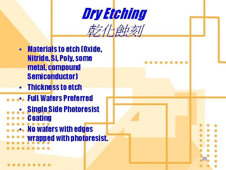
Dry Etching 乾化蝕刻 • Materials to etch (Oxide, Nitride, Si, Poly, some metal, compound Semiconductor) • Thickness to etch • Full Wafers Preferred • Single Side Photoresist Coating • No wafers with edges wrapped with photoresist. 28

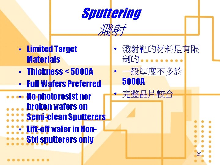
Sputtering 濺射 • 濺射靶的材料是有限 • Limited Target 制的 Materials • 一般厚度不多於 • Thickness < 5000 A • Full Wafers Preferred • 完整晶片較合 • No photoresist nor broken wafers on Semi-clean Sputterers • Lift-off wafer in Non. Std sputterers only 29

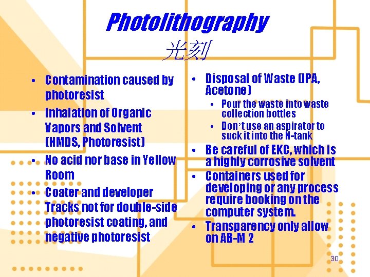
Photolithography 光刻 • Contamination caused by photoresist • Inhalation of Organic Vapors and Solvent (HMDS, Photoresist) • No acid nor base in Yellow Room • Coater and developer Tracks not for double-side photoresist coating, and negative photoresist • Disposal of Waste (IPA, Acetone) • Pour the waste into waste collection bottles • Don’t use an aspirator to suck it into the N-tank • Be careful of EKC, which is a highly corrosive solvent • Containers used for developing or any process require booking on the computer system. • Transparency only allow on AB-M 2 30

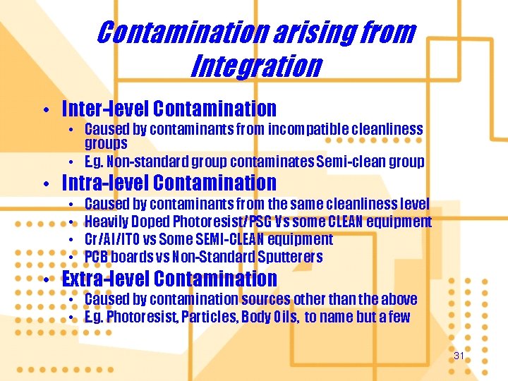
Contamination arising from Integration • Inter-level Contamination • Caused by contaminants from incompatible cleanliness groups • E. g. Non-standard group contaminates Semi-clean group • Intra-level Contamination • • Caused by contaminants from the same cleanliness level Heavily Doped Photoresist/PSG Vs some CLEAN equipment Cr/Al/ITO vs Some SEMI-CLEAN equipment PCB boards vs Non-Standard Sputterers • Extra-level Contamination • Caused by contamination sources other than the above • E. g. Photoresist, Particles, Body Oils, to name but a few 31

NFF Operation Training Process Flow 藝流程

Outline • • Aim Standard Format Common Mistakes Process Guidelines 33

Aim of Process Flows • Functions: • Help you to plan ahead • Track down wafer movement • Reduce uncertainty • keep the unqualified away from NFF • Aim: • Control Contamination 34

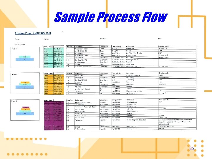
Sample Process Flow 35

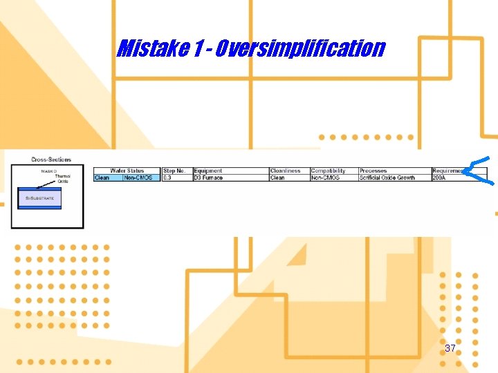
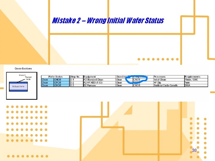
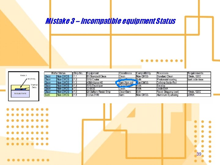
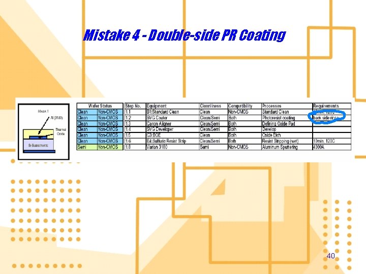
Standard Format • • • Heading Cross-sections Wafer Status Step no. Equipment Cleanliness Compatibility Processes Requirements 36

Mistake 1 - Oversimplification 37

Mistake 2 – Wrong Initial Wafer Status 38

Mistake 3 – Incompatible equipment Status 39

Mistake 4 - Double-side PR Coating 40

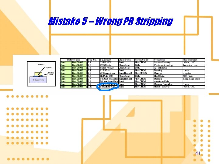
Mistake 5 – Wrong PR Stripping 41

Other Mistakes • Mistake 6 - Misuse of low stress nitride as oxidation masks • Mistake 7 – Misuse of Decontamination • Mistake 8 – Wafer Edge Coating • Mistake 9 – missing backside rinsing prior to implantation 42

Process Guidelines • 7 Cleanings • 4 Resist Stripping • Post-Deep Si Etch Polymer Removal • 3 Etchings to Etch Through Wafers • Liftoff • Non-standard Metal (Gold) 43

Cleanings • Sulfuric Clean (CMOS) • RCA 2(Decontamination) • Pre-diffusion Clean (CMOS) • Pre-deposition Clean (CMOS) • Sulfuric Clean (Non-CMOS) • Post-Metallization Clean • Mask Cleaning 44

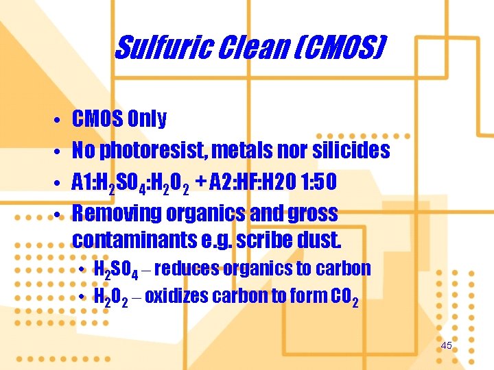
Sulfuric Clean (CMOS) • • CMOS Only No photoresist, metals nor silicides A 1: H 2 SO 4: H 2 O 2 + A 2: HF: H 2 O 1: 50 Removing organics and gross contaminants e. g. scribe dust. • H 2 SO 4 – reduces organics to carbon • H 2 O 2 – oxidizes carbon to form CO 2 45

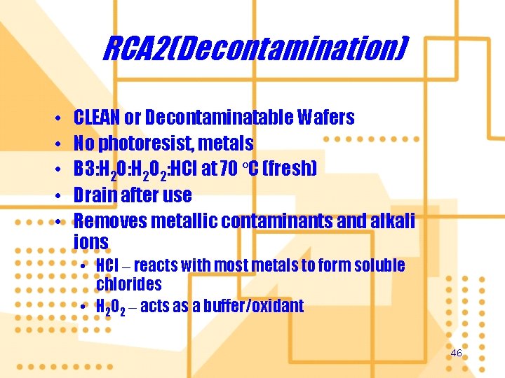
RCA 2(Decontamination) • • • CLEAN or Decontaminatable Wafers No photoresist, metals B 3: H 2 O 2: HCl at 70 ºC (fresh) Drain after use Removes metallic contaminants and alkali ions • HCl – reacts with most metals to form soluble chlorides • H 2 O 2 – acts as a buffer/oxidant 46

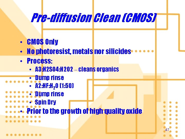
Pre-diffusion Clean (CMOS) • CMOS Only • No photoresist, metals nor silicides • Process: • • • A 3: H 2 SO 4: H 2 O 2 – cleans organics Dump rinse A 2: HF: H 2 O (1: 50) Dump rinse Spin Dry • Prior to the growth of high quality oxide 47

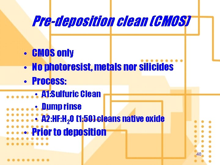
Pre-deposition clean (CMOS) • CMOS only • No photoresist, metals nor silicides • Process: • A 1: Sulfuric Clean • Dump rinse • A 2: HF: H 2 O (1: 50) cleans native oxide • Prior to deposition 48

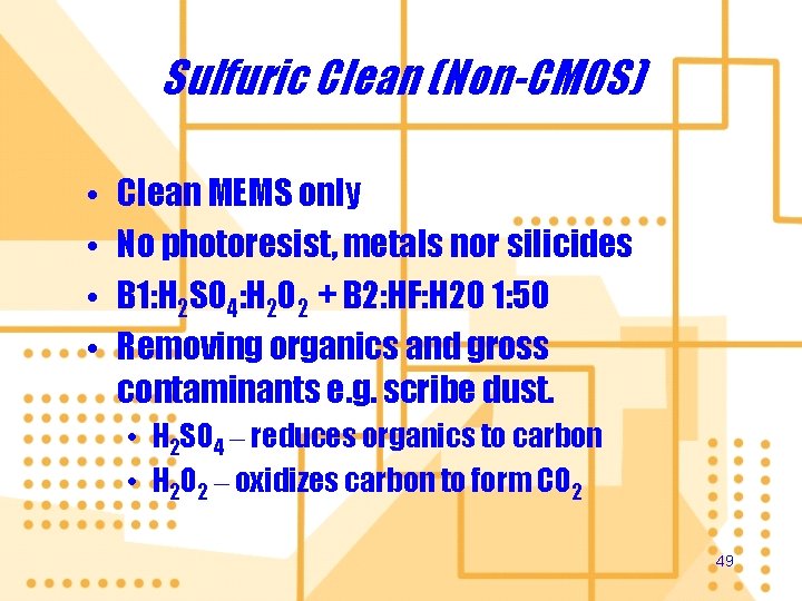
Sulfuric Clean (Non-CMOS) • • Clean MEMS only No photoresist, metals nor silicides B 1: H 2 SO 4: H 2 O 2 + B 2: HF: H 2 O 1: 50 Removing organics and gross contaminants e. g. scribe dust. • H 2 SO 4 – reduces organics to carbon • H 2 O 2 – oxidizes carbon to form CO 2 49

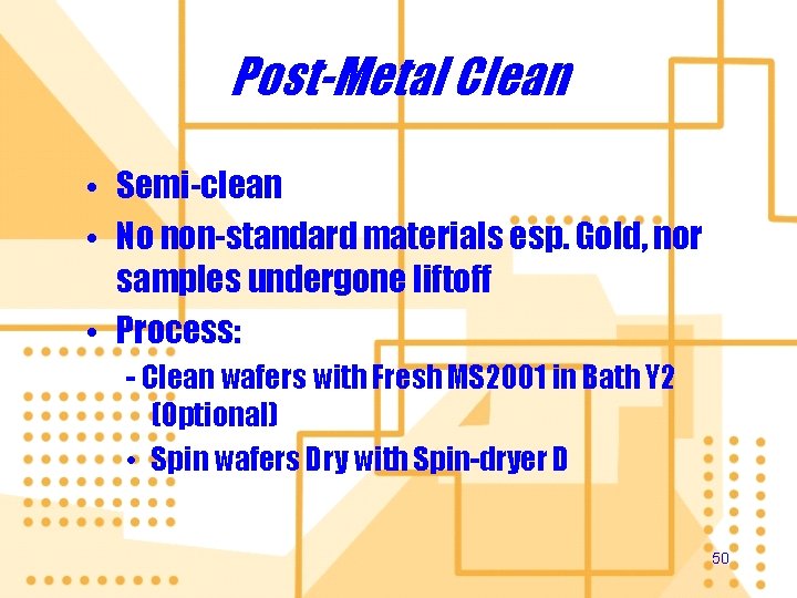
Post-Metal Clean • Semi-clean • No non-standard materials esp. Gold, nor samples undergone liftoff • Process: - Clean wafers with Fresh MS 2001 in Bath Y 2 (Optional) • Spin wafers Dry with Spin-dryer D 50

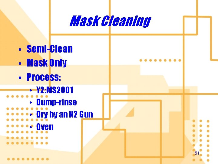
Mask Cleaning • Semi-Clean • Mask Only • Process: • • Y 2: MS 2001 Dump-rinse Dry by an N 2 Gun Oven 51

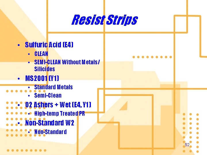
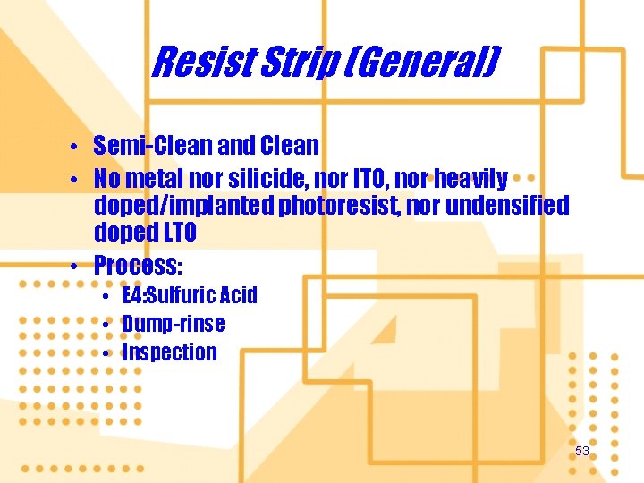
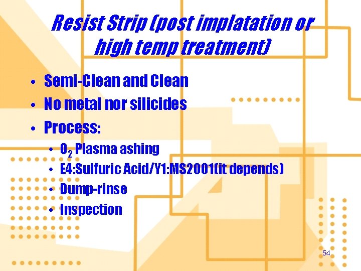
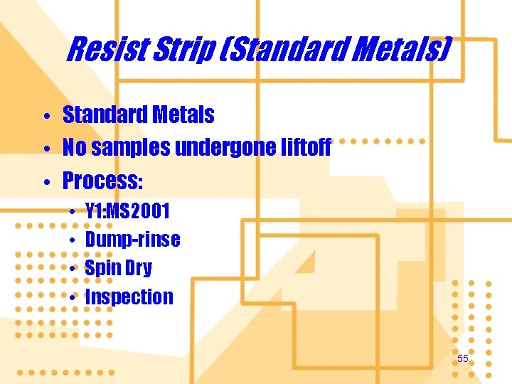
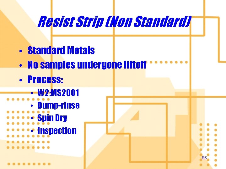
Resist Strips • Sulfuric Acid (E 4) • CLEAN • SEMI-CLEAN Without Metals/ Silicides • MS 2001 (Y 1) • Standard Metals • Semi-Clean • O 2 Ashers + Wet (E 4, Y 1) • High-temp Treated PR • Non-Standard W 2 • Non-Standard 52

Resist Strip (General) • Semi-Clean and Clean • No metal nor silicide, nor ITO, nor heavily doped/implanted photoresist, nor undensified doped LTO • Process: • E 4: Sulfuric Acid • Dump-rinse • Inspection 53

Resist Strip (post implatation or high temp treatment) • Semi-Clean and Clean • No metal nor silicides • Process: • • O 2 Plasma ashing E 4: Sulfuric Acid/Y 1: MS 2001(it depends) Dump-rinse Inspection 54

Resist Strip (Standard Metals) • Standard Metals • No samples undergone liftoff • Process: • • Y 1: MS 2001 Dump-rinse Spin Dry Inspection 55

Resist Strip (Non Standard) • Standard Metals • No samples undergone liftoff • Process: • • W 2: MS 2001 Dump-rinse Spin Dry Inspection 56

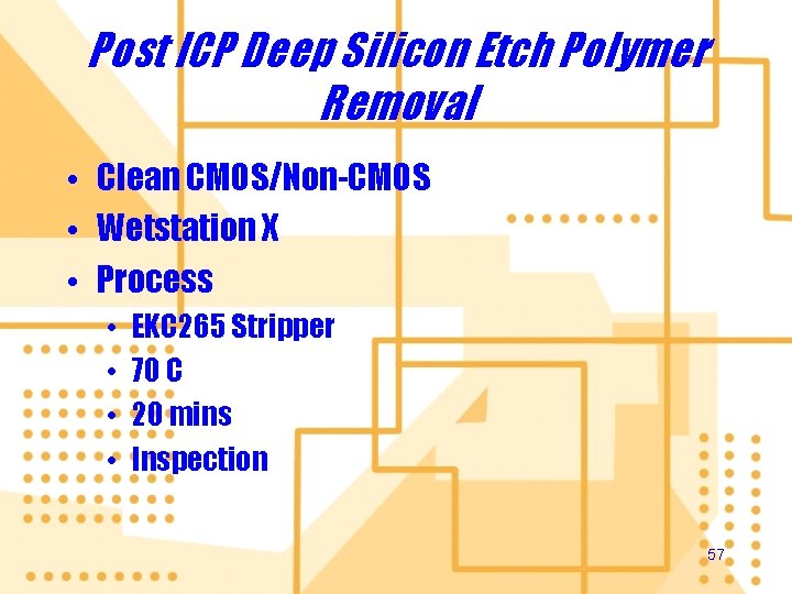
Post ICP Deep Silicon Etch Polymer Removal • Clean CMOS/Non-CMOS • Wetstation X • Process • • EKC 265 Stripper 70 C 20 mins Inspection 57

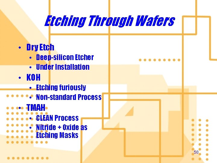
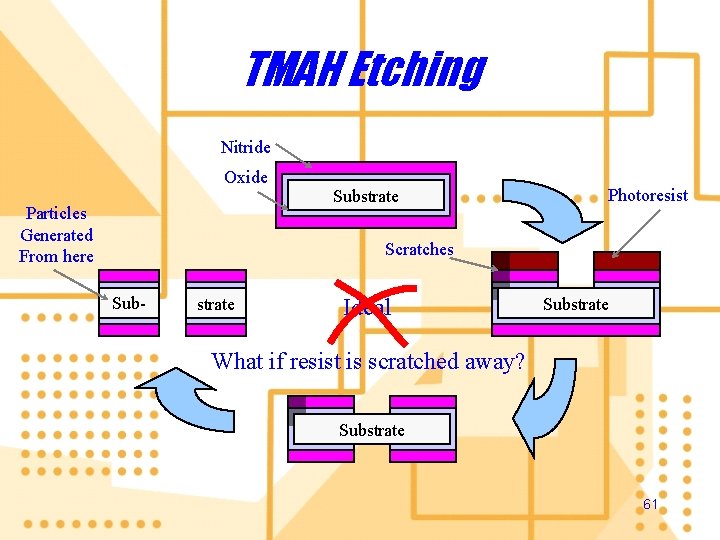
Etching Through Wafers • Dry Etch • Deep-silicon Etcher • Under Installation • KOH • Etching furiously • Non-standard Process • TMAH • CLEAN Process • Nitride + Oxide as Etching Masks 58

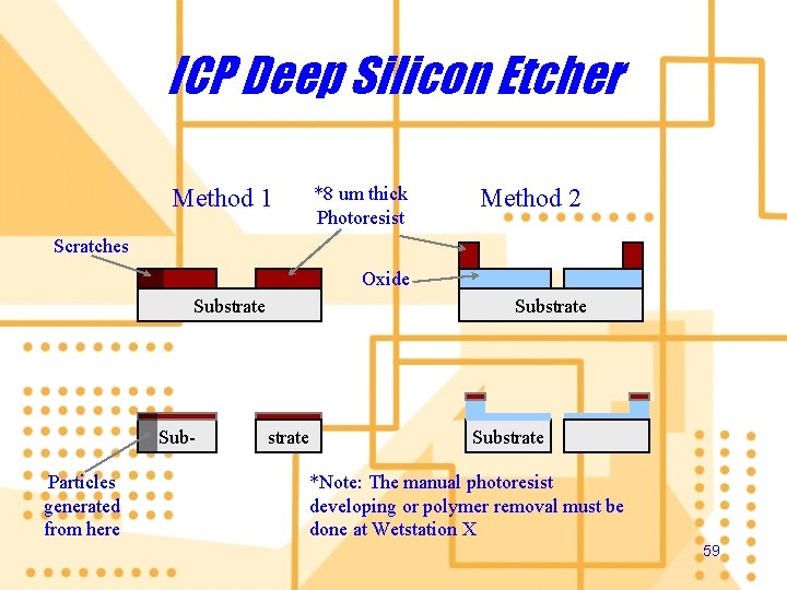
ICP Deep Silicon Etcher *8 um thick Photoresist Method 1 Method 2 Scratches Oxide Substrate Sub. Particles generated from here Substrate *Note: The manual photoresist developing or polymer removal must be done at Wetstation X 59

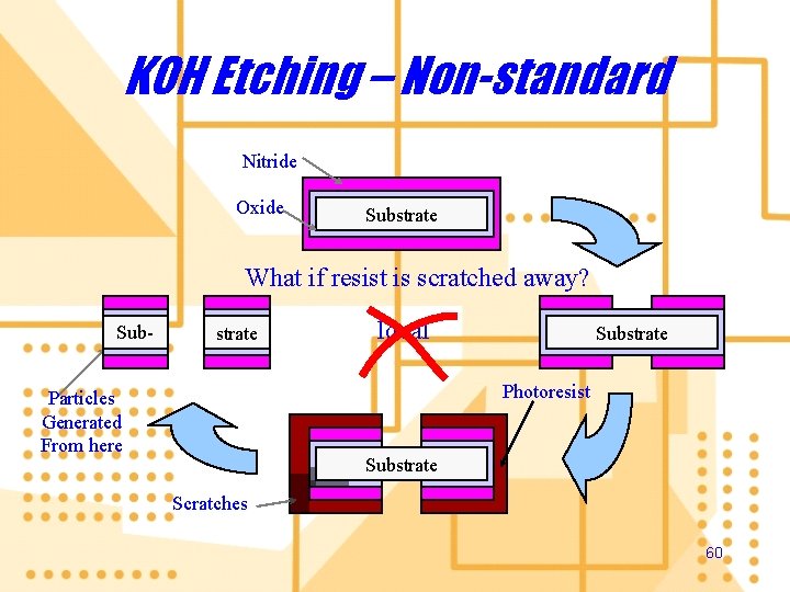
KOH Etching – Non-standard Nitride Oxide Substrate What if resist is scratched away? Sub- strate Ideal Substrate Photoresist Particles Generated From here Substrate Scratches 60

TMAH Etching Nitride Oxide Particles Generated From here Substrate Photoresist Scratches Sub- strate Ideal Substrate What if resist is scratched away? Substrate 61

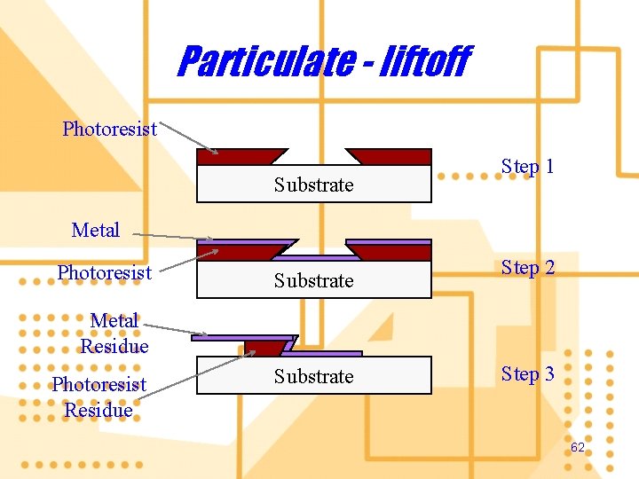
Particulate - liftoff Photoresist Substrate Step 1 Metal Photoresist Substrate Step 2 Metal Residue Photoresist Residue Substrate Step 3 62

Particulate – liftoff (con’t) • Guideline for liftoff process • Acetone, and IPA used should be poured into dedicated waste bottles • Make it the last step • Once liftoff is done, the samples can’t stop generating contaminants. • Don’t even think about putting samples into any processing baths, That is extremely irresponsible! 63

Metallic Contaminant – Gold • Gold Ions • Most-Contaminating because of its high mobility • Easy to spread into the atmosphere, if heated • From films, equipment, tools, containers and cassettes, which are in contact with Au+ ions • Totally incompatible with almost all processes and equipment except for • Bath Z 2 • Wetstation F • Thermco E 4: Thermal Anneal (Gold) 64

Metallic Contaminant – Gold • Guidelines for processing gold • Make it as close to the last step as possible. Once samples are gold-contaminated, you are banned from doing almost all processes. • Never put gold-contaminated samples into clean and semi-clean areas, (in particular sulfuric acid for resist stripping). Otherwise you will kill the whole laboratory! 65

NFF Operation Training Do’s and Don’t’s 規矩

Chemicals and Wetstations • Don’t bring your own chemicals or materials into NFF unless you have approval • Don’t take any chemicals or materials away. That is theft. • Don’t leave chemical bottles on the floor • Never put into CLEAN baths wafers that have undergone metallization. • Don’t leave anything, especially incompatible materials, on the top of wetstations. • Disposal of HF and BOE must be done by trained persons • • • Don’t be so irresponsible as to leave down the tools you have used and go away Don’t mix up the gloves, cassettes and tools of one station with those of others. You should look at the labels! Clean all the tools and containers you have used and place them back to where they are No ORGANIC Solvent at wetstations in Class 1000 No acid and base in Yellow Room 67

Operation • Store wafers of different wafer status in separate boxes • Always inspect your wafers after a resist strip to ensure cleanliness • Don’t put non-standard materials, especially gold into semi-clean and clean baths • Don’t put liftoff samples in any processing baths • • Always keep your samples in your own containers or cassette boxes in case they contaminate others or be contaminated. Always be careful with photoresist which is very contaminating. Arrange non-standard steps as close to the end of process flow as possible. After cleaning, wafers must go straight to furnaces without being touched by any objects 68

Process Flows • Plan before work. If you fail to plan you are planning to fail • Write what you do and do what you write. • Once your process becomes different from what you have planed, sumit us a new flow • Never copy others’ process flow • Never let others copy your process flow • Do let us know, if you find your processes departing from our scheme. • Proofread before submitting them 69

Personal • Don’t shortcut any policy and rules • Keep yourself abreast of information about rules and regulations, as it is dynamic and subject to change. • Report to us any mistakes you or others have made. Don’t hide it! • be aware of contamination that you may cause and others cause • Remember, this is a shared lab. Everyone must follow lab policy to keep it clean • Use your judgment. Avoid contamination of wafers or equipment • Don’t stay in the laboratory if not necessary. NFF is not a meeting place! 70

Useful Webpages • NFF User Guide (well underway) • Hook up to http: //www. nff. ust. hk and then click on “Safety course registration” or • http: //www. nff. ust. hk/mffdoc/index. htm • NFF Booking System • https: //www. nff. ust. hk/booking • Material Request Form • Logon NFF Booking System and then click on “User Info” • Other process information • http: //mfk 060. ust. hk 71

NFF Operation Training Q&A 答問時間