Congruence Structure of Synchronous Mirror Delay As a

- Slides: 42

Congruence Structure of Synchronous Mirror Delay As a Case of Research Method for Students in CSIE Tsung-Chu Huang Dept. of Electronic Eng. National Changhua University of Ed. Email: tch@cc. ncue. edu. tw 2004/12/15 Talk@CSIE. DYU TC Huang, NCUE 2004/12/15

Outline • • • Introduction Previous Work Proposed Congruence SMD Structure Experimental Results Applications of Proposed SMDs Conclusion and Future Work TC Huang, NCUE 2004/12/15 2

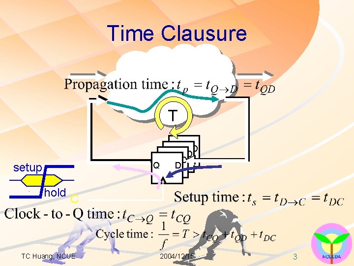
Time Clausure T Q D Q D setup hold C TC Huang, NCUE 2004/12/15 3

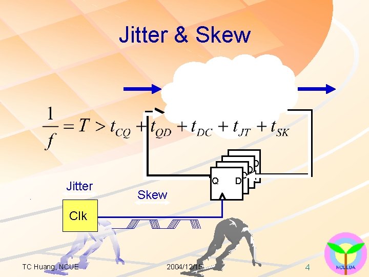
Jitter & Skew Jitter Q D Q D Skew Clk TC Huang, NCUE 2004/12/15 4

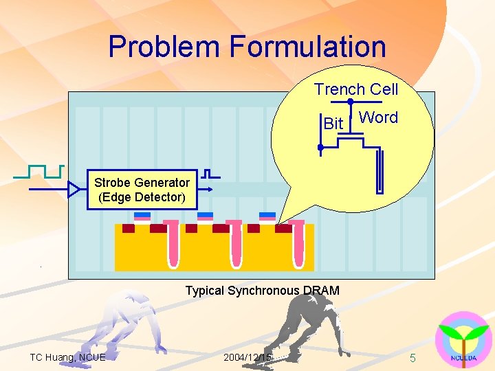
Problem Formulation Trench Cell Bit Word Strobe Generator (Edge Detector) Typical Synchronous DRAM TC Huang, NCUE 2004/12/15 5

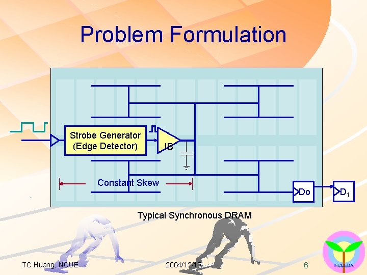
Problem Formulation Strobe Generator (Edge Detector) IB Constant Skew Do Typical Synchronous DRAM TC Huang, NCUE 2004/12/15 6 D 1

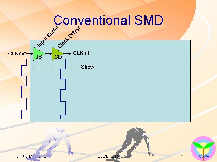
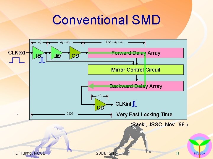
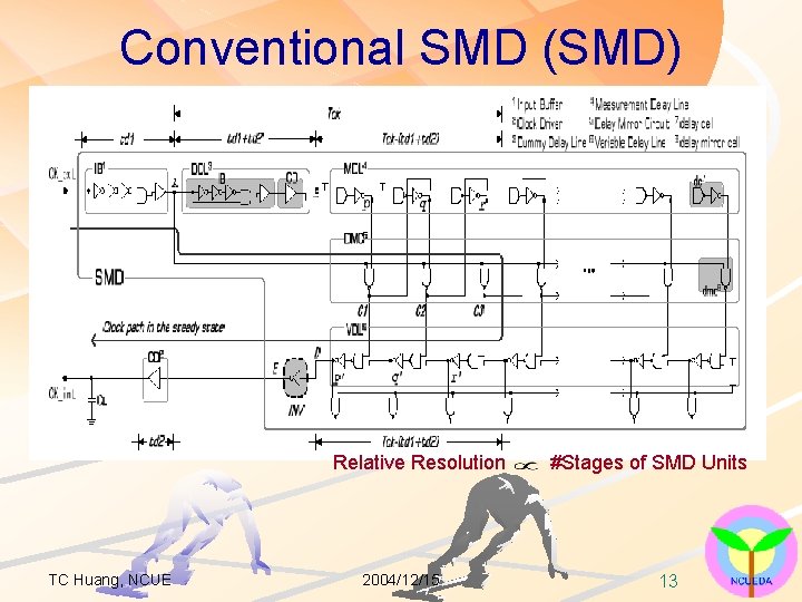
Conventional SMD r er e f t u p n I CLKext IB f u B k c lo riv D C CD CLKint Skew TC Huang, NCUE 2004/12/15 7

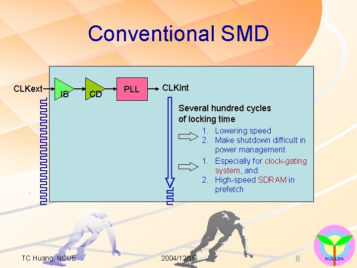
Conventional SMD CLKext IB CD PLL CLKint Several hundred cycles of locking time 1. Lowering speed 2. Make shutdown difficult in power management 1. Especially for clock-gating system, and 2. High-speed SDRAM in prefetch TC Huang, NCUE 2004/12/15 8

Conventional SMD CLKext IB IB CD Forward Delay Array CD Mirror Control Circuit Backward Delay Array CD CLKint Very Fast Locking Time (Saeki, JSSC, Nov. ’ 96. ) TC Huang, NCUE 2004/12/15 9

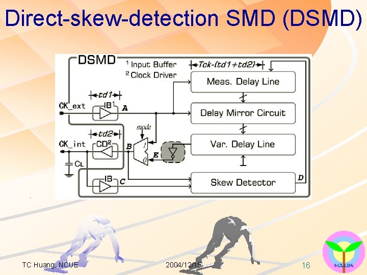
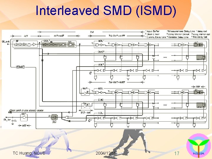
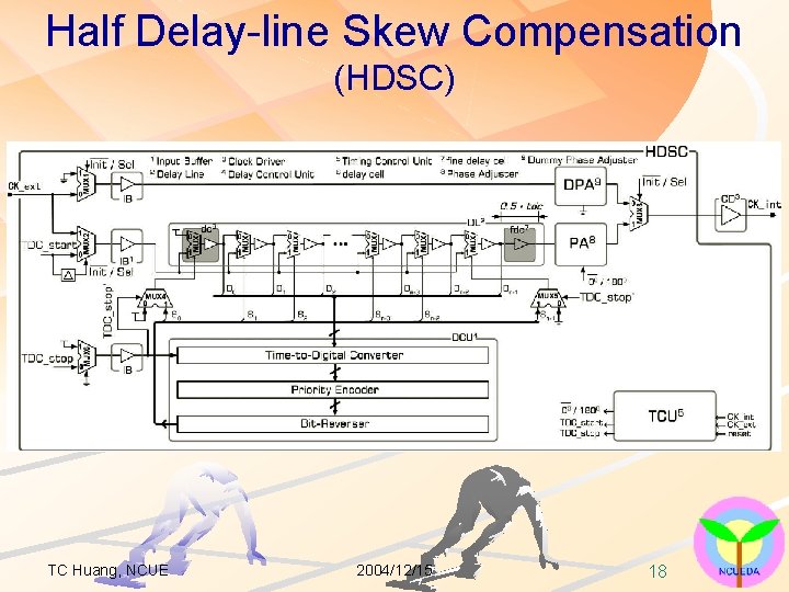
Major Previous Work • Saeki’s Digital SMD, 1996 – Only for SDRAM, with extra driver • Shim’s Analog SMD, 1999 – Accurate, high power, also 2 -cycle locking • Saeki’s Direct-skew-detect SMD, 1999 – Direct-skew-detect, also for ASIC, without extra driver, low power • Sung’s Interleaved SMD, 1999 – Double SMD circuits to use the double edges in interleaved way. • Yoo’s Open-loop Clock De-skewing Circuit, 2003 – No delay measure line, high area and power overhead due to flip-flops, difficult to matched. • Wang’s Half Delay Line Skew-Compensation – Assume duty=50%, utilizing negative edges and bit-reversing, with FFs and MUXs. . . TC Huang, NCUE 2004/12/15 10

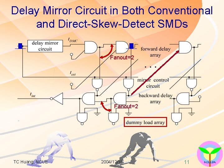
Delay Mirror Circuit in Both Conventional and Direct-Skew-Detect SMDs Fanout=2 TC Huang, NCUE 2004/12/15 11

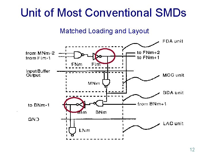
Unit of Most Conventional SMDs Matched Loading and Layout 12

Conventional SMD (SMD) Relative Resolution TC Huang, NCUE 2004/12/15 #Stages of SMD Units 13

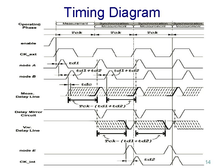
Timing Diagram 14

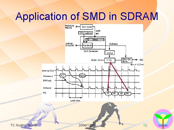
Application of SMD in SDRAM TC Huang, NCUE 2004/12/15 15

Direct-skew-detection SMD (DSMD) TC Huang, NCUE 2004/12/15 16

Interleaved SMD (ISMD) TC Huang, NCUE 2004/12/15 17

Half Delay-line Skew Compensation (HDSC) TC Huang, NCUE 2004/12/15 18

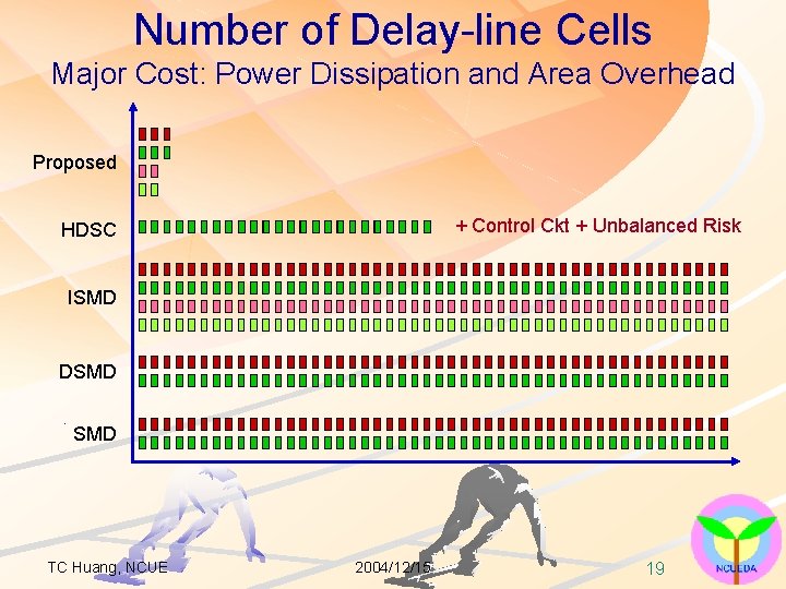
Number of Delay-line Cells Major Cost: Power Dissipation and Area Overhead Proposed + Control Ckt + Unbalanced Risk HDSC ISMD DSMD TC Huang, NCUE 2004/12/15 19

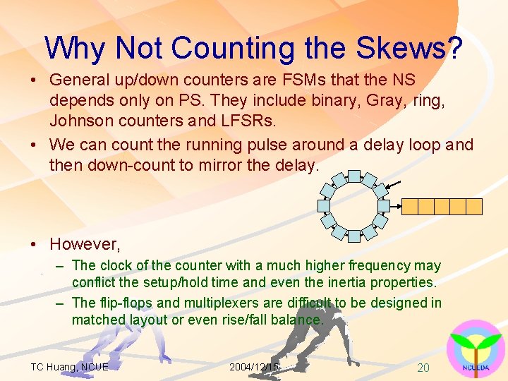
Why Not Counting the Skews? • General up/down counters are FSMs that the NS depends only on PS. They include binary, Gray, ring, Johnson counters and LFSRs. • We can count the running pulse around a delay loop and then down-count to mirror the delay. • However, – The clock of the counter with a much higher frequency may conflict the setup/hold time and even the inertia properties. – The flip-flops and multiplexers are difficult to be designed in matched layout or even rise/fall balance. TC Huang, NCUE 2004/12/15 20

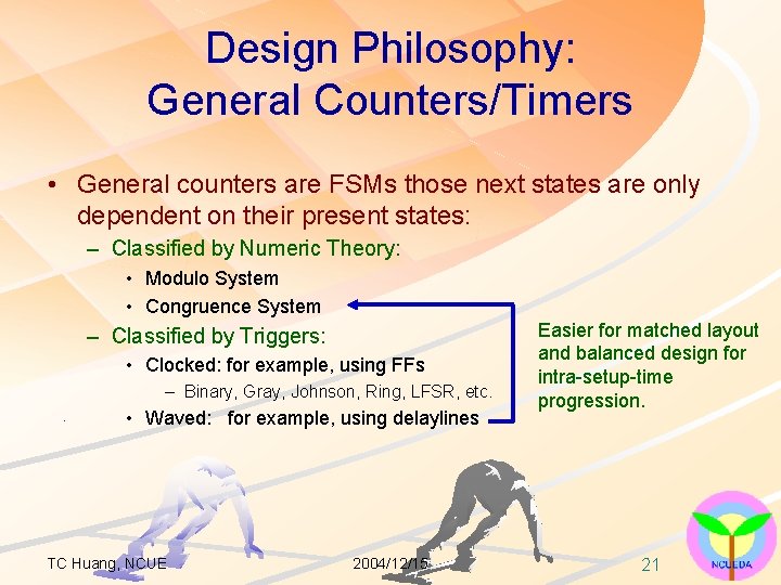
Design Philosophy: General Counters/Timers • General counters are FSMs those next states are only dependent on their present states: – Classified by Numeric Theory: • Modulo System • Congruence System – Classified by Triggers: • Clocked: for example, using FFs – Binary, Gray, Johnson, Ring, LFSR, etc. • Waved: for example, using delaylines TC Huang, NCUE 2004/12/15 Easier for matched layout and balanced design for intra-setup-time progression. 21

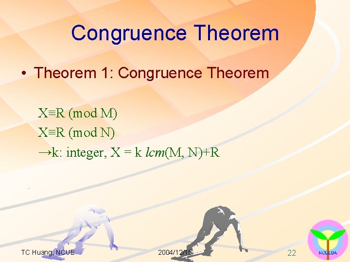
Congruence Theorem • Theorem 1: Congruence Theorem X≡R (mod M) X≡R (mod N) →k: integer, X = k lcm(M, N)+R TC Huang, NCUE 2004/12/15 22

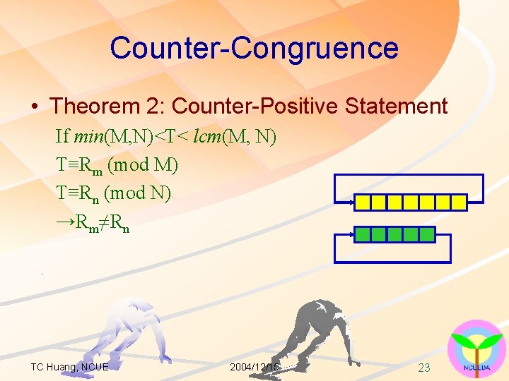
Counter-Congruence • Theorem 2: Counter-Positive Statement If min(M, N)<T< lcm(M, N) T≡Rm (mod M) T≡Rn (mod N) →Rm≠Rn TC Huang, NCUE 2004/12/15 23

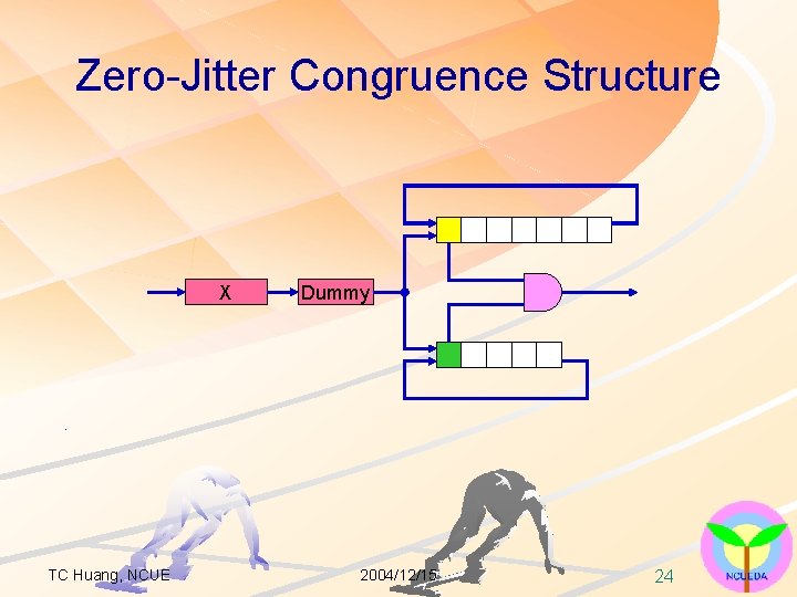
Zero-Jitter Congruence Structure X TC Huang, NCUE Dummy 2004/12/15 24

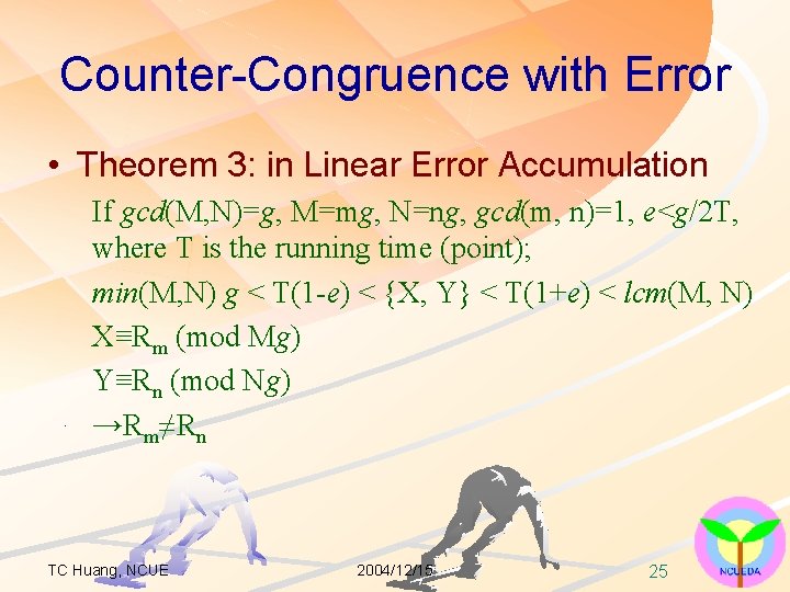
Counter-Congruence with Error • Theorem 3: in Linear Error Accumulation If gcd(M, N)=g, M=mg, N=ng, gcd(m, n)=1, e<g/2 T, where T is the running time (point); min(M, N) g < T(1 -e) < {X, Y} < T(1+e) < lcm(M, N) X≡Rm (mod Mg) Y≡Rn (mod Ng) →Rm≠Rn TC Huang, NCUE 2004/12/15 25

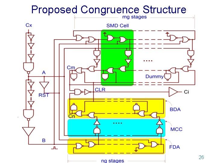
Proposed Congruence Structure 26

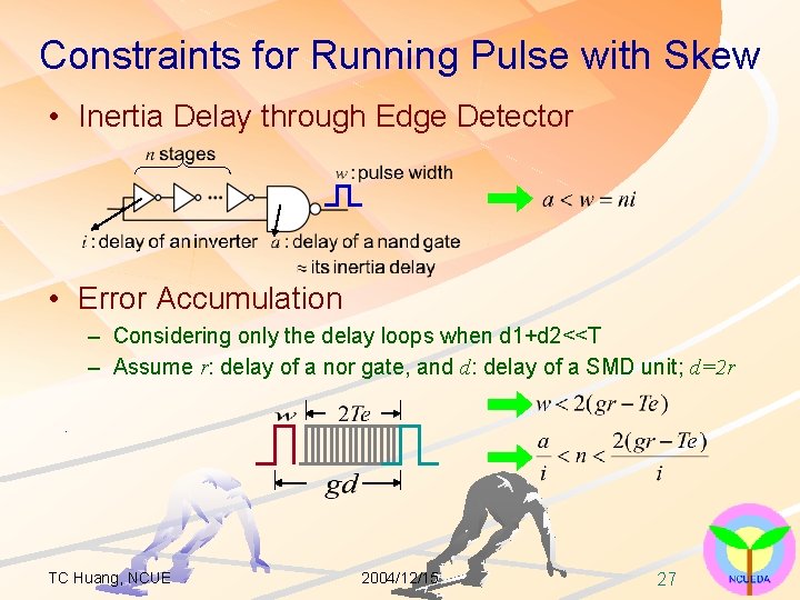
Constraints for Running Pulse with Skew • Inertia Delay through Edge Detector • Error Accumulation – Considering only the delay loops when d 1+d 2<<T – Assume r: delay of a nor gate, and d: delay of a SMD unit; d=2 r TC Huang, NCUE 2004/12/15 27

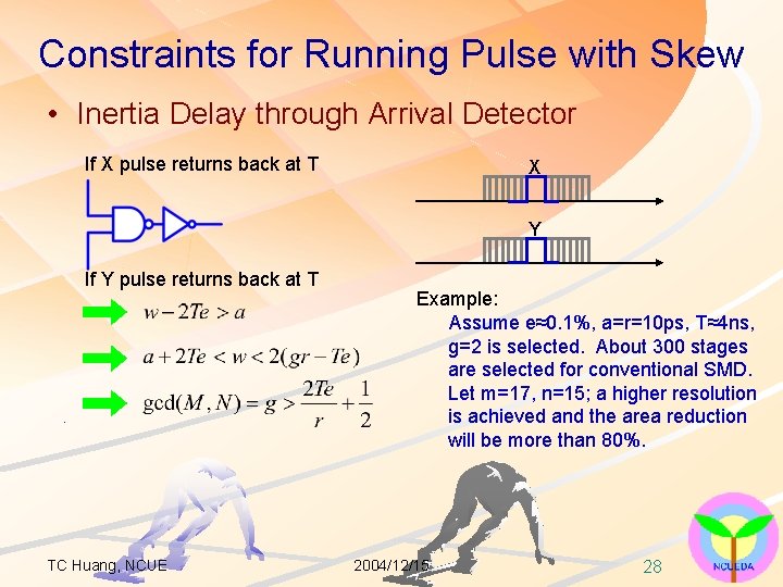
Constraints for Running Pulse with Skew • Inertia Delay through Arrival Detector If X pulse returns back at T X Y If Y pulse returns back at T TC Huang, NCUE Example: Assume e≈0. 1%, a=r=10 ps, T≈4 ns, g=2 is selected. About 300 stages are selected for conventional SMD. Let m=17, n=15; a higher resolution is achieved and the area reduction will be more than 80%. 2004/12/15 28

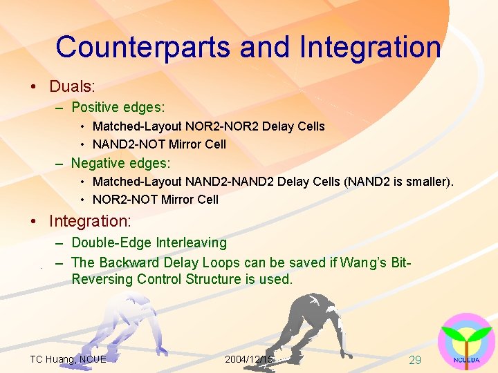
Counterparts and Integration • Duals: – Positive edges: • Matched-Layout NOR 2 -NOR 2 Delay Cells • NAND 2 -NOT Mirror Cell – Negative edges: • Matched-Layout NAND 2 -NAND 2 Delay Cells (NAND 2 is smaller). • NOR 2 -NOT Mirror Cell • Integration: – Double-Edge Interleaving – The Backward Delay Loops can be saved if Wang’s Bit. Reversing Control Structure is used. TC Huang, NCUE 2004/12/15 29

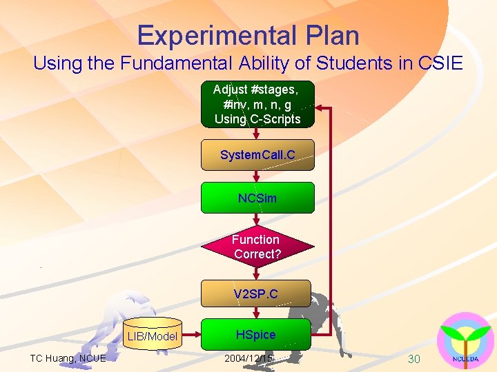
Experimental Plan Using the Fundamental Ability of Students in CSIE Adjust #stages, #inv, m, n, g Using C-Scripts System. Call. C NCSim Function Correct? V 2 SP. C LIB/Model TC Huang, NCUE HSpice 2004/12/15 30

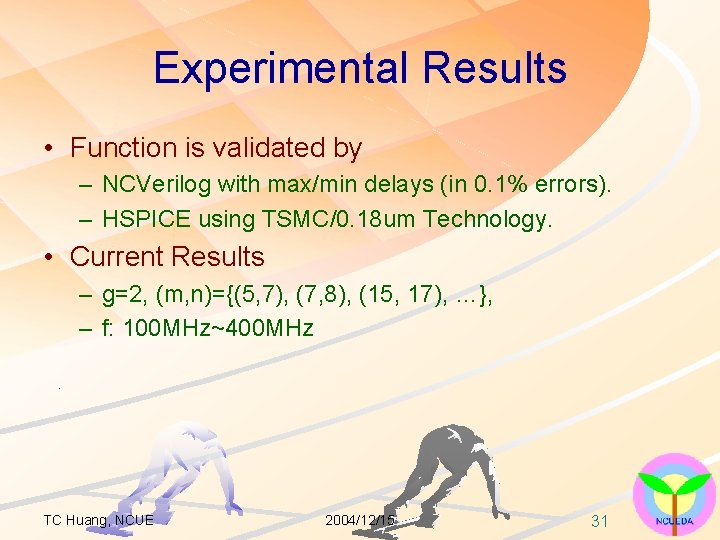
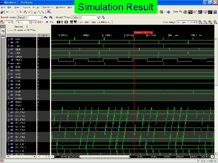
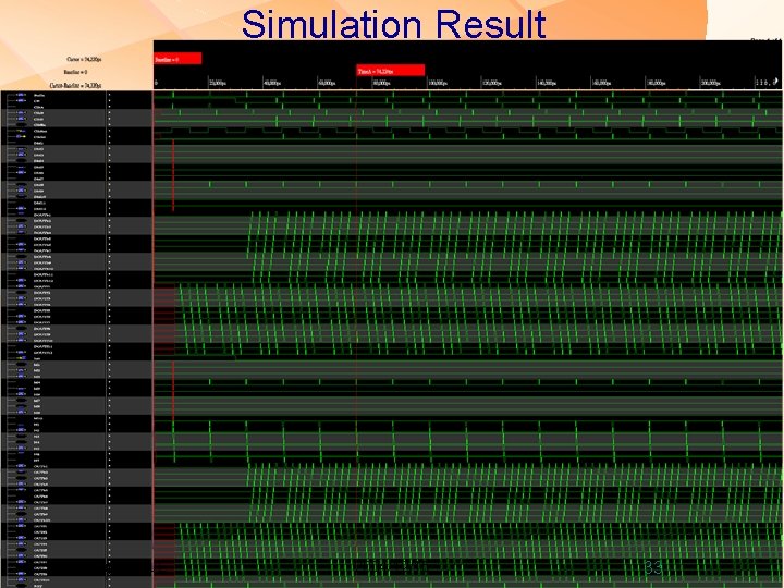
Experimental Results • Function is validated by – NCVerilog with max/min delays (in 0. 1% errors). – HSPICE using TSMC/0. 18 um Technology. • Current Results – g=2, (m, n)={(5, 7), (7, 8), (15, 17), …}, – f: 100 MHz~400 MHz TC Huang, NCUE 2004/12/15 31

Simulation Result 32

Simulation Result TC Huang, NCUE 2004/12/15 33

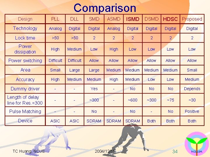
Comparison Design PLL DLL SMD ASMD ISMD DSMD HDSC Proposed Technology Analog Digital Digital Lock time >50 2 2 2 Power dissipation High Medium Low High Low Low Power switching Difficult Allow Allow Area Small Large Medium Small Accuracy High Medium Low Medium Dummy driver - - Yes - No No No Depends Length of delay line for Res. =300 - - ~300 - ~600 ~300 ~75 ~30 Pulse Matching - - No Positive Device ASIC SDRAM Both TC Huang, NCUE 2004/12/15 34

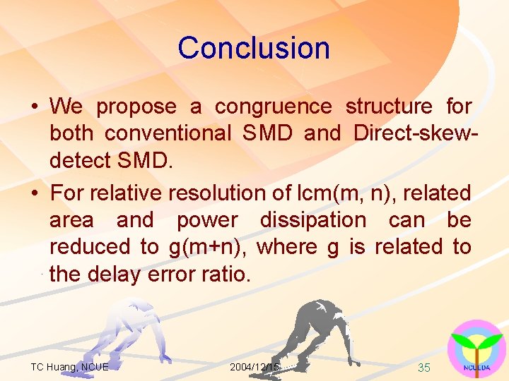
Conclusion • We propose a congruence structure for both conventional SMD and Direct-skewdetect SMD. • For relative resolution of lcm(m, n), related area and power dissipation can be reduced to g(m+n), where g is related to the delay error ratio. TC Huang, NCUE 2004/12/15 35

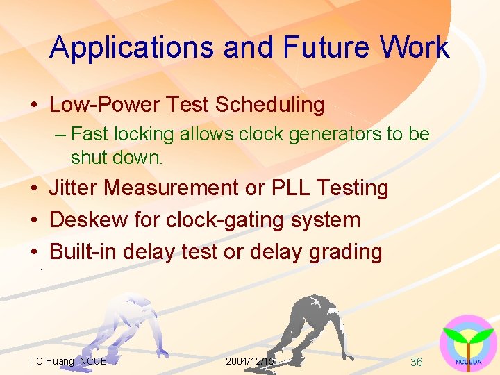
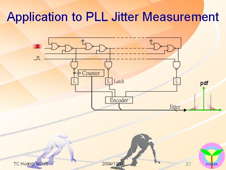
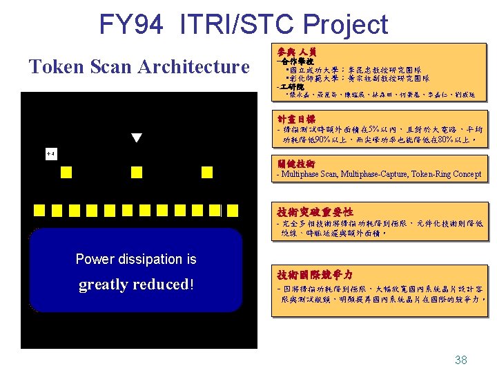
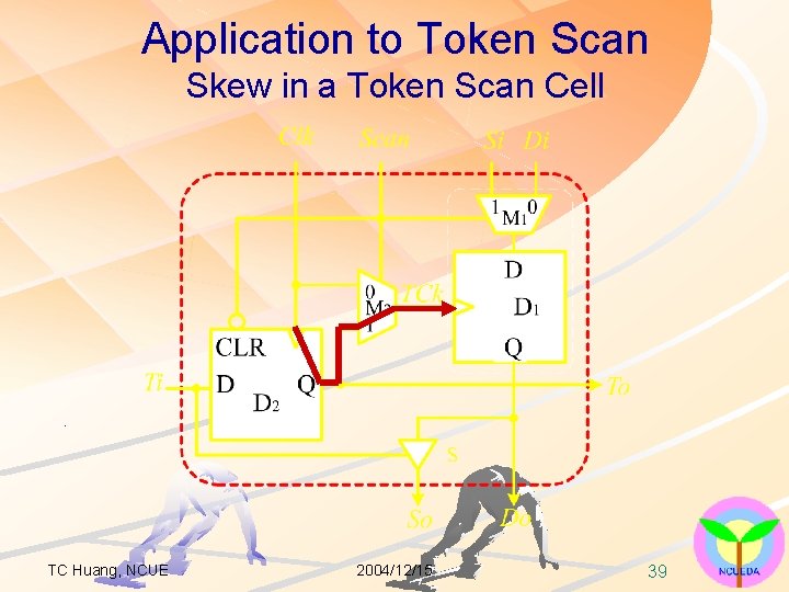
Applications and Future Work • Low-Power Test Scheduling – Fast locking allows clock generators to be shut down. • Jitter Measurement or PLL Testing • Deskew for clock-gating system • Built-in delay test or delay grading TC Huang, NCUE 2004/12/15 36

Application to PLL Jitter Measurement pdf TC Huang, NCUE 2004/12/15 37


Application to Token Scan Skew in a Token Scan Cell TC Huang, NCUE 2004/12/15 39

References 1. E. G. Friedman. Clock Distribution Networks in VLSI Circuits and Systems. Piscataway, NJ: IEEE Press, 1995. 2. J. Dunning et al. An all-digital PLL with 50 -cycle lock time suitable for high performance microprocessors. IEEE J. Solid-State Circuits, vol. 30, pp. 412 -422, Apr. 1995. 3. T. Saeki et al. A 2. 5 -ns clock access, 250 MHz, 256 -Mb SDRAM with synchronous mirror delay, IEEE J. Solid-State Circuits, vol. 30, pp. 1656 -1668, Nov. 1996. 4. T. Saeki et al. A Direct-Skew-Detect Synchronous Mirror Delay for Application-Specific Integrated Circuits. IEEE J. Solid-State Circuits, vol. 34, pp. 372 -378, Mar. 1999. 5. D. Shim et al. An Analog Synchronous Mirror Delay for High-Speed DRAM Application. IEEE J. Solid-State Circuits, vol. 34, pp. 484 -493, Apr. 1999. 6. V. Gutnik and A. P. Chandrakasan, Active GHz clock network using distributed PLL's, IEEE J. Solid-State Circuits, vol. 35, pp. 1553 -1560, Nov. 2000. 7. K. Sung et al. Low power clock generator based on area-reduced interleaved synchronous mirror delay. IEE Electronics Letters, pp. 399 -400, Vol. 38, Apr. 2002. 8. C. Yoo. An Open-Loop Clock Deskewing Circuit for High-Speed Synchronous DRAM. IEE Electronics Letters, Vol. 39, No. 1, Jan. 2003. 9. Y. -M. Wang and J. -S. Wang. A Low-Power Half-Delay-Line Fast Skew-Compensation Circuit. IEEE J. Solid-State Circuits, vol. 39, pp. 906 -918, June 2004. 10. Y. J. Yoon et al. Synchronous mirror delay for multiphase locking. IEEE Solid-State Circuits, Vol. 39, Jan. 2004 TC Huang, NCUE 2004/12/15 40

Rethink to This Innovation for CSIE Students • Basic Background on Circuit Design + Simple Numeric Concept + HDL Tools + C Scripts + Idea Ø Contributions TC Huang, NCUE 2004/12/15 41

Any Question? • • What? How? Tools? Where: – http: //163. 23. 30/tch – Email: tch@cc. ncue. edu. tw Ø Thank you for your attentions! TC Huang, NCUE 2004/12/15 42