Configuring the External memory Controller of C 6678


- Slides: 25

Configuring the External memory Controller of C 6678 – C 6670 CIV Application team July 2011 Multicore Training

Agenda 1. Short overview of the External Memory Controller (XMC) functionality 2. The MPAX registers 3. The MAR registers 4. Example 1 – Enable L 2 cache for L 2 shared memory 5. Example 2 – Disable L 1 cache for L 2 shared memory 6. Example 3 – Sharing very large DDR between multiple cores 7. Using software to configure external memory controller using CSL API 8. Implementation of Example 1 using CSL API Multicore Training

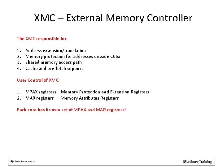
XMC – External Memory Controller The XMC responsible for: 1. 2. 3. 4. Address extension/translation Memory protection for addresses outside C 66 x Shared memory access path Cache and pre-fetch support User Control of XMC: 1. MPAX registers – Memory Protection and Extension Registers 2. MAR registers – Memory Attributes Registers Each core has its own set of MPAX and MAR registers! Multicore Training

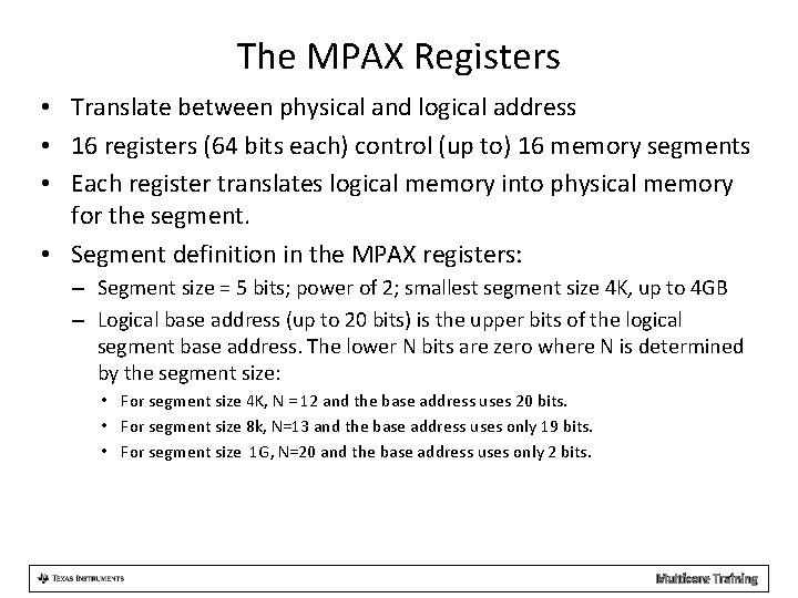
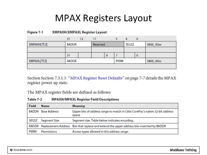
The MPAX Registers • Translate between physical and logical address • 16 registers (64 bits each) control (up to) 16 memory segments • Each register translates logical memory into physical memory for the segment. • Segment definition in the MPAX registers: – Segment size = 5 bits; power of 2; smallest segment size 4 K, up to 4 GB – Logical base address (up to 20 bits) is the upper bits of the logical segment base address. The lower N bits are zero where N is determined by the segment size: • For segment size 4 K, N = 12 and the base address uses 20 bits. • For segment size 8 k, N=13 and the base address uses only 19 bits. • For segment size 1 G, N=20 and the base address uses only 2 bits. Multicore Training

The MPAX Registers • Segment definition in the MPAX registers (continue): – Physical (replacement address) base address (up to 24 bits) is the upper bits of the physical (replacement) segment base address. The lower N bits are zero where N is determined by the segment size: • For segment size 4 K, N = 12 and the base address uses up to 24 bits. • For segment size 8 k, N=13 and the base address uses up to 23 bits. • For segment size 1 G, N=20 and the base address uses up to 6 bits. – Permission types allowed in this address range: • Three bits are dedicated for supervisor mode (write, read, execute) • Three bits are dedicated for user mode (write, read, execute) Multicore Training

MPAX Registers Layout Multicore Training

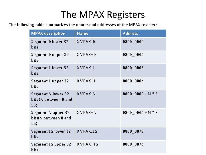
The MPAX Registers The following table summarizes the names and addresses of the MPAX registers: MPAX description Name Address Segment 0 lower 32 bits XMPAXL 0 0800_0000 Segment 0 upper 32 bits XMPAXH 0 0800_0004 Segment 1 lower 32 bits XMPAXL 1 0800_0008 Segment 1 upper 32 bits XMPAXH 1 0800_000 c Segment N lower 32 bits (N between 0 and 15) XMPAXLN 0800_0000 + N * 8 Segment N upper 32 bits(N between 0 and 15) XMPAXHN 0800_0004 + N * 8 Segment 15 lower 32 bits XMPAXL 15 0800_0078 Segment 15 upper 32 bits XMPAXH 15 0800_007 c Multicore Training

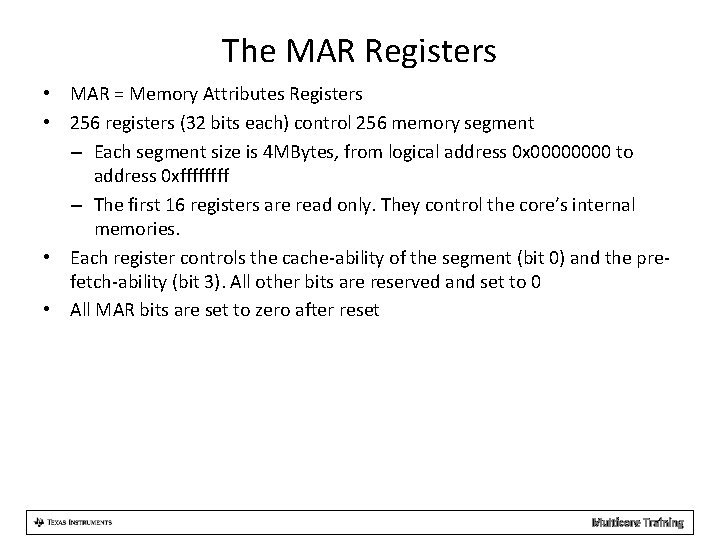
The MAR Registers • MAR = Memory Attributes Registers • 256 registers (32 bits each) control 256 memory segment – Each segment size is 4 MBytes, from logical address 0 x 0000 to address 0 xffff – The first 16 registers are read only. They control the core’s internal memories. • Each register controls the cache-ability of the segment (bit 0) and the prefetch-ability (bit 3). All other bits are reserved and set to 0 • All MAR bits are set to zero after reset Multicore Training

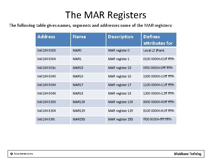
The MAR Registers The following table gives names, segments and addresses some of the MAR registers: Address Name Description Defines attributes for 0 x 0184 8000 MAR register 0 Local L 2 (Ram) 0 x 0184 8004 MAR 1 MAR register 1 0100 0000 h-01 ff ffffh 0 x 0184 803 c MAR 15 MAR register 15 0 f 00 0000 h-0 fff ffffh 0 x 0184 8040 MAR 16 MAR register 16 1000 0000 h-10 ff ffffh 0 x 0184 8044 MAR 17 MAR register 17 1100 0000 h-11 ff ffffh 0 x 0184 8048 MAR 18 MAR register 18 1200 0000 h-12 ff ffffh 0 x 0184 8200 MAR 128 MAR register 128 8000 0000 h-80 ff ffffh 0 x 0184 8204 MAR 129 MAR register 129 8100 0000 h-81 ff ffffh 0 x 0184 83 fc MAR 255 MAR register 255 ff 00 0000 h-ffffh Multicore Training

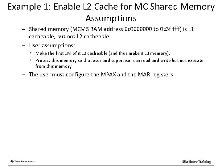
Example 1: Enable L 2 Cache for MC Shared Memory Assumptions – Shared memory (MCMS RAM address 0 c 0000000 to 0 c 3 f ffff) is L 1 cacheable, but not L 2 cacheable. – User assumptions: • Make the first 1 M of it L 2 cacheable (and thus make it L 3 memory). • Protect this memory so that user and supervisor can read and write but not execute from this memory – The user must configure the MPAX and the MAR registers. Multicore Training

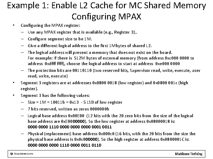
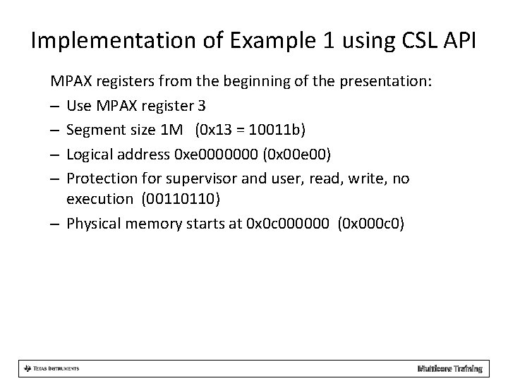
Example 1: Enable L 2 Cache for MC Shared Memory Configuring MPAX • • • Configuring the MPAX register: – Use any MPAX register that is available (e. g. , Register 3). . – Configure segment size to be 1 M. – Give a different logical address to the first 1 Mbytes of shared L 2. – The logical address will present a memory that does not exist on the board. For example: If there is 512 M bytes of external memory (from address 0 xc 0000 to address 0 xdfff ffff), choose the logical address to start at address 0 xe 0000 – The protection bits are 00110110 (two reserved bits, Supervisor read, write, execute, user read, write, execute) Segment 3 registers are at addresses 0 x 0800 0018 (low register) and 0 x 0800 001 c (high register). Segment 3 has the following values: – Size = 1 M = 10011 b = 0 x 13 - 5 LSB of low register – 7 bits reserved, written as zeros 0000000 b – Logical base address 0 x 00 E 00 (12 bits with the 20 zero bits from the size of the logical base address are 0 x. E 0000000). So the low register at address 0 x 08000018 is: 0000 1110 0000 0001 0011 – Physical (replacement) base address 0 x 000 c 0 (16 bits, with the 20 bits from the size the physical base address is 0 x 0 c 000000). So the high register at address 0 x 0800001 C is: 0000 1110 0000 0011 0110 Multicore Training

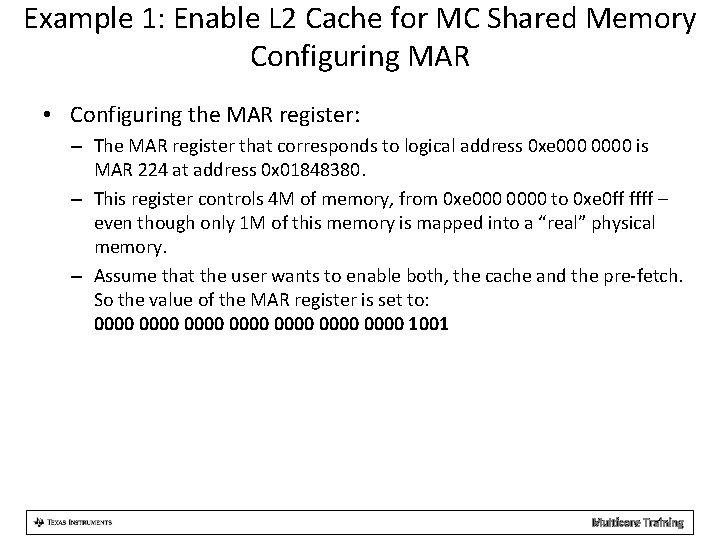
Example 1: Enable L 2 Cache for MC Shared Memory Configuring MAR • Configuring the MAR register: – The MAR register that corresponds to logical address 0 xe 0000 is MAR 224 at address 0 x 01848380. – This register controls 4 M of memory, from 0 xe 0000 to 0 xe 0 ff ffff – even though only 1 M of this memory is mapped into a “real” physical memory. – Assume that the user wants to enable both, the cache and the pre-fetch. So the value of the MAR register is set to: 0000 0000 1001 Multicore Training

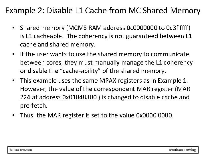
Example 2: Disable L 1 Cache from MC Shared Memory • Shared memory (MCMS RAM address 0 c 0000000 to 0 c 3 f ffff) is L 1 cacheable. The coherency is not guaranteed between L 1 cache and shared memory. • If the user wants to use the shared memory to communicate between cores, they must manually manage the L 1 coherency or disable the “cache-ability” of the shared memory. • This example uses the same MPAX registers as in Example 1. However, the value of the correspondent MAR register (MAR 224 at address 0 x 01848380 ) is changed to disable cache and pre-fetch. • Thus, the MAR register is set to the value 0 x 0000. Multicore Training

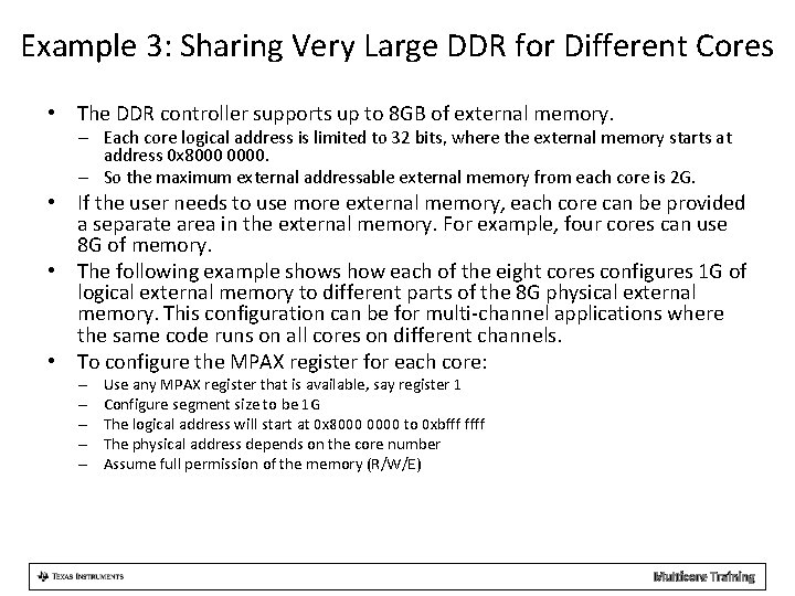
Example 3: Sharing Very Large DDR for Different Cores • The DDR controller supports up to 8 GB of external memory. – Each core logical address is limited to 32 bits, where the external memory starts at address 0 x 8000 0000. – So the maximum external addressable external memory from each core is 2 G. • If the user needs to use more external memory, each core can be provided a separate area in the external memory. For example, four cores can use 8 G of memory. • The following example shows how each of the eight cores configures 1 G of logical external memory to different parts of the 8 G physical external memory. This configuration can be for multi-channel applications where the same code runs on all cores on different channels. • To configure the MPAX register for each core: – – – Use any MPAX register that is available, say register 1 Configure segment size to be 1 G The logical address will start at 0 x 8000 0000 to 0 xbfff ffff The physical address depends on the core number Assume full permission of the memory (R/W/E) Multicore Training

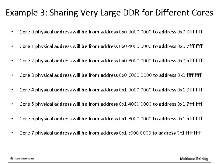
Example 3: Sharing Very Large DDR for Different Cores • Core 0 physical address will be from address 0 x 0 0000 to address 0 x 0 3 fff ffff • Core 1 physical address will be from address 0 x 0 4000 0000 to address 0 x 0 7 fff ffff • Core 2 physical address will be from address 0 x 0 8000 0000 to address 0 x 0 bfff ffff • Core 3 physical address will be from address 0 x 0 C 0000 to address 0 x 0 ffff • Core 4 physical address will be from address 0 x 1 0000 to address 0 x 1 3 fff ffff • Core 5 physical address will be from address 0 x 1 4000 0000 to address 0 x 1 7 fff ffff • Core 6 physical address will be from address 0 x 1 8000 0000 to address 0 x 1 bfff ffff • Core 7 physical address will be from address 0 x 1 c 0000 to address 0 x 1 ffff Multicore Training

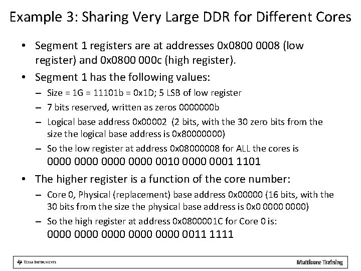
Example 3: Sharing Very Large DDR for Different Cores • Segment 1 registers are at addresses 0 x 0800 0008 (low register) and 0 x 0800 000 c (high register). • Segment 1 has the following values: – Size = 1 G = 11101 b = 0 x 1 D; 5 LSB of low register – 7 bits reserved, written as zeros 0000000 b – Logical base address 0 x 00002 (2 bits, with the 30 zero bits from the size the logical base address is 0 x 80000000) – So the low register at address 0 x 08000008 for ALL the cores is 0000 0010 0001 1101 • The higher register is a function of the core number: – Core 0, Physical (replacement) base address 0 x 00000 (16 bits, with the 30 bits from the size the physical base address is 0 x 0 0000) – So the high register at address 0 x 0800001 C for Core 0 is: 0000 0000 0011 1111 Multicore Training

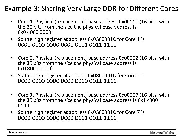
Example 3: Sharing Very Large DDR for Different Cores • Core 1, Physical (replacement) base address 0 x 00001 (16 bits, with the 30 bits from the size the physical base address is 0 x 0 4000 0000) • So the high register at address 0 x 0800001 C for Core 1 is 0000 0001 0011 1111 • Core 2, Physical (replacement) base address 0 x 00002 (16 bits, with the 30 bits from the size the physical base address is 0 x 0 8000 0000) • So the high register at address 0 x 0800001 C for Core 2 is 0000 0010 0011 1111 • Core 7, Physical (replacement) base address 0 x 00007 (16 bits, with the 30 bits from the size the physical base address is 0 x 1 c 0000) • So the high register at address 0 x 0800001 C for Core 7 is 0000 0111 0011 1111 Multicore Training

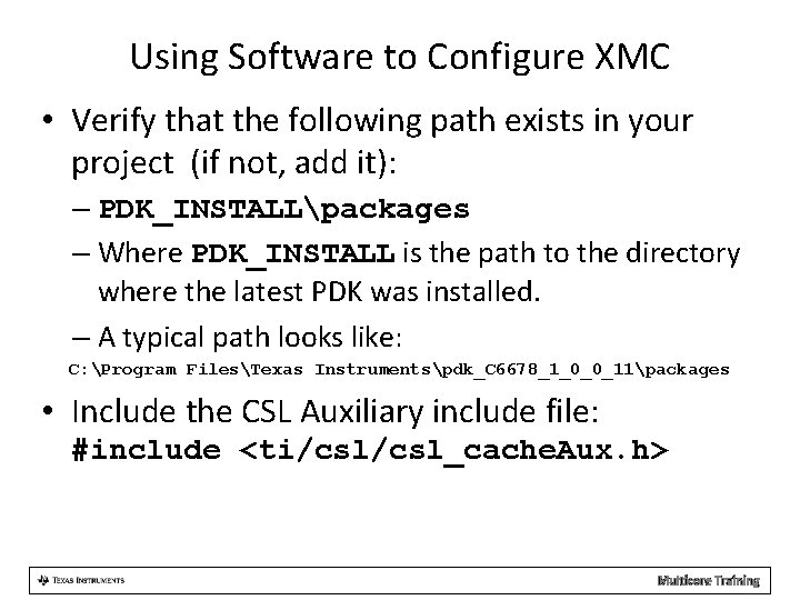
Using Software to Configure XMC • Verify that the following path exists in your project (if not, add it): – PDK_INSTALLpackages – Where PDK_INSTALL is the path to the directory where the latest PDK was installed. – A typical path looks like: C: Program FilesTexas Instrumentspdk_C 6678_1_0_0_11packages • Include the CSL Auxiliary include file: #include <ti/csl_cache. Aux. h> Multicore Training

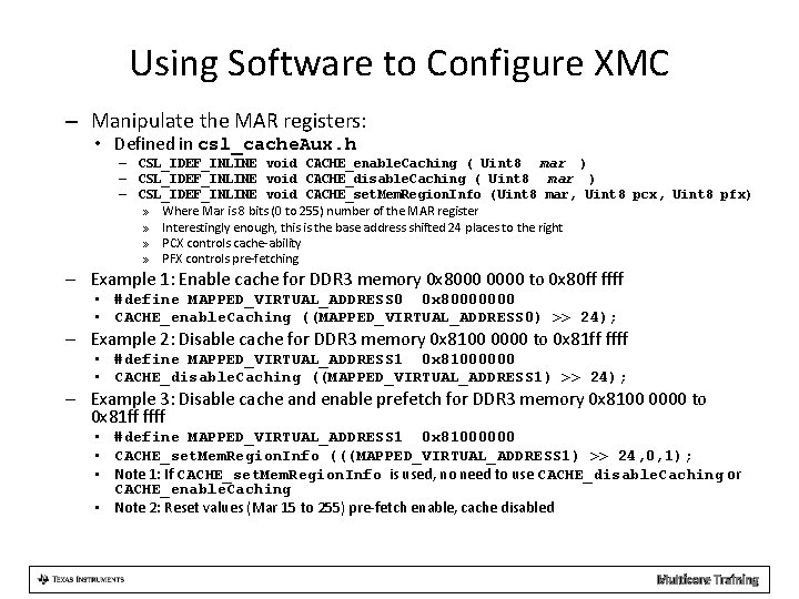
Using Software to Configure XMC – Manipulate the MAR registers: • Defined in csl_cache. Aux. h – CSL_IDEF_INLINE void CACHE_enable. Caching ( Uint 8 mar ) – CSL_IDEF_INLINE void CACHE_disable. Caching ( Uint 8 mar ) – CSL_IDEF_INLINE void CACHE_set. Mem. Region. Info (Uint 8 mar, Uint 8 pcx, Uint 8 pfx) » Where Mar is 8 bits (0 to 255) number of the MAR register » Interestingly enough, this is the base address shifted 24 places to the right » PCX controls cache-ability » PFX controls pre-fetching – Example 1: Enable cache for DDR 3 memory 0 x 8000 0000 to 0 x 80 ff ffff • #define MAPPED_VIRTUAL_ADDRESS 0 0 x 80000000 • CACHE_enable. Caching ((MAPPED_VIRTUAL_ADDRESS 0) >> 24); – Example 2: Disable cache for DDR 3 memory 0 x 8100 0000 to 0 x 81 ff ffff • #define MAPPED_VIRTUAL_ADDRESS 1 0 x 81000000 • CACHE_disable. Caching ((MAPPED_VIRTUAL_ADDRESS 1) >> 24); – Example 3: Disable cache and enable prefetch for DDR 3 memory 0 x 8100 0000 to 0 x 81 ff ffff • #define MAPPED_VIRTUAL_ADDRESS 1 0 x 81000000 • CACHE_set. Mem. Region. Info (((MAPPED_VIRTUAL_ADDRESS 1) >> 24, 0, 1); • Note 1: If CACHE_set. Mem. Region. Info is used, no need to use CACHE_disable. Caching or CACHE_enable. Caching • Note 2: Reset values (Mar 15 to 255) pre-fetch enable, cache disabled Multicore Training

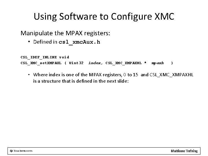
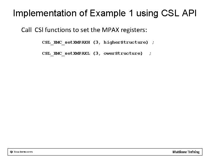
Using Software to Configure XMC Manipulate the MPAX registers: • Defined in csl_xmc. Aux. h CSL_IDEF_INLINE void CSL_XMC_set. XMPAXL ( Uint 32 index, CSL_XMC_XMPAXHL * mpaxh ) • Where index is one of the MPAX registers, 0 to 15 and CSL_XMC_XMPAXHL is a structure that is defined in the next slide: Multicore Training

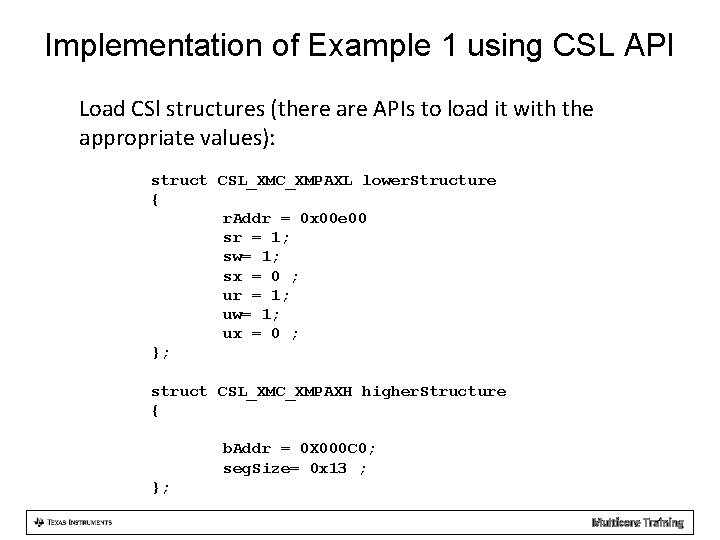
Definition: CSL_XMC_XMPAXL typedef struct CSL_XMC_XMPAXL { /** Replacement Address */ Uint 32 r. Addr; /** When set, supervisor may read from segment */ Uint 32 sr; /** When set, supervisor may write to segment */ Uint 32 sw; /** When set, supervisor may execute from segment */ Uint 32 sx; /** When set, user may read from segment */ Uint 32 ur; /** When set, user may write to segment */ Uint 32 uw; /** When set, user may execute from segment */ Uint 32 ux; }CSL_XMC_XMPAXL; Multicore Training

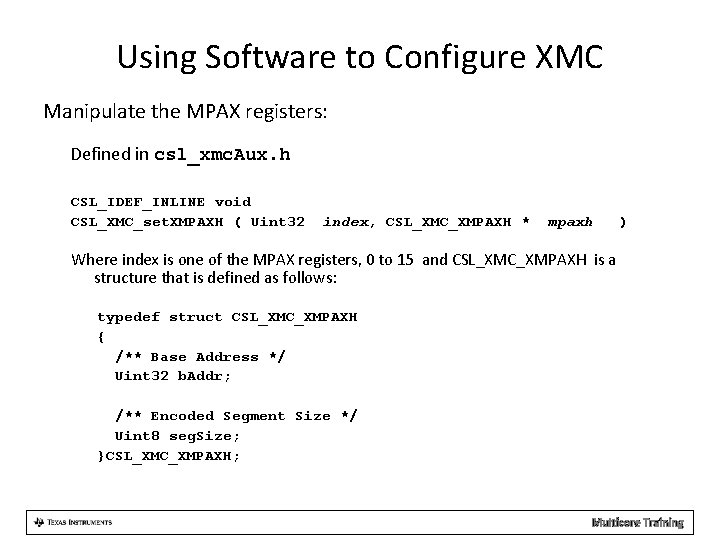
Using Software to Configure XMC Manipulate the MPAX registers: Defined in csl_xmc. Aux. h CSL_IDEF_INLINE void CSL_XMC_set. XMPAXH ( Uint 32 index, CSL_XMC_XMPAXH * mpaxh ) Where index is one of the MPAX registers, 0 to 15 and CSL_XMC_XMPAXH is a structure that is defined as follows: typedef struct CSL_XMC_XMPAXH { /** Base Address */ Uint 32 b. Addr; /** Encoded Segment Size */ Uint 8 seg. Size; }CSL_XMC_XMPAXH; Multicore Training

Implementation of Example 1 using CSL API MPAX registers from the beginning of the presentation: – Use MPAX register 3 – Segment size 1 M (0 x 13 = 10011 b) – Logical address 0 xe 0000000 (0 x 00 e 00) – Protection for supervisor and user, read, write, no execution (00110110) – Physical memory starts at 0 x 0 c 000000 (0 x 000 c 0) Multicore Training

Implementation of Example 1 using CSL API Load CSl structures (there are APIs to load it with the appropriate values): struct CSL_XMC_XMPAXL lower. Structure { r. Addr = 0 x 00 e 00 sr = 1; sw= 1; sx = 0 ; ur = 1; uw= 1; ux = 0 ; }; struct CSL_XMC_XMPAXH higher. Structure { b. Addr = 0 X 000 C 0; seg. Size= 0 x 13 ; }; Multicore Training

Implementation of Example 1 using CSL API Call CSl functions to set the MPAX registers: CSL_XMC_set. XMPAXH (3, higher. Structure) ; CSL_XMC_set. XMPAXL (3, ower. Structure) ; Multicore Training