
Confidential Material MAX 10 FPGAs Overview Tom Schulte
- Slides: 20
Confidential Material MAX 10 FPGAs - Overview Tom Schulte Low Cost Product Marketing 5/9/2014
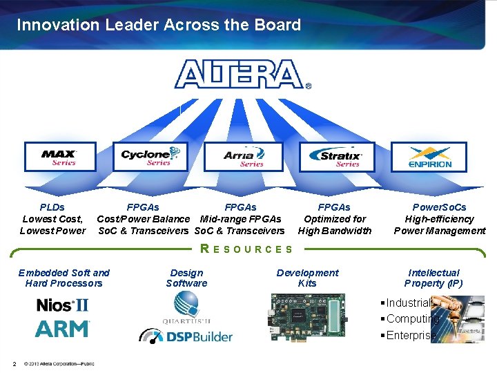
Innovation Leader Across the Board PLDs Lowest Cost, Lowest Power FPGAs Cost/Power Balance Mid-range FPGAs So. C & Transceivers R Embedded Soft and Hard Processors Design Software FPGAs Optimized for High Bandwidth Power. So. Cs High-efficiency Power Management ESOURCES Development Kits Intellectual Property (IP) § Industrial § Computing § Enterprise 2
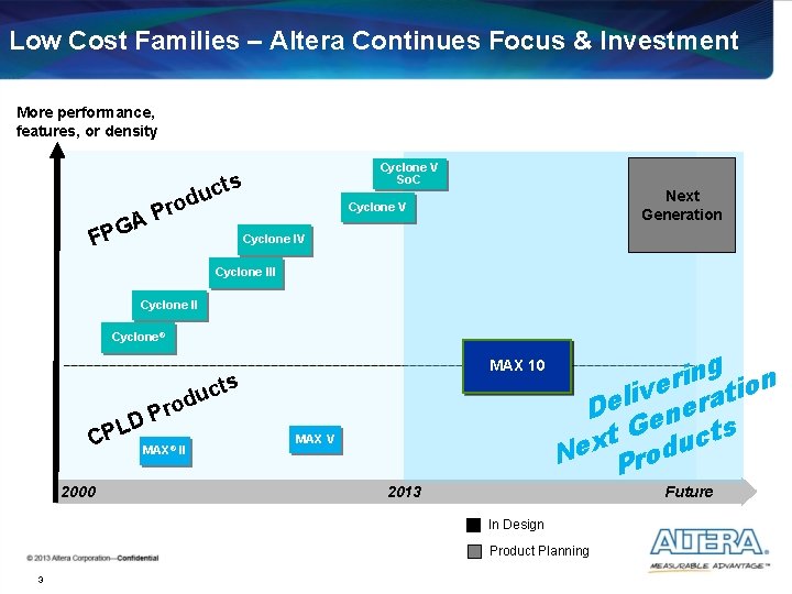
Low Cost Families – Altera Continues Focus & Investment More performance, features, or density Cyclone V So. C s t c u od r P GA FP Next Generation Cyclone V Cyclone III Cyclone® MAX 10 s uct d ro P D L CP 2000 MAX® II MAX V 2013 g n i r n e o i v t i Del enera s G t t c x Ne Produ Future In Design Product Planning 3
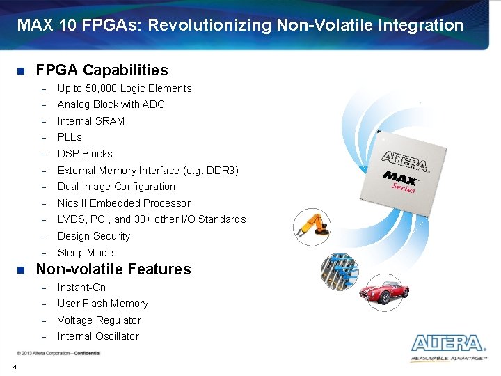
MAX 10 FPGAs: Revolutionizing Non-Volatile Integration n n 4 FPGA Capabilities - Up to 50, 000 Logic Elements - Analog Block with ADC - Internal SRAM - PLLs - DSP Blocks - External Memory Interface (e. g. DDR 3) - Dual Image Configuration - Nios II Embedded Processor - LVDS, PCI, and 30+ other I/O Standards - Design Security - Sleep Mode Non-volatile Features - Instant-On - User Flash Memory - Voltage Regulator - Internal Oscillator
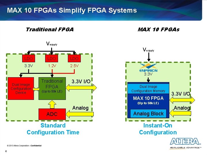
MAX 10 FPGAs Simplify FPGA Systems Traditional FPGA MAX 10 FPGAs Vsupply LDO LDO 3. 3 V 1. 2 V 2. 5 V 3. 3 V Dual Image Configuration Device Traditional FPGA 3. 3 V I/O Dual Image Configuration Memory (Up to 50 k LE) MAX 10 FPGA 3. 3 V I/O (Up to 50 k LE) Analog ADC Standard Configuration Time 5 Analog Block Instant-On Configuration
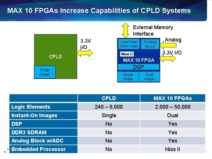
MAX 10 FPGAs Increase Capabilities of CPLD Systems External Memory Interface Analog User Flash 3. 3 V I/O (Nios code) 3. 3 V I/O CPLD MAX 10 FPGA DSP Single Image Dual Image CPLD MAX 10 FPGAs 240 – 8, 000 2, 000 – 50, 000 Single Dual DSP No Yes DDR 3 SDRAM No Yes Analog Block w/ADC No Yes Embedded Processor No Nios II Logic Elements Instant-On Images 6 Block
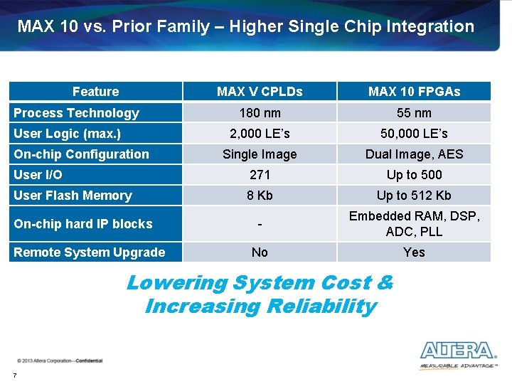
MAX 10 vs. Prior Family – Higher Single Chip Integration Feature MAX V CPLDs MAX 10 FPGAs 180 nm 55 nm 2, 000 LE’s 50, 000 LE’s Single Image Dual Image, AES User I/O 271 Up to 500 User Flash Memory 8 Kb Up to 512 Kb - Embedded RAM, DSP, ADC, PLL No Yes Process Technology User Logic (max. ) On-chip Configuration On-chip hard IP blocks Remote System Upgrade Lowering System Cost & Increasing Reliability 7
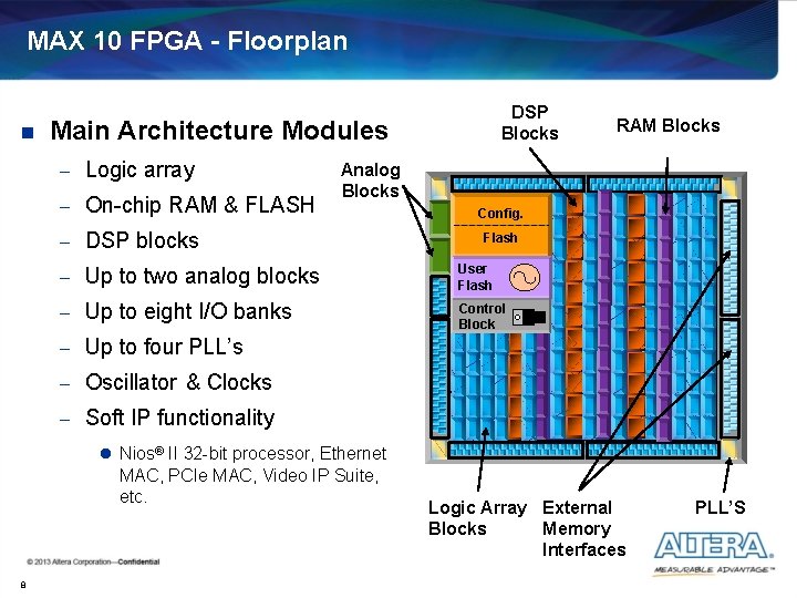
MAX 10 FPGA - Floorplan n DSP Blocks Main Architecture Modules - Logic array - On-chip RAM & FLASH RAM Blocks Analog Blocks - DSP blocks Config. Flash - Up to two analog blocks User Flash - Up to eight I/O banks Control Block - Up to four PLL’s - Oscillator & Clocks - Soft IP functionality l Nios® II 32 -bit processor, Ethernet MAC, PCIe MAC, Video IP Suite, etc. 8 Logic Array External Blocks Memory Interfaces PLL’S
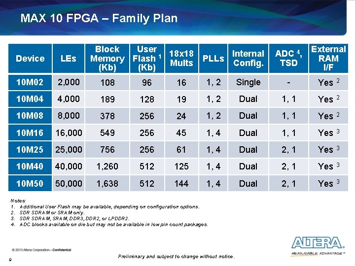
MAX 10 FPGA – Family Plan Block User 18 x 18 Internal Memory Flash 1 PLLs Mults Config. (Kb) External RAM I/F Device LEs 10 M 02 2, 000 108 96 16 1, 2 Single - Yes 2 10 M 04 4, 000 189 128 19 1, 2 Dual 1, 1 Yes 2 10 M 08 8, 000 378 256 24 1, 2 Dual 1, 1 Yes 2 10 M 16 16, 000 549 256 45 1, 4 Dual 1, 1 Yes 3 10 M 25 25, 000 756 256 61 1, 4 Dual 2, 1 Yes 3 10 M 40 40, 000 1, 260 512 125 1, 4 Dual 2, 1 Yes 3 10 M 50 50, 000 1, 638 512 144 1, 4 Dual 2, 1 Yes 3 Notes: 1. Additional User Flash may be available, depending on configuration options. 2. SDRAM or SRAM only. 3. SDRAM, SRAM, DDR 3, DDR 2, or LPDDR 2. 4. ADC blocks available on die but may not be available in low pin count packages. 9 ADC 4, TSD Preliminary and subject to change without notice.
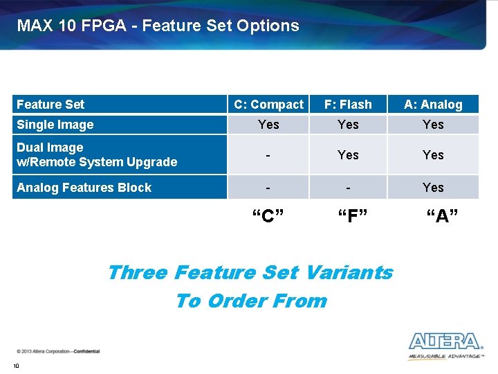
MAX 10 FPGA - Feature Set Options Feature Set C: Compact F: Flash A: Analog Yes Yes Dual Image w/Remote System Upgrade - Yes Analog Features Block - - Yes Single Image “C” “F” Three Feature Set Variants To Order From 10 “A”
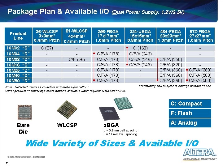
Package Plan & Available I/O (Dual Power Supply: 1. 2 V/2. 5 V) Product Line 10 M 02 10 M 04 10 M 08 10 M 16 10 M 25 10 M 40 10 M 50 “D” “D” 81 -WLCSP 36 -WLCSP 2 3 x 3 mm 4 x 4 mm 2 0. 4 mm Pitch C (27) - C/F (56) - 256 -FBGA 17 x 17 mm 2 1. 0 mm Pitch 324 -UBGA 15 x 15 mm 2 0. 8 mm Pitch C/F/A (178) C/F/A (178) C (160) C/F/A (246) - Note: Selected items = Pro-active automotive p/n rollout. Other product line/package combinations available upon request & sufficient ROI. 484 -FBGA 672 -FBGA 2 23 x 23 mm 27 x 27 mm 2 1. 0 mm Pitch C/F/A (250) C/F/A (320) C/F/A (360) C/F/A (380) C/F/A (500) Preliminary and subject to change without notice C: Compact F: Flash Bare Die WLCSP x. BGA A: Analog U = 0. 8 mm ball spacing F = 1. 0 mm ball spacing Wide Variety of Sizes & Available I/O 11
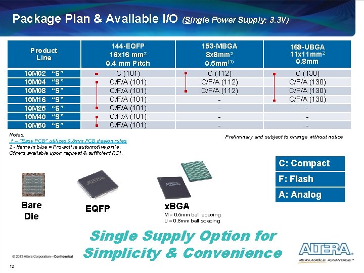
Package Plan & Available I/O (Single Power Supply: 3. 3 V) Product Line 10 M 02 10 M 04 10 M 08 10 M 16 10 M 25 10 M 40 10 M 50 “S” “S” 144 -EQFP 16 x 16 mm 2 0. 4 mm Pitch C (101) C/F/A (101) C/F/A (101) 153 -MBGA 8 x 8 mm 2 0. 5 mm(1) C (112) C/F/A (112) - Notes: 1 – “Easy PCB” utilizes 0. 8 mm PCB design rules 2 - Items in blue = Pro-active automotive p/n’s. Others available upon request & sufficient ROI. 169 -UBGA 11 x 11 mm 2 0. 8 mm C (130) C/F/A (130) - Preliminary and subject to change without notice C: Compact F: Flash A: Analog Bare Die EQFP x. BGA M = 0. 5 mm ball spacing U = 0. 8 mm ball spacing Single Supply Option for Simplicity & Convenience 12
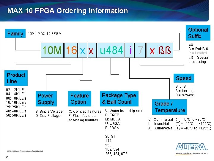
MAX 10 FPGA Ordering Information Family Optional Suffix 10 M: MAX 10 FPGA ES G = Ro. HS 6 P = Leaded ßß = Special processing 10 M 16 x x u 484 i 7 x ßß Product Line 02: 2 K LE’s 04: 4 K LE’s 08: 8 K LE’s 16: 16 K LE’s 25: 25 K LE’s 40: 40 K LE’s 50: 50 K LE’s Speed Power Supply S: Single Voltage D: Dual Voltage Feature Option C: Compact features F: Flash features A: Analog features Package Type & Ball Count V: Wafer level chip-scale E: EQFP M: MBGA U: UBGA F: FBGA 36, 81 144 153 169, 324 256, 484, 672 13 6, 7, 8 6 = fastest, 8 = slowest Grade / Temperature C: Commercial (TJ = 0°C to +85°C) I: Industrial (T J = -40°C to +100°C) A: Automotive (TJ = -40°C to +125°C)
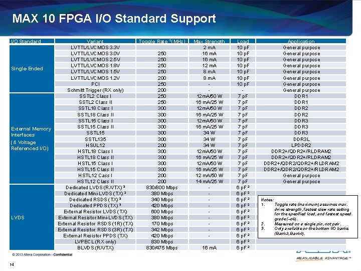
MAX 10 FPGA I/O Standard Support I/O Standard Single-Ended External Memory Interfaces (& Voltage Referenced I/O) LVDS 14 Variant LVTTL/LVCMOS 3. 3 V LVTTL/LVCMOS 3. 0 V LVTTL/LVCMOS 2. 5 V LVTTL/LVCMOS 1. 8 V LVTTL/LVCMOS 1. 5 V LVTTL/LVCMOS 1. 2 V PCI Schmitt Trigger (RX only) SSTL 2 Class II SSTL 18 Class II SSTL 15 SSTL 135 HSUL 12 HSTL 18 Class II HSTL 15 Class II HSTL 12 Cass I HSTL 12 Class II Dedicated LVDS (RX/TX) 3 Dedicated Mini-LVDS (TX) 3 Dedicated RSDS (TX) 3 Dedicated PPDS (TX) 3 External Resistor LVDS (TX) External Resistor Mini-LVDS (TX) External Resistor RSDS (1 R) (TX) External Resistor RSDS (3 R) (TX) External Resistor PPDS (TX) LVPECL (RX only) BLVDS (RX/TX) Toggle Rate 1 (MHz) 250 250 200 250 250 300 300 300 200 830/800 Mbps 380 Mbps 340 Mbps 420 Mbps 600 Mbps 380 Mbps 170 Mbps 342 Mbps 420 Mbps 830/475 Mbps Max Strength 2 m. A 16 m. A 12 m. A 8 m. A 12 m. A/50 W 16 m. A/25 W 34 W 12 m. A/50 W 16 m. A/25 W 12 m. A/50 W 14 m. A/25 W 16 m. A Load 10 p. F 10 p. F 7 p. F 6 p. F 2 6 p. F 2 Application General purpose General purpose DDR 1 DDR 2 DDR 3 L LPDDR 2+/QDR 2+/RLDRAM 2 DDR 2+/QDR 2/QDR 2+/RLDRAM 2 General purpose Notes: 1. Toggle rate (maximum) assumes max. drive strength, fastest slew rate setting for the specified load, and fastest speed grade (–c 6). 2. Measured on a single pin, not pair. 3. Only available on the bottom I/O banks (Bank 3, Bank 4).
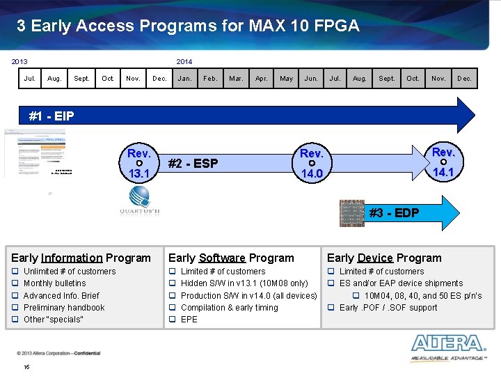
3 Early Access Programs for MAX 10 FPGA 2013 2014 Jul. Aug. Sept. Oct. Nov. Dec. Jan. Feb. Mar. Apr. May Jun. Jul. Aug. Sept. Oct. Nov. Dec. #1 - EIP Rev. MAX 10 FPGA Device Handbook 13. 1 #2 - ESP Rev. 14. 0 14. 1 #3 - EDP Early Information Program Early Software Program Early Device Program q q q Limited # of customers q ES and/or EAP device shipments q 10 M 04, 08, 40, and 50 ES p/n’s q Early. POF /. SOF support Unlimited # of customers Monthly bulletins Advanced Info. Brief Preliminary handbook Other “specials” 15 Limited # of customers Hidden S/W in v 13. 1 (10 M 08 only) Production S/W in v 14. 0 (all devices) Compilation & early timing EPE
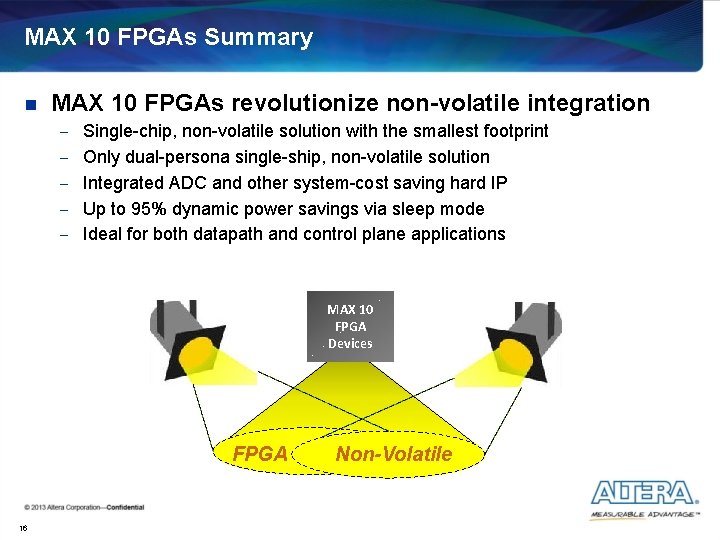
MAX 10 FPGAs Summary n MAX 10 FPGAs revolutionize non-volatile integration - Single-chip, non-volatile solution with the smallest footprint - Only dual-persona single-ship, non-volatile solution - Integrated ADC and other system-cost saving hard IP - Up to 95% dynamic power savings via sleep mode - Ideal for both datapath and control plane applications MAX 10 FPGA Devices FPGA 16 Non-Volatile
What’s Next? n 1 H 2014 Early Information Program n 2 H 2014 Devices & Dev Kits Shipping Would you sign-up for monthly email updates on MAX 10 FPGAs (with valid NDA)? 17
Confidential Material Back-Up Information
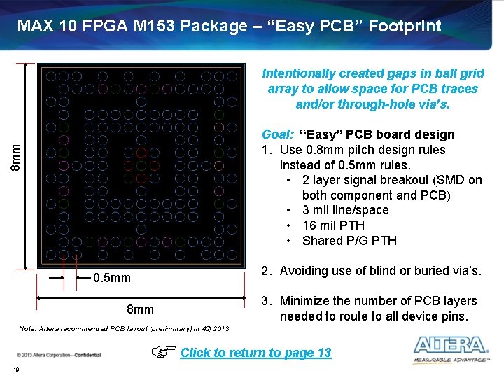
MAX 10 FPGA M 153 Package – “Easy PCB” Footprint Intentionally created gaps in ball grid array to allow space for PCB traces and/or through-hole via’s. 8 mm Goal: “Easy” PCB board design 1. Use 0. 8 mm pitch design rules instead of 0. 5 mm rules. • 2 layer signal breakout (SMD on both component and PCB) • 3 mil line/space • 16 mil PTH • Shared P/G PTH 2. Avoiding use of blind or buried via’s. 0. 5 mm 8 mm 3. Minimize the number of PCB layers needed to route to all device pins. Note: Altera recommended PCB layout (preliminary) in 4 Q 2013 19 Click to return to page 13
Thank You