CONDUCTIVITY q Conductivity q Superconductivity Mechanisms of conduction
![The flux due to flow of electrons → Current density (Je) [charge/area/time] § n The flux due to flow of electrons → Current density (Je) [charge/area/time] § n](https://slidetodoc.com/presentation_image_h2/42554ebae21fcf5877b973e8b023c0db/image-18.jpg)
![Cu, Cu-Ni alloy Resistivity ( ) [x 10 -8 Ohm m] → Increased phonon Cu, Cu-Ni alloy Resistivity ( ) [x 10 -8 Ohm m] → Increased phonon](https://slidetodoc.com/presentation_image_h2/42554ebae21fcf5877b973e8b023c0db/image-21.jpg)


- Slides: 40

CONDUCTIVITY q Conductivity q Superconductivity

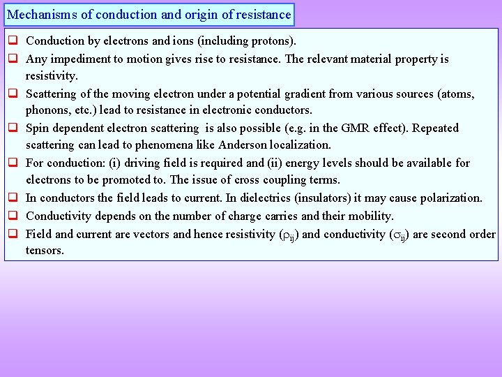
Mechanisms of conduction and origin of resistance q Conduction by electrons and ions (including protons). q Any impediment to motion gives rise to resistance. The relevant material property is resistivity. q Scattering of the moving electron under a potential gradient from various sources (atoms, phonons, etc. ) lead to resistance in electronic conductors. q Spin dependent electron scattering is also possible (e. g. in the GMR effect). Repeated scattering can lead to phenomena like Anderson localization. q For conduction: (i) driving field is required and (ii) energy levels should be available for electrons to be promoted to. The issue of cross coupling terms. q In conductors the field leads to current. In dielectrics (insulators) it may cause polarization. q Conductivity depends on the number of charge carries and their mobility. q Field and current are vectors and hence resistivity ( ij) and conductivity ( ij) are second order tensors.

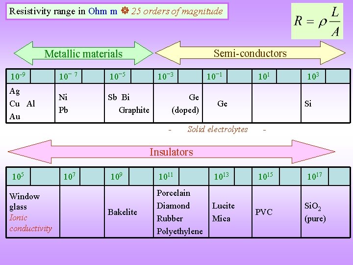
Resistivity range in Ohm m 25 orders of magnitude Semi-conductors Metallic materials 10 9 10 7 10 5 Ag Cu Al Au Ni Pb Sb Bi Graphite 10 3 10 1 Ge (doped) - 101 Ge Solid electrolytes 103 Si - Insulators 105 Window glass Ionic conductivity 107 109 Bakelite 1011 1013 1015 1017 Porcelain Diamond Rubber Polyethylene Lucite Mica PVC Si. O 2 (pure)

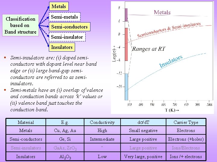
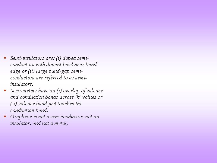
Metals Classification based on Band structure Semi-metals Semi-conductors Semi-insulator Insulators § Semi-insulators are: (i) doped semiconductors with dopant level near band edge or (ii) large band-gap semiconductors are referred to as semiinsulators. § Semi-metals have an (i) overlap of valence and conduction bands across ‘k’ values or (ii) valence band just touches the conduction band. Material E. g. Conductivity d /d. T Carrier Type Metals Cu, Ag, Au High Small negative Electrons Semi-conductors Ge, Si Intermediate Large positive Electrons (+holes) Semi-insulators Ga. As, Zr. O 2 “ Large positive Ions/Electrons Insulators Al 2 O 3 Low Very large, positive Ions /+ electrons

§ Semi-insulators are: (i) doped semiconductors with dopant level near band edge or (ii) large band-gap semiconductors are referred to as semiinsulators. § Semi-metals have an (i) overlap of valence and conduction bands across ‘k’ values or (ii) valence band just touches the conduction band. § Graphene is not a semiconductor, not an insulator, and not a metal,

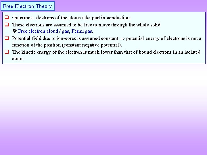
Free Electron Theory q Outermost electrons of the atoms take part in conduction. q These electrons are assumed to be free to move through the whole solid Free electron cloud / gas, Fermi gas. q Potential field due to ion-cores is assumed constant potential energy of electrons is not a function of the position (constant negative potential). q The kinetic energy of the electron is much lower than that of bound electrons in an isolated atom.

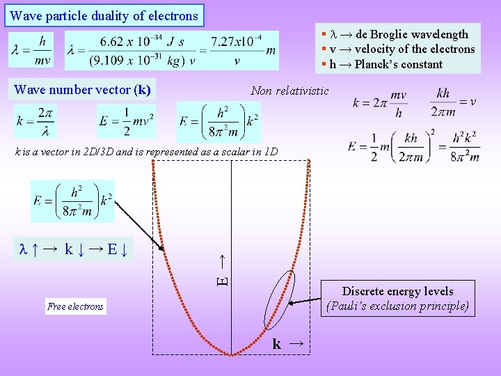
Wave particle duality of electrons § → de Broglie wavelength § v → velocity of the electrons § h → Planck’s constant Wave number vector (k) Non relativistic ↑→ k↓→E↓ E → k is a vector in 2 D/3 D and is represented as a scalar in 1 D Discrete energy levels (Pauli’s exclusion principle) Free electrons k →

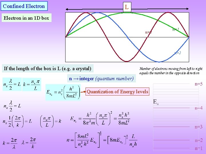
Confined Electron L Electron in an 1 D box n=3 n=1 n=2 If the length of the box is L (e. g. a crystal) Number of electrons moving from left to right equals the number in the opposite direction n → integer (quantum number) Quantization of Energy levels

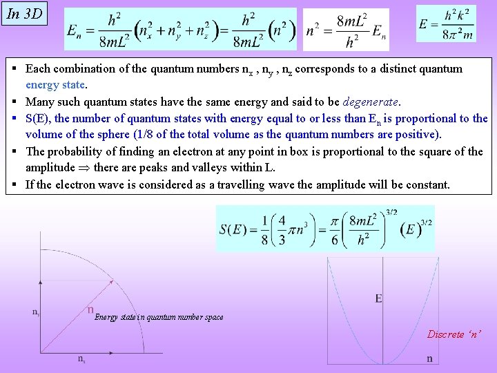
In 3 D § Each combination of the quantum numbers nx , ny , nz corresponds to a distinct quantum energy state. § Many such quantum states have the same energy and said to be degenerate. § S(E), the number of quantum states with energy equal to or less than En is proportional to the volume of the sphere (1/8 of the total volume as the quantum numbers are positive). § The probability of finding an electron at any point in box is proportional to the square of the amplitude there are peaks and valleys within L. § If the electron wave is considered as a travelling wave the amplitude will be constant. Energy state in quantum number space Discrete ‘n’

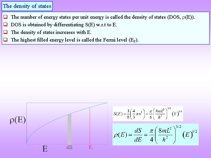
The density of states q q The number of energy states per unit energy is called the density of states (DOS, (E)). DOS is obtained by differentiating S(E) w. r. t to E. The density of states increases with E. The highest filled energy level is called the Fermi level (EF).

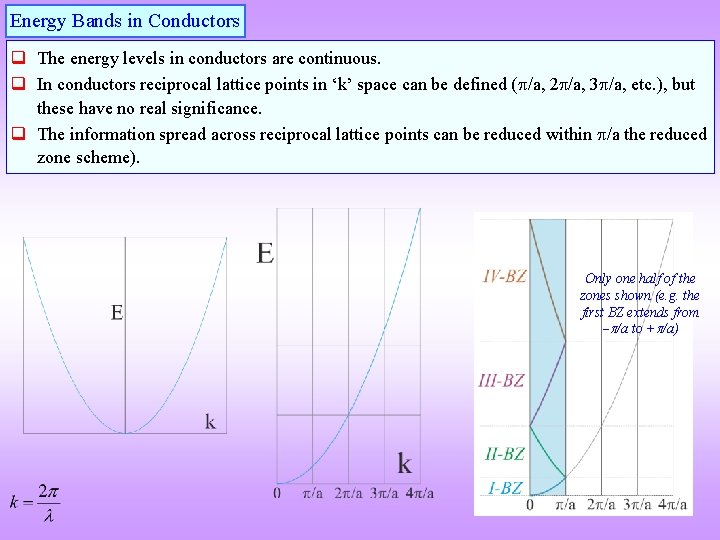
Energy Bands in Conductors q The energy levels in conductors are continuous. q In conductors reciprocal lattice points in ‘k’ space can be defined ( /a, 2 /a, 3 /a, etc. ), but these have no real significance. q The information spread across reciprocal lattice points can be reduced within /a the reduced zone scheme). Only one half of the zones shown (e. g. the first BZ extends from /a to + /a)

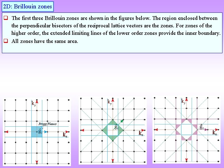
2 D: Brillouin zones q The first three Brillouin zones are shown in the figures below. The region enclosed between the perpendicular bisectors of the reciprocal lattice vectors are the zones. For zones of the higher order, the extended limiting lines of the lower order zones provide the inner boundary. q All zones have the same area.

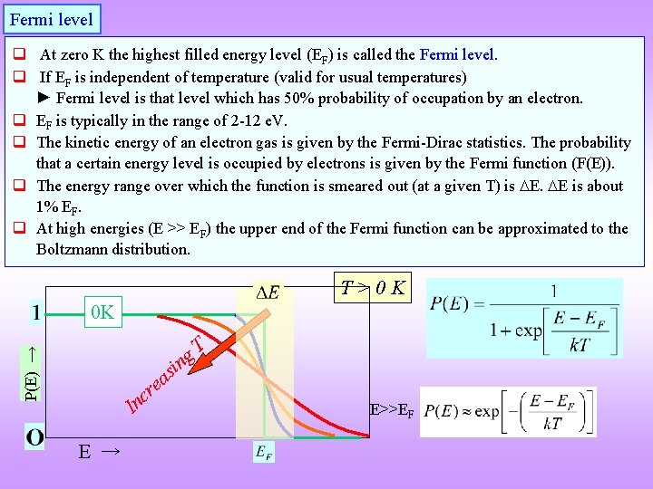
Fermi level q At zero K the highest filled energy level (EF) is called the Fermi level. q If EF is independent of temperature (valid for usual temperatures) ► Fermi level is that level which has 50% probability of occupation by an electron. q EF is typically in the range of 2 -12 e. V. q The kinetic energy of an electron gas is given by the Fermi-Dirac statistics. The probability that a certain energy level is occupied by electrons is given by the Fermi function (F(E)). q The energy range over which the function is smeared out (at a given T) is E. E is about 1% EF. q At high energies (E >> EF) the upper end of the Fermi function can be approximated to the Boltzmann distribution. T>0 K P(E) → 0 K i ng s a e r c n I E → T E>>EF

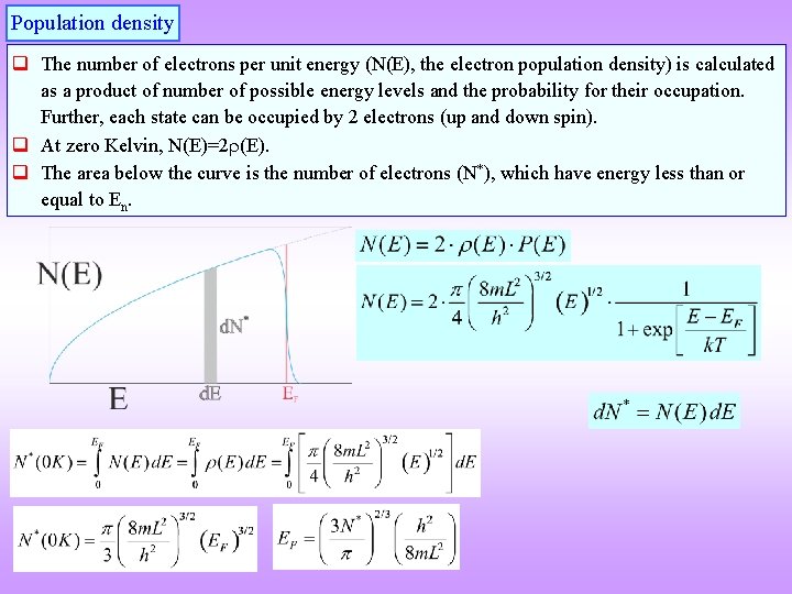
Population density q The number of electrons per unit energy (N(E), the electron population density) is calculated as a product of number of possible energy levels and the probability for their occupation. Further, each state can be occupied by 2 electrons (up and down spin). q At zero Kelvin, N(E)=2 (E). q The area below the curve is the number of electrons (N*), which have energy less than or equal to En.

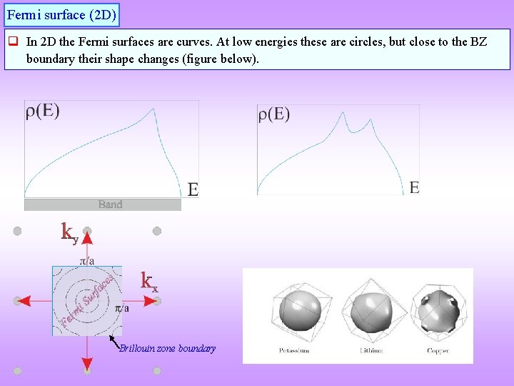
Fermi surface (2 D) q In 2 D the Fermi surfaces are curves. At low energies these are circles, but close to the BZ boundary their shape changes (figure below). Brillouin zone boundary

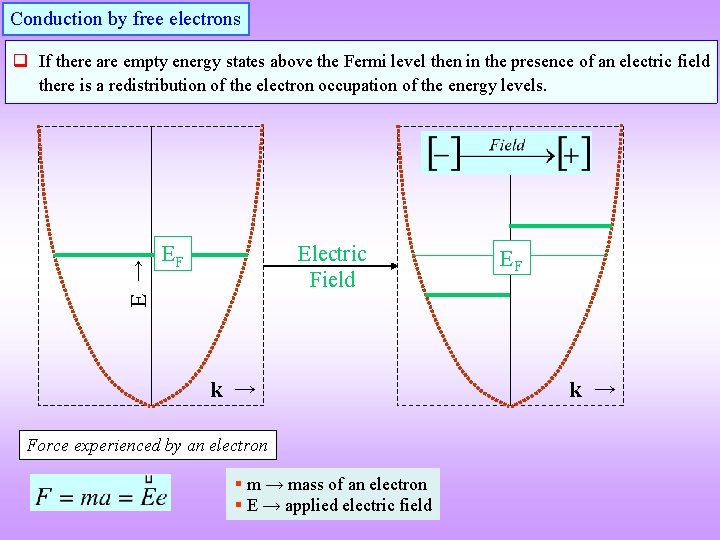
Conduction by free electrons E → q If there are empty energy states above the Fermi level then in the presence of an electric field there is a redistribution of the electron occupation of the energy levels. Electric Field EF k → Force experienced by an electron § m → mass of an electron § E → applied electric field EF k →

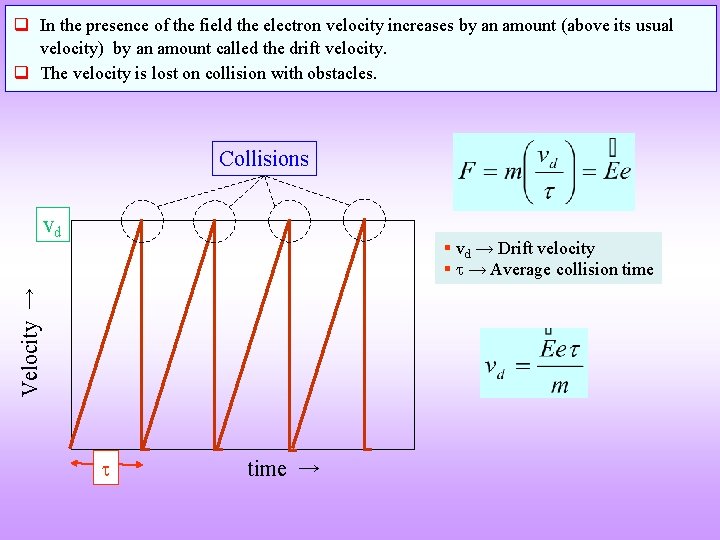
q In the presence of the field the electron velocity increases by an amount (above its usual velocity) by an amount called the drift velocity. q The velocity is lost on collision with obstacles. Collisions vd Velocity → § vd → Drift velocity § → Average collision time →
![The flux due to flow of electrons Current density Je chargeareatime n The flux due to flow of electrons → Current density (Je) [charge/area/time] § n](https://slidetodoc.com/presentation_image_h2/42554ebae21fcf5877b973e8b023c0db/image-18.jpg)
The flux due to flow of electrons → Current density (Je) [charge/area/time] § n → number of free electrons ~ Ohm’s law Actually n has to be replaced by n* and m by m*. n* is the number of electrons at the Fermi level

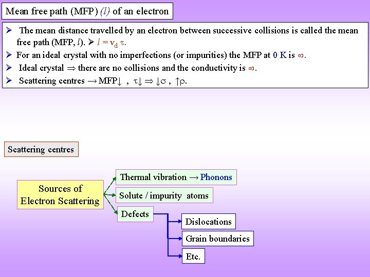
Mean free path (MFP) (l) of an electron The mean distance travelled by an electron between successive collisions is called the mean free path (MFP, l). l = vd . For an ideal crystal with no imperfections (or impurities) the MFP at 0 K is . Ideal crystal there are no collisions and the conductivity is . Scattering centres → MFP↓ , ↓ ↓ , ↑. Scattering centres Thermal vibration → Phonons Sources of Electron Scattering Solute / impurity atoms Defects Dislocations Grain boundaries Etc.

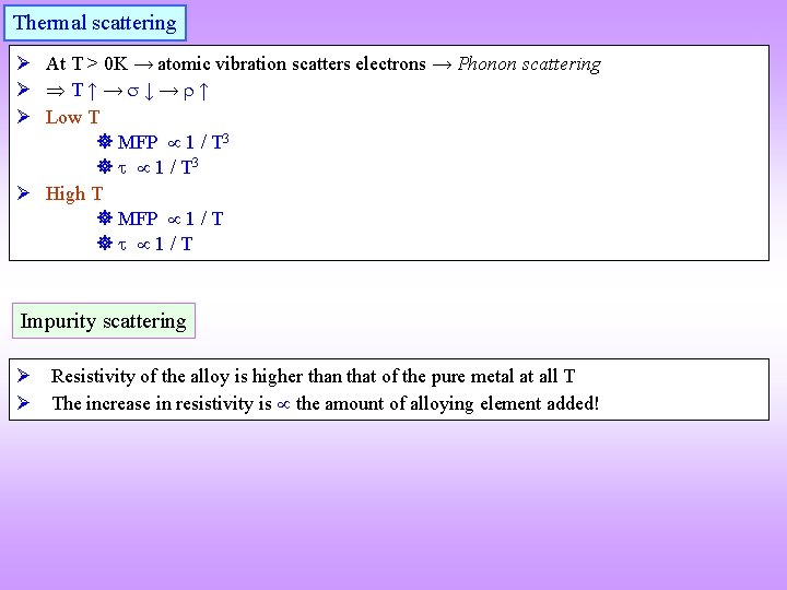
Thermal scattering At T > 0 K → atomic vibration scatters electrons → Phonon scattering T↑→ ↓→ ↑ Low T MFP 1 / T 3 High T MFP 1 / T Impurity scattering Resistivity of the alloy is higher than that of the pure metal at all T The increase in resistivity is the amount of alloying element added!
![Cu CuNi alloy Resistivity x 10 8 Ohm m Increased phonon Cu, Cu-Ni alloy Resistivity ( ) [x 10 -8 Ohm m] → Increased phonon](https://slidetodoc.com/presentation_image_h2/42554ebae21fcf5877b973e8b023c0db/image-21.jpg)
Cu, Cu-Ni alloy Resistivity ( ) [x 10 -8 Ohm m] → Increased phonon scattering 5 Cu-3%Ni 4 Cu-2%Ni 3 2 1 Impurity scattering ( r) With low density of imperfections Pure Cu → 0 as T→ 0 K 100 200 300 T (K) → Mattheissen rule = T + r Net resistivity (approx. ) = Thermal resistivity + Resistivity due to impurity scattering

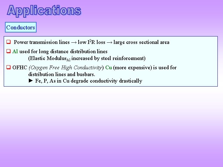
Conductors q Power transmission lines → low I 2 R loss → large cross sectional area q Al used for long distance distribution lines (Elastic Modulus. Al increased by steel reinforcement) q OFHC (Oxygen Free High Conductivity) Cu (more expensive) is used for distribution lines and busbars. ► Fe, P, As in Cu degrade conductivity drastically

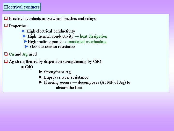
Electrical contacts q Electrical contacts in switches, brushes and relays q Properties: ► High electrical conductivity ► High thermal conductivity → heat dissipation ►High melting point → accidental overheating ► Good oxidation resistance q Cu and Ag used q Ag strengthened by dispersion strengthening by Cd. O ■ Cd. O ► Strengthens Ag ► Improves wear resistance ► If arcing occurs → decomposes (At MP of Ag) to absorb the heat

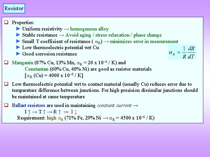
Resistor q Properties: ► Uniform resistivity → homogenous alloy ► Stable resistance → Avoid aging / stress relaxation / phase change ► Small T coefficient of resistance ( R) → minimizes error in measurement ► Low thermoelectric potential wrt Cu ► Good corrosion resistance q Manganin (87% Cu, 13% Mn, R = 20 x 10 6 / K) and Constantan (60% Cu, 40% Ni) are good as resistor materials [ R (Cu) = 4000 x 10 6 / K] q Low thermoelectric potential wrt to contact material (usually Cu) reduces error due to temperature difference between junctions. For high precision dissimilar junctions should be maintained at same temperature q Ballast resistors are used in maintaining constant current → I↑→T↑→R↑ I↓ Requirement: high R (71% Fe, 29% Ni → R = 4500 x 10 6 / K)

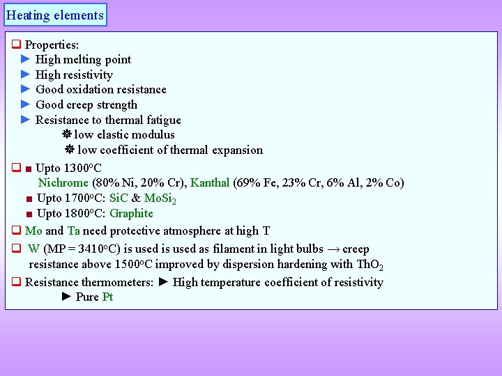
Heating elements q Properties: ► High melting point ► High resistivity ► Good oxidation resistance ► Good creep strength ► Resistance to thermal fatigue low elastic modulus low coefficient of thermal expansion q ■ Upto 1300 o. C Nichrome (80% Ni, 20% Cr), Kanthal (69% Fe, 23% Cr, 6% Al, 2% Co) ■ Upto 1700 o. C: Si. C & Mo. Si 2 ■ Upto 1800 o. C: Graphite q Mo and Ta need protective atmosphere at high T q W (MP = 3410 o. C) is used as filament in light bulbs → creep resistance above 1500 o. C improved by dispersion hardening with Th. O 2 q Resistance thermometers: ► High temperature coefficient of resistivity ► Pure Pt

SUPERCONDUCTIVITY

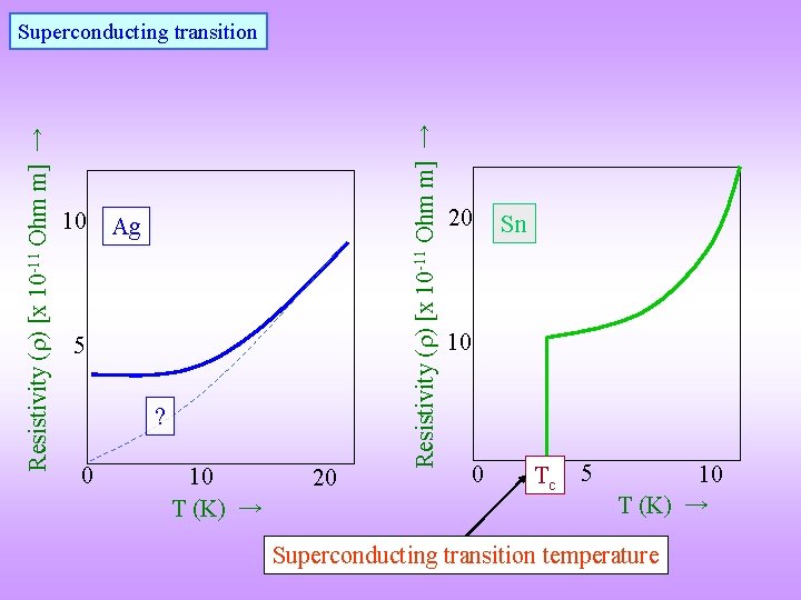
10 Ag 5 ? 0 10 T (K) → 20 Resistivity ( ) [x 10 -11 Ohm m] → Superconducting transition 20 Sn 10 0 Tc 5 10 T (K) → Superconducting transition temperature

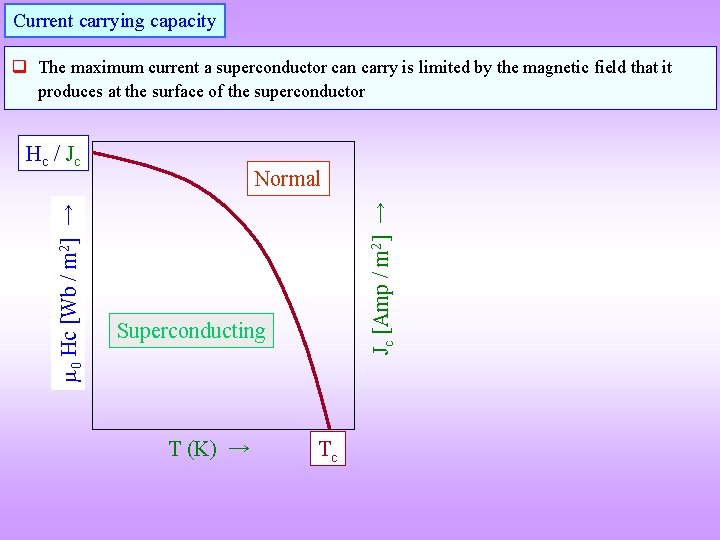
Current carrying capacity q The maximum current a superconductor can carry is limited by the magnetic field that it produces at the surface of the superconductor Normal Jc [Amp / m 2] → 0 Hc [Wb / m 2] → Hc / Jc Superconducting T (K) → Tc

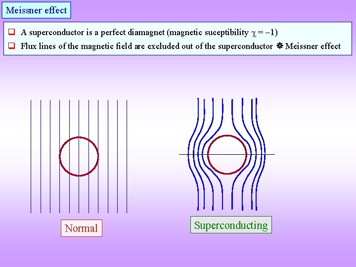
Meissner effect q A superconductor is a perfect diamagnet (magnetic suceptibility = 1) q Flux lines of the magnetic field are excluded out of the superconductor Meissner effect Normal Superconducting

Theory of low temperature superconductivity. Bardeen-Cooper-Schreiffer (BCS) theory q Three way interaction between an two electron and a phonon q Phonon scattering due to lattice vibrations felt by one electron in the Cooper pair is nullified by the other electron in the pair the electron pair moves through the lattice without getting scattered by the lattice vibrations q The force of attraction between the electrons in the Cooper pair is stronger than the repulsive force between the electrons when T < Tc

Type I and Type II superconductors

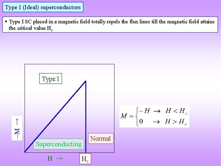
Type I (Ideal) superconductors § Type I SC placed in a magnetic field totally repels the flux lines till the magnetic field attains the critical value Hc M → Type I Normal Superconducting H → Hc

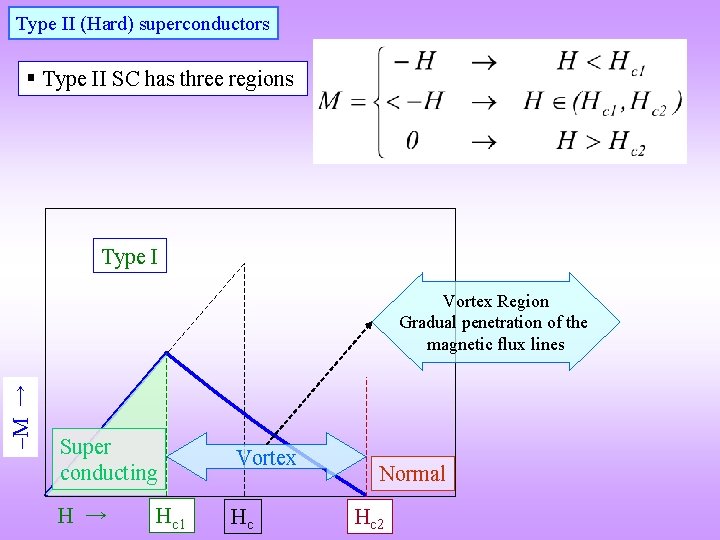
Type II (Hard) superconductors § Type II SC has three regions Type I M → Vortex Region Gradual penetration of the magnetic flux lines Super conducting Vortex H → Hc Hc 1 Normal Hc 2

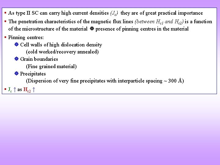
§ As type II SC can carry high current densities (Jc) they are of great practical importance § The penetration characteristics of the magnetic flux lines (between Hc 1 and Hc 2) is a function of the microstructure of the material presence of pinning centres in the material § Pinning centres: Cell walls of high dislocation density (cold worked/recovery annealed) Grain boundaries (Fine grained material) Precipitates (Dispersion of very fine precipitates with interparticle spacing ~ 300 Å) § Jc ↑ as Hc 2 ↑

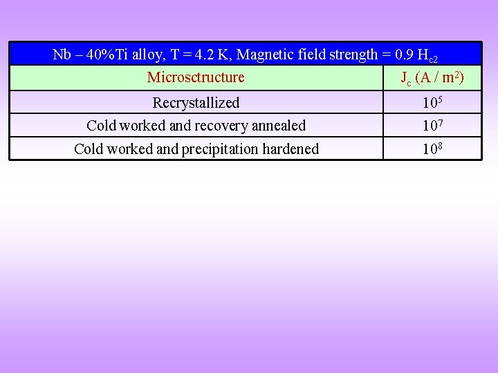
Nb – 40%Ti alloy, T = 4. 2 K, Magnetic field strength = 0. 9 Hc 2 Microsctructure Jc (A / m 2) Recrystallized 105 Cold worked and recovery annealed 107 Cold worked and precipitation hardened 108

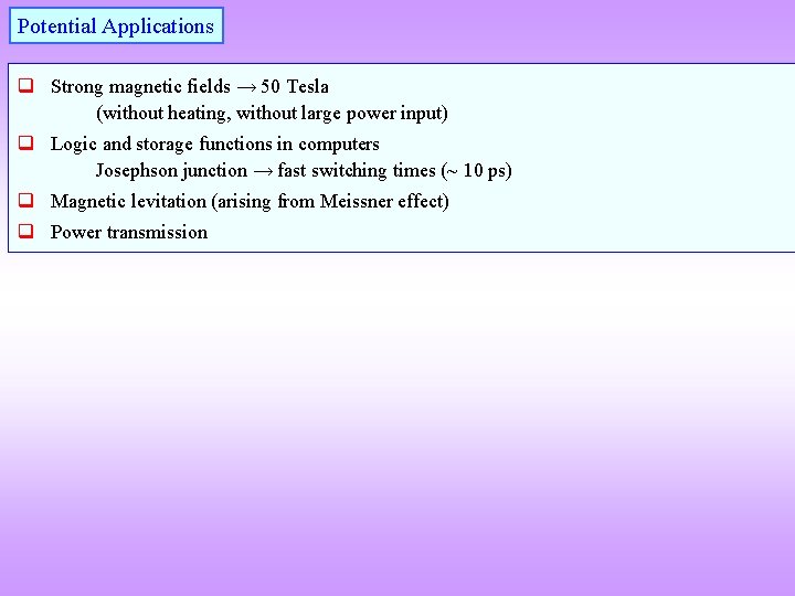
Potential Applications q Strong magnetic fields → 50 Tesla (without heating, without large power input) q Logic and storage functions in computers Josephson junction → fast switching times (~ 10 ps) q Magnetic levitation (arising from Meissner effect) q Power transmission

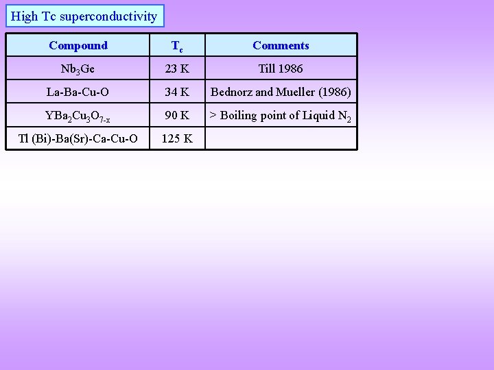
High Tc superconductivity Compound Tc Comments Nb 3 Ge 23 K Till 1986 La-Ba-Cu-O 34 K Bednorz and Mueller (1986) YBa 2 Cu 3 O 7 -x 90 K > Boiling point of Liquid N 2 Tl (Bi)-Ba(Sr)-Ca-Cu-O 125 K

Manufacture of YBa 2 Cu 3 O 7 -x Please read from text book

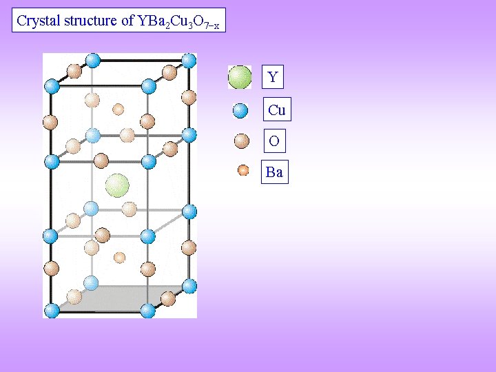
Crystal structure of YBa 2 Cu 3 O 7 x Y Cu O Ba

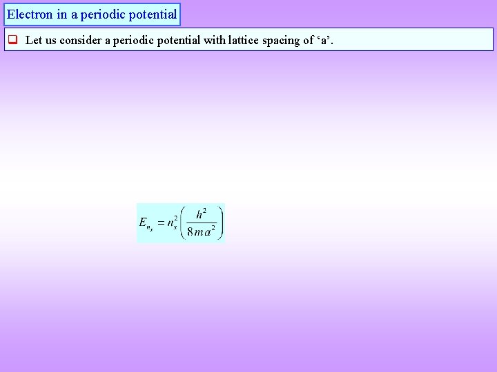
Electron in a periodic potential q Let us consider a periodic potential with lattice spacing of ‘a’.