Conclusion Silicon Diode Si Germanium Diode Ge Atomic

- Slides: 24

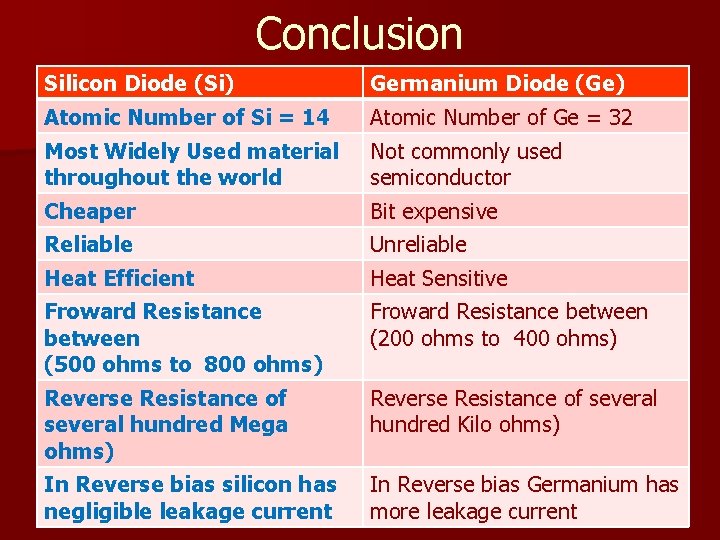
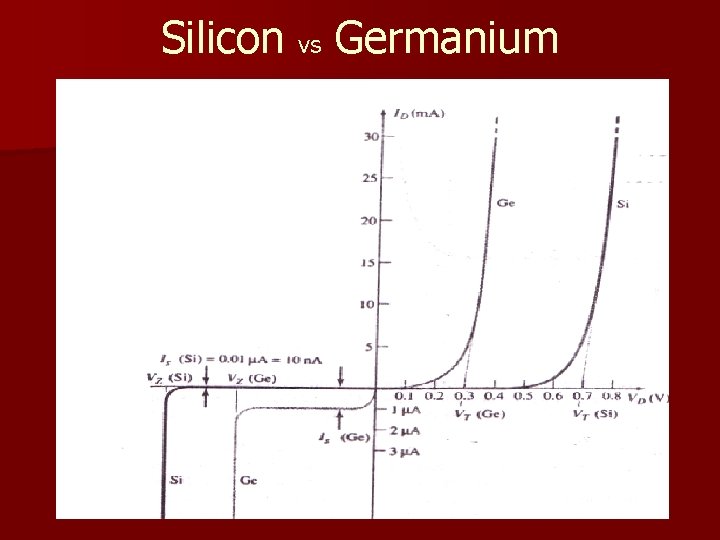
Conclusion Silicon Diode (Si) Germanium Diode (Ge) Atomic Number of Si = 14 Atomic Number of Ge = 32 Most Widely Used material throughout the world Not commonly used semiconductor Cheaper Bit expensive Reliable Unreliable Heat Efficient Heat Sensitive Froward Resistance between (500 ohms to 800 ohms) Froward Resistance between (200 ohms to 400 ohms) Reverse Resistance of several hundred Mega ohms) Reverse Resistance of several hundred Kilo ohms) In Reverse bias silicon has negligible leakage current In Reverse bias Germanium has more leakage current

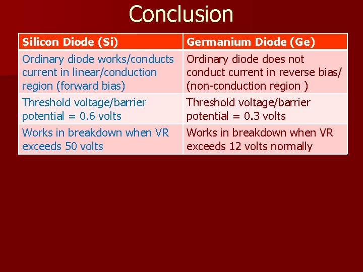
Conclusion Silicon Diode (Si) Germanium Diode (Ge) Ordinary diode works/conducts current in linear/conduction region (forward bias) Ordinary diode does not conduct current in reverse bias/ (non-conduction region ) Threshold voltage/barrier potential = 0. 6 volts Threshold voltage/barrier potential = 0. 3 volts Works in breakdown when VR exceeds 50 volts Works in breakdown when VR exceeds 12 volts normally

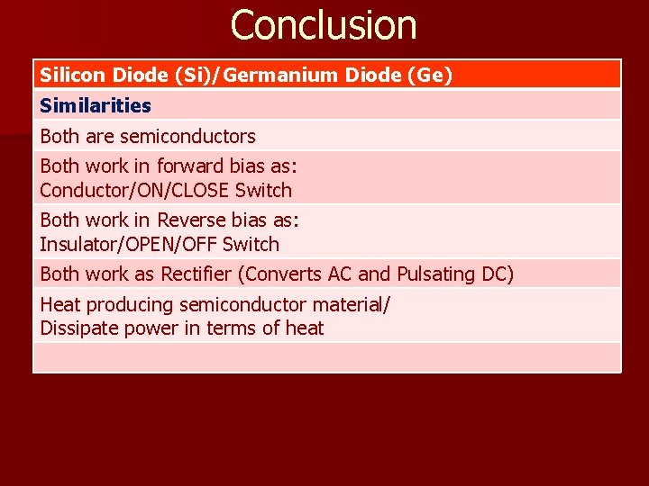
Conclusion Silicon Diode (Si)/Germanium Diode (Ge) Similarities Both are semiconductors Both work in forward bias as: Conductor/ON/CLOSE Switch Both work in Reverse bias as: Insulator/OPEN/OFF Switch Both work as Rectifier (Converts AC and Pulsating DC) Heat producing semiconductor material/ Dissipate power in terms of heat

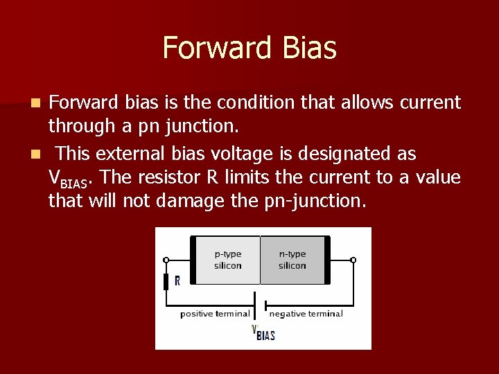
Forward Bias Forward bias is the condition that allows current through a pn junction. n This external bias voltage is designated as VBIAS. The resistor R limits the current to a value that will not damage the pn-junction. n

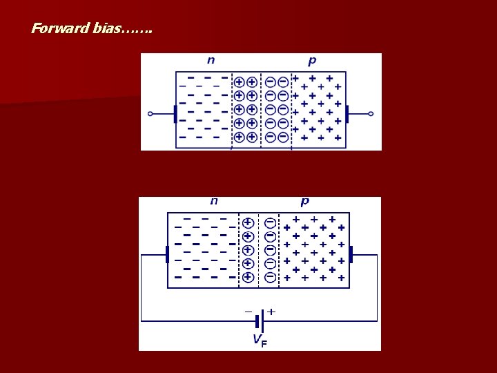
The Effect of Forward Bias on the Depletion Region n As more electrons flow into the depletion region, the number of positive ions is reduced. As more holes effectively flow into the depletion region on the other side of the pn junction, the number of negative ions is reduced. This reduction in positive and negative ions during forward bias causes the depletion region to narrow.

Forward bias…….

Effect of the Barrier Potential During Forward Bias When forward bias is applied, the free electrons are provided with enough energy to overcome the barrier potential and effectively “climb" the energy hill and cross the depletion region. The energy that the electrons require in order to pass through the depletion region is equal to the barrier potential energy. In other words, the electrons give up an amount of energy equivalent to the barrier potential when they cross the depletion region. This energy loss results in a voltage drop across the pn junction

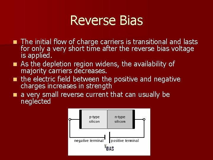
Reverse Bias n n The initial flow of charge carriers is transitional and lasts for only a very short time after the reverse bias voltage is applied. As the depletion region widens, the availability of majority carriers decreases. the electric field between the positive and negative charges increases in strength a very small reverse current that can usually be neglected

Reverse Bias……. . n the width of the depletion zone will increase. This increases the voltage barrier causing a high resistance to the flow of charge carriers thus allowing minimal electric current to cross the p-n junction. n The strength of the depletion zone electric field increases as the reverse-bias voltage increases. Once the electric field intensity increases beyond a critical level, the p-n junction depletion zone breaks-down and current begins to flow, usually by either the Zener or avalanche breakdown processes. .

Reverse Current The small number of free minority electrons in the p region are "pushed" toward the pn junction by the negative bias voltage. When these electrons reach the wide depletion region, they "fall down the energy hill" and combine with the minority holes in the n region as valence electrons and flow toward the positive bias voltage, creating a small hole current. n The minority electrons easily pass through the depletion region because they require no additional energy n

Reverse Breakdown At the breakdown voltage, the reverse current will drastically increase. n The high reverse-bias voltage imparts energy to the free minority electrons so that as they speed through the p region, they collide with atoms with enough energy to knock valence electrons out of orbit. The newly created conduction electrons are also high in energy and repeat the process. If one electron knocks only two others out of their valence orbit during its travel through the h region, the numbers quickly multiply. As these highenergy electrons go through the depletion region, they have enough energy to go through the n region as conduction electrons. rather than combining with holes. n The multiplication of conduction electrons just discussed is known as avalanche and results in a very high reverse current that can damage the pn structure because of excessive heat dissipation. n

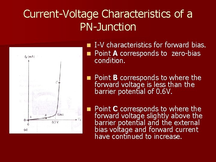
Current-Voltage Characteristics of a PN-Junction n n I-V characteristics forward bias. Point A corresponds to zero-bias condition. n Point B corresponds to where the forward voltage is less than the barrier potential of 0. 6 V. n Point C corresponds to where the forward voltage slightly above the barrier potential and the external bias voltage and forward current have continued to increase.

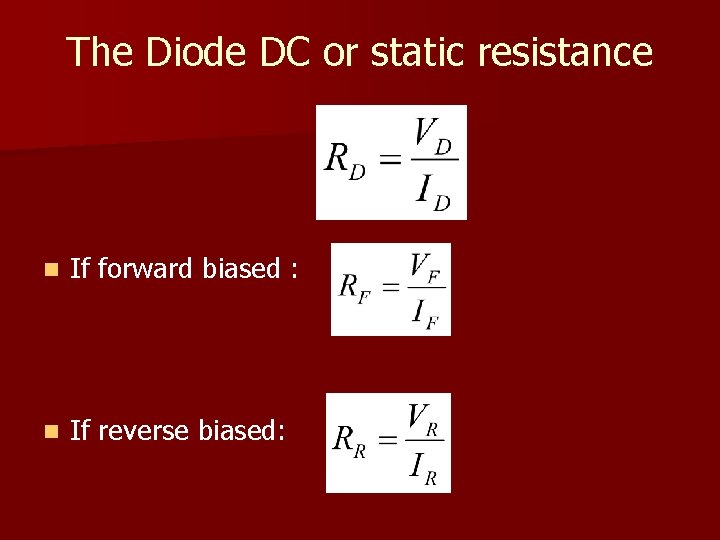
The Diode DC or static resistance n If forward biased : n If reverse biased:

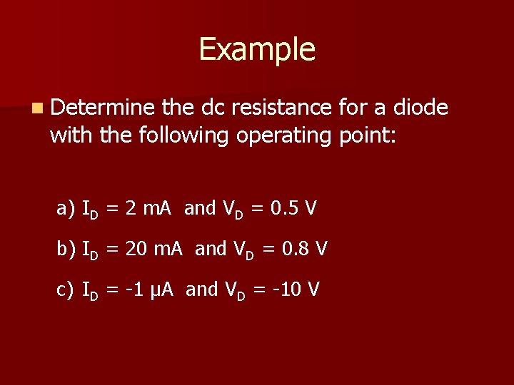
Example n Determine the dc resistance for a diode with the following operating point: a) ID = 2 m. A and VD = 0. 5 V b) ID = 20 m. A and VD = 0. 8 V c) ID = -1 μA and VD = -10 V

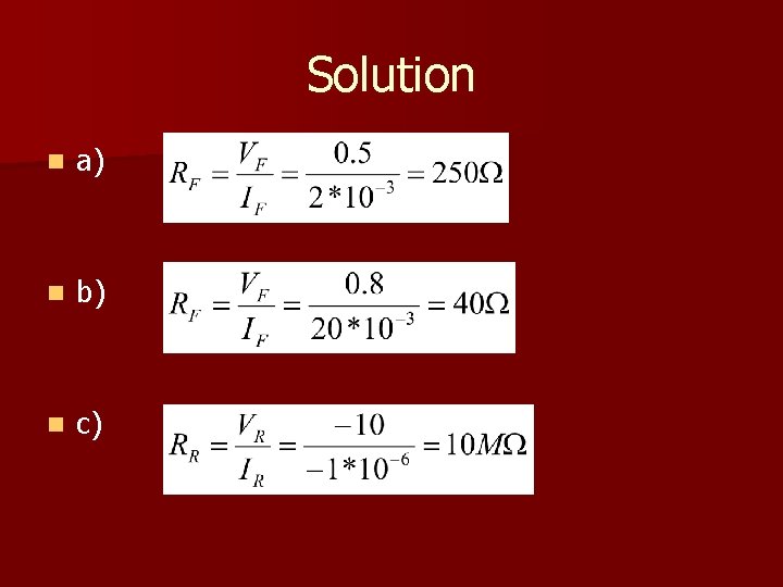
Solution n a) n b) n c)

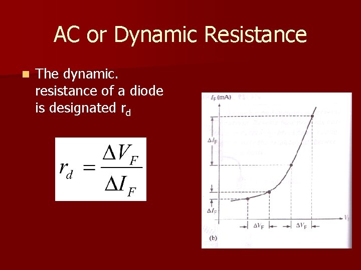
AC or Dynamic Resistance n The dynamic. resistance of a diode is designated rd

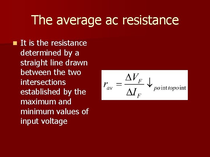
The average ac resistance n It is the resistance determined by a straight line drawn between the two intersections established by the maximum and minimum values of input voltage

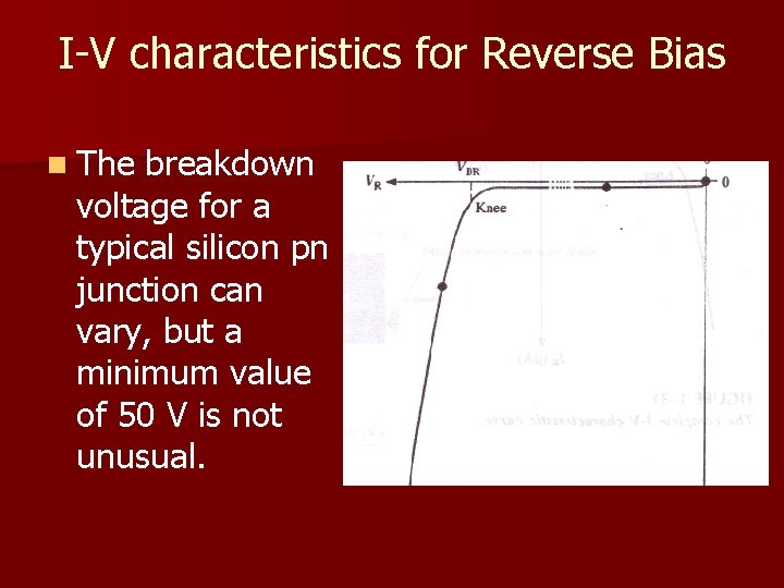
I-V characteristics for Reverse Bias n The breakdown voltage for a typical silicon pn junction can vary, but a minimum value of 50 V is not unusual.

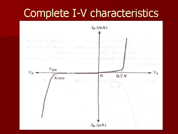
Complete I-V characteristics

Silicon vs Germanium

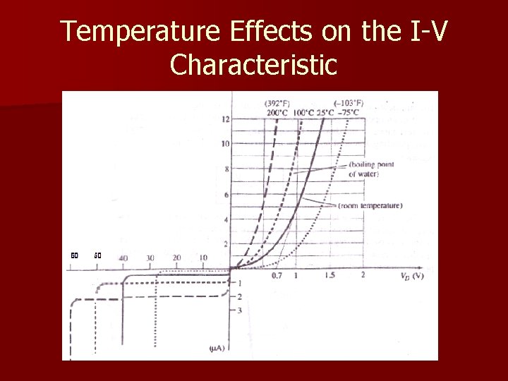
Temperature Effects on the I-V Characteristic

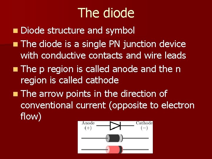
The diode n Diode structure and symbol n The diode is a single PN junction device with conductive contacts and wire leads n The p region is called anode and the n region is called cathode n The arrow points in the direction of conventional current (opposite to electron flow)

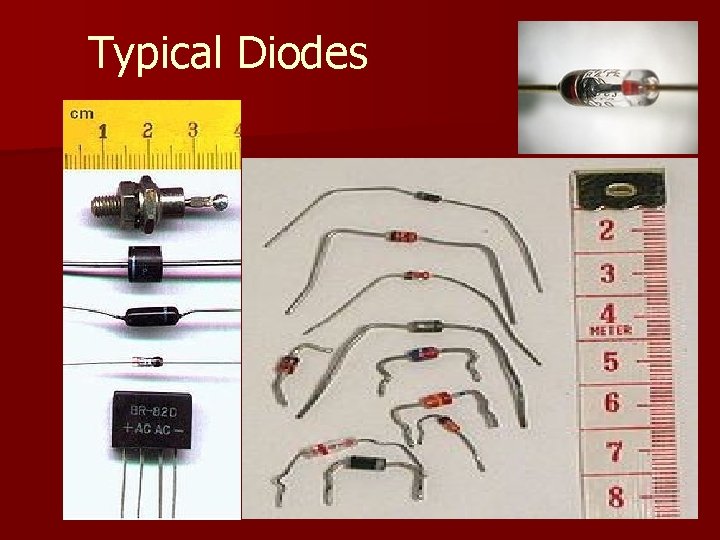
Typical Diodes

n Discussion n Question/Answer