ComputerAided Design of Digital VLSI Circuits Systems Perspectives
- Slides: 23

Computer-Aided Design of Digital VLSI Circuits & Systems Perspectives on Next-Generation Logic Synthesis Priyank Kalla Dept. of Elec. & Comp. Engineering University of Utah, SLC

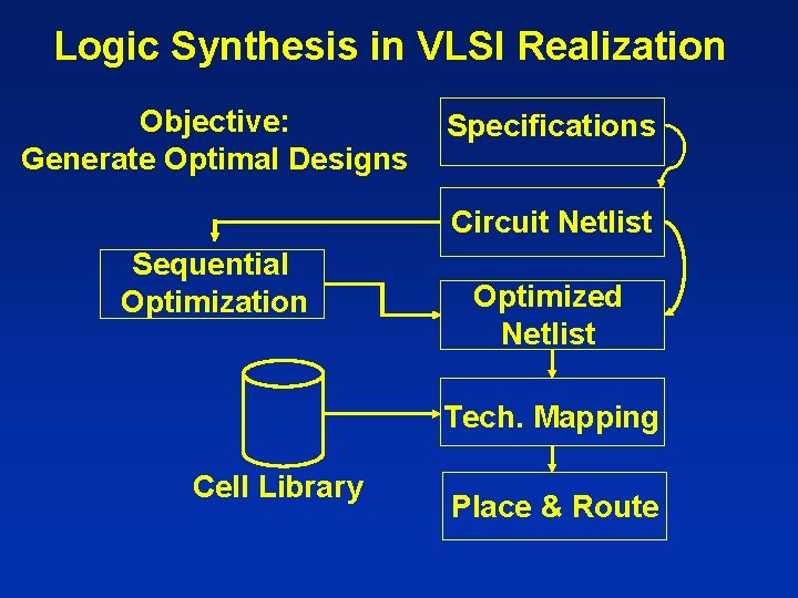
Logic Synthesis in VLSI Realization Objective: Generate Optimal Designs Specifications Circuit Netlist Sequential Optimization Optimized Netlist Tech. Mapping Cell Library Place & Route

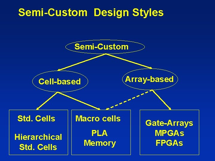
Semi-Custom Design Styles Semi-Custom Array-based Cell-based Std. Cells Macro cells Hierarchical Std. Cells PLA Memory Gate-Arrays MPGAs FPGAs

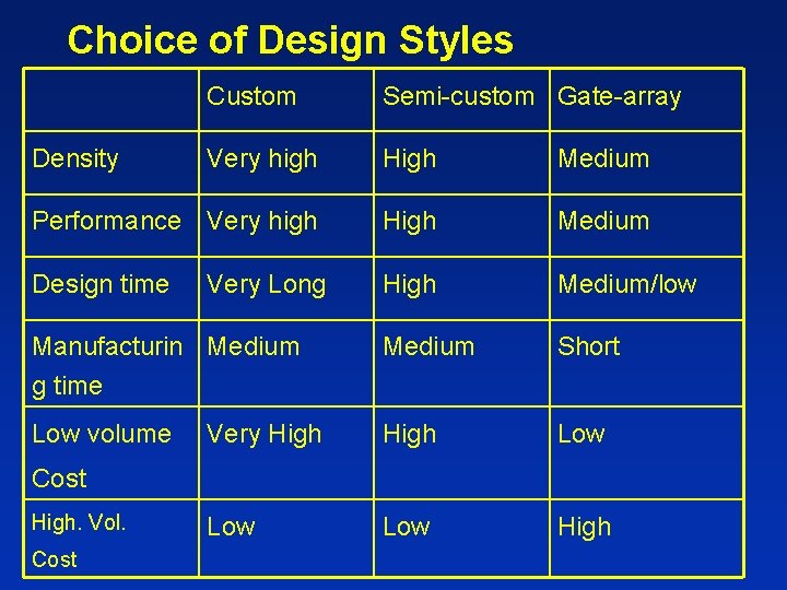
Choice of Design Styles Custom Semi-custom Gate-array Very high High Medium Performance Very high High Medium Design time High Medium/low Manufacturin Medium g time Medium Short Low volume Very High Low Low High Density Very Long Cost High. Vol. Cost

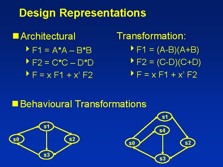
Design Representations g Architectural 4 F 1 = A*A – B*B 4 F 2 = C*C – D*D 4 F = x F 1 + x’ F 2 g Behavioural Transformation: 4 F 1 = (A-B)(A+B) 4 F 2 = (C-D)(C+D) 4 F = x F 1 + x’ F 2 Transformations s 1 s 4 s 2 s 0 s 3

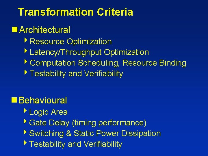
Transformation Criteria g Architectural 4 Resource Optimization 4 Latency/Throughput Optimization 4 Computation Scheduling, Resource Binding 4 Testability and Verifiability g Behavioural 4 Logic Area 4 Gate Delay (timing performance) 4 Switching & Static Power Dissipation 4 Testability and Verifiability

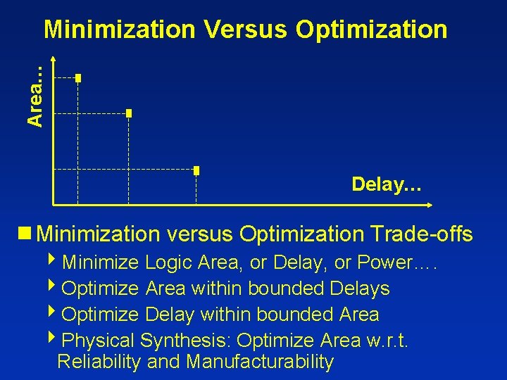
Area… Minimization Versus Optimization Delay… g Minimization versus Optimization Trade-offs 4 Minimize Logic Area, or Delay, or Power…. 4 Optimize Area within bounded Delays 4 Optimize Delay within bounded Area 4 Physical Synthesis: Optimize Area w. r. t. Reliability and Manufacturability

What is Logic Synthesis? g Given: Logic Functions or Finite-State Machines 4 Automatically generate designs (synthesis) 4 Minimize or Optimize Logic w. r. t. constraints 4 Optimally map logic onto realistic gates g Problems and Challenges 4 Memory: Size! SIZE! 4 Time: Computationally intensive operations 4 What kind of representations to use? 4 How to optimize logic to target the technology?

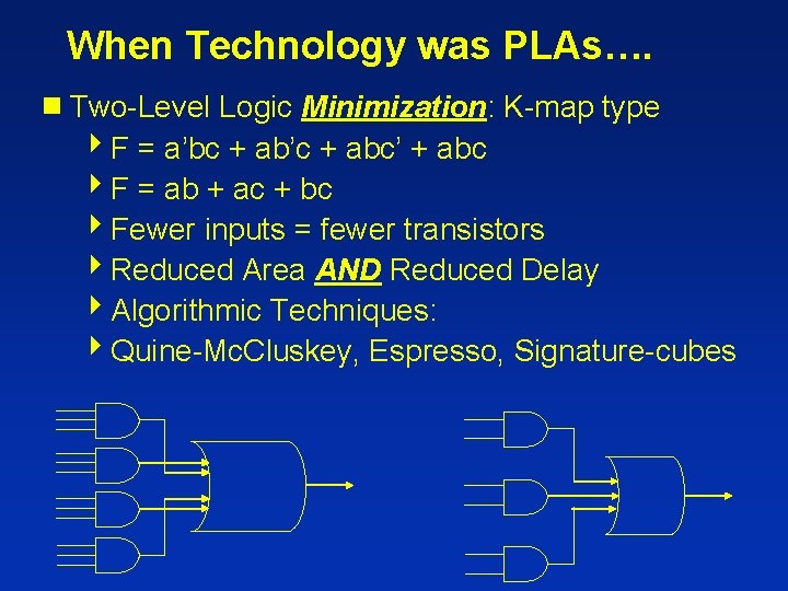
When Technology was PLAs…. g Two-Level Logic Minimization: K-map type 4 F = a’bc + ab’c + abc’ + abc 4 F = ab + ac + bc 4 Fewer inputs = fewer transistors 4 Reduced Area AND Reduced Delay 4 Algorithmic Techniques: 4 Quine-Mc. Cluskey, Espresso, Signature-cubes

Then came CMOS Technology…. g Salient Features: 4 Very high noise margins 4 Design Scalability 4 Enabled Standard Cell-based Design 4 Abstract Electrical Properties: Area-Delay 4 Fanout-Drive Scalability: X’sistor Sizing 4 Low (zero) Static Power Dissipation 4 Enabled Standard-Cell Place & Route 4 Estimates: Close to ~10% of actual layout 4 Cheap, Reliable, Scalable, low turn-aournd time

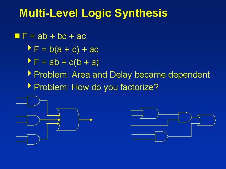
Multi-Level Logic Synthesis g. F = ab + bc + ac 4 F = b(a + c) + ac 4 F = ab + c(b + a) 4 Problem: Area and Delay became dependent 4 Problem: How do you factorize?

Multi-Level Synthesis for CMOS g Synthesis Issues to consider 4 Objective: Minimize number of literals (area) 4 Delay: Depth of paths, fanouts, signal orders, arrival and required times…. 4 Area Delay became dependent 4 Factorization: 4 Extract common subexpressions 4 Fanout problems 4 Routing Difficulties 4 Optimization (instead of minimization) became the dominant issue

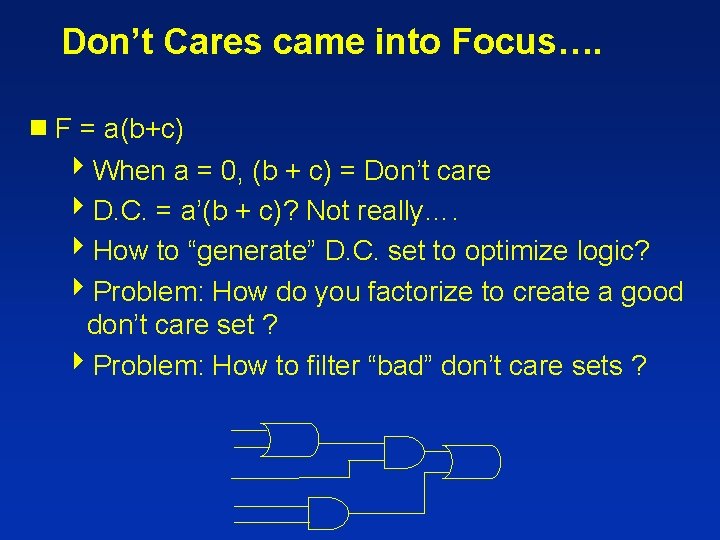
Don’t Cares came into Focus…. g. F = a(b+c) 4 When a = 0, (b + c) = Don’t care 4 D. C. = a’(b + c)? Not really…. 4 How to “generate” D. C. set to optimize logic? 4 Problem: How do you factorize to create a good don’t care set ? 4 Problem: How to filter “bad” don’t care sets ?

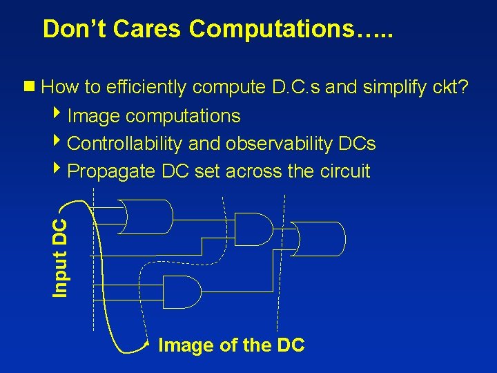
Don’t Cares Computations…. . to efficiently compute D. C. s and simplify ckt? 4 Image computations 4 Controllability and observability DCs 4 Propagate DC set across the circuit Input DC g How Image of the DC

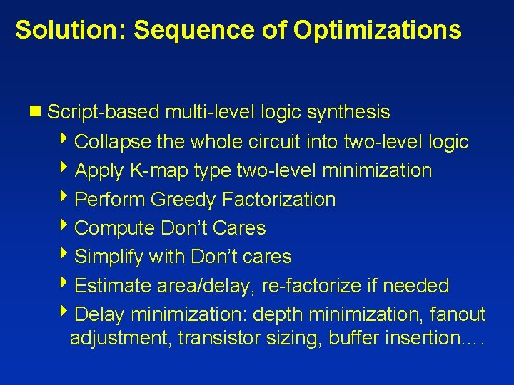
Solution: Sequence of Optimizations g Script-based multi-level logic synthesis 4 Collapse the whole circuit into two-level logic 4 Apply K-map type two-level minimization 4 Perform Greedy Factorization 4 Compute Don’t Cares 4 Simplify with Don’t cares 4 Estimate area/delay, re-factorize if needed 4 Delay minimization: depth minimization, fanout adjustment, transistor sizing, buffer insertion….

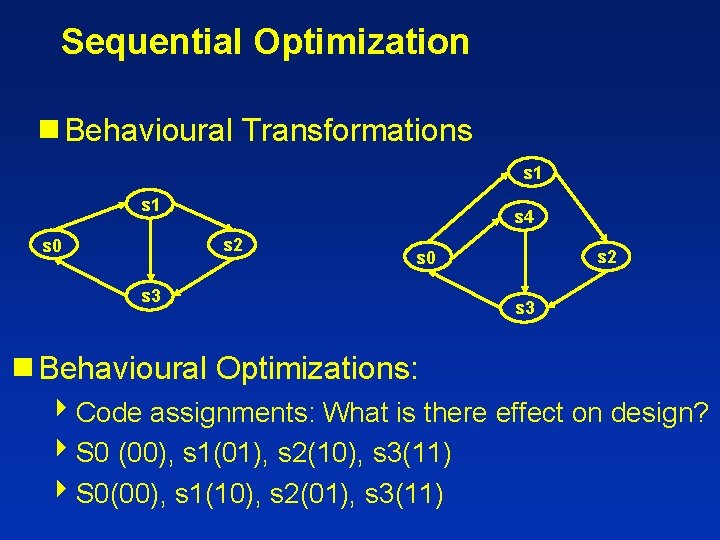
Sequential Optimization g Behavioural Transformations s 1 s 4 s 2 s 0 s 3 g Behavioural s 2 s 0 s 3 Optimizations: 4 Code assignments: What is there effect on design? 4 S 0 (00), s 1(01), s 2(10), s 3(11) 4 S 0(00), s 1(10), s 2(01), s 3(11)

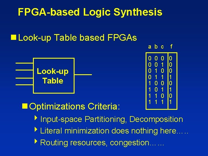
FPGA-based Logic Synthesis g Look-up Table based FPGAs Look-up Table g Optimizations Criteria: a b c f 0 0 1 1 0 0 0 1 0 1 0 0 1 1 0 1 0 1 4 Input-space Partitioning, Decomposition 4 Literal minimization does nothing here…. . 4 Routing resources, congestion……

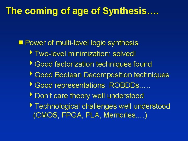
The coming of age of Synthesis…. g Power of multi-level logic synthesis 4 Two-level minimization: solved! 4 Good factorization techniques found 4 Good Boolean Decomposition techniques 4 Good representations: ROBDDs…. . 4 Don’t care theory well understood 4 Technological challenges well understood (CMOS, FPGA, PLA, Memories…. )

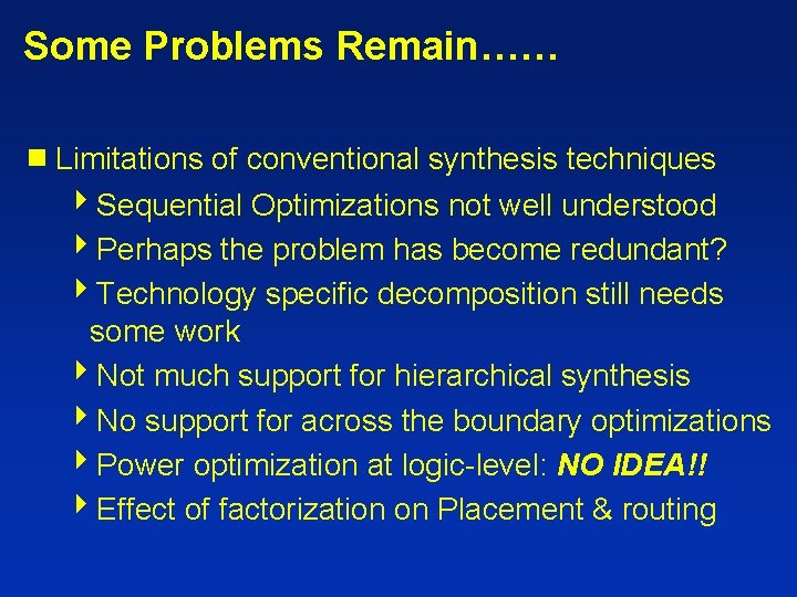
Some Problems Remain…… g Limitations of conventional synthesis techniques 4 Sequential Optimizations not well understood 4 Perhaps the problem has become redundant? 4 Technology specific decomposition still needs some work 4 Not much support for hierarchical synthesis 4 No support for across the boundary optimizations 4 Power optimization at logic-level: NO IDEA!! 4 Effect of factorization on Placement & routing

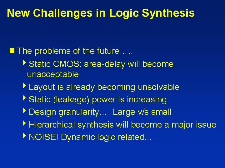
New Challenges in Logic Synthesis g The problems of the future…. . 4 Static CMOS: area-delay will become unacceptable 4 Layout is already becoming unsolvable 4 Static (leakage) power is increasing 4 Design granularity…. Large v/s small 4 Hierarchical synthesis will become a major issue 4 NOISE! Dynamic logic related….

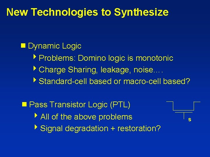
New Technologies to Synthesize g Dynamic Logic 4 Problems: Domino logic is monotonic 4 Charge Sharing, leakage, noise…. 4 Standard-cell based or macro-cell based? g Pass Transistor Logic (PTL) 4 All of the above problems 4 Signal degradation + restoration? s

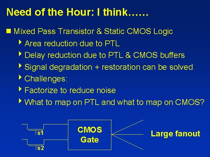
Need of the Hour: I think…… g Mixed Pass Transistor & Static CMOS Logic 4 Area reduction due to PTL 4 Delay reduction due to PTL & CMOS buffers 4 Signal degradation + restoration can be solved 4 Challenges: 4 Factorize to reduce noise 4 What to map on PTL and what to map on CMOS? s 1 s 2 CMOS Gate Large fanout

Need of the Future: I think…… g For new technologies, “nano”-type 4 Area/Delay estimation Rethink 4 Sequential Optimization will bounce back! 4 Binary valued logic to Multi-values Logic 4 Power has to be handled at logic level 4 Memory no problem…. But computation time…. 4 Logic optimization for manufacturability…. . 4 Structured Logic Decomposition for estimatable Placement and routing…. 4 How about “Synthesis for verifiablity” ?