Computer Systems Organization Architecture John D Carpinelli 2001


- Slides: 80


교재 Computer Systems Organization & Architecture John D. Carpinelli, 2001, Addison Wesley


What must you do as a junior student Improve your grade up to at least 3. 5/4. 5. Cultivate your English ability. Make good relationship with your friends. Think your future seriously. Be an expert in your field. Be flexible.

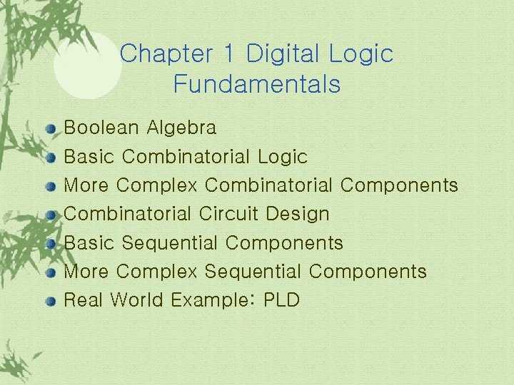
Chapter 1 Digital Logic Fundamentals Boolean Algebra Basic Combinatorial Logic More Complex Combinatorial Components Combinatorial Circuit Design Basic Sequential Components More Complex Sequential Components Real World Example: PLD

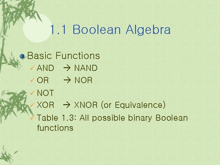
1. 1 Boolean Algebra Basic Functions ü AND ü OR NAND NOR ü NOT XNOR (or Equivalence) ü Table 1. 3: All possible binary Boolean functions ü XOR

1. 1 Boolean Algebra(계속) Manipulation of Boolean Algebra ü De. Morgan’s Law ü Minterm ü Karnaugh map(K-map)

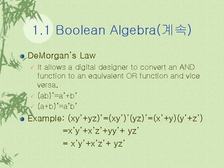
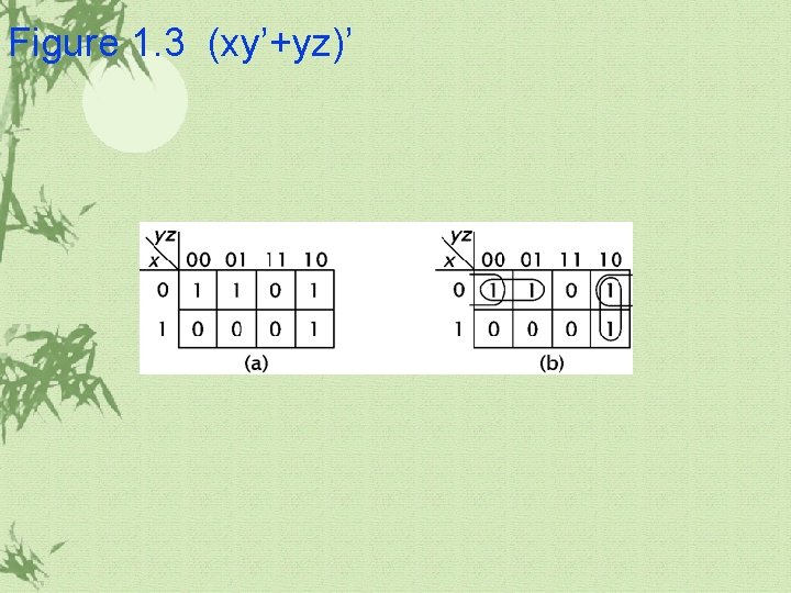
1. 1 Boolean Algebra(계속) De. Morgan’s Law It allows a digital designer to convert an AND function to an equivalent OR function and vice versa. ü (ab)’=a’+b’ ü (a+b)’=a’b’ ü Example: (xy’+yz)’=(xy’)’(yz)’=(x’+y)(y’+z’) =x’y’+x’z’+yy’+ yz’ = x’y’+x’z’+ yz’

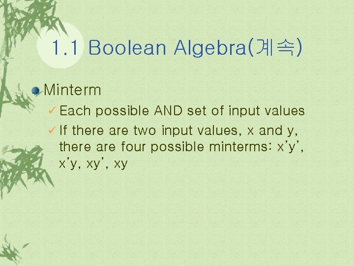
1. 1 Boolean Algebra(계속) Minterm ü Each possible AND set of input values ü If there are two input values, x and y, there are four possible minterms: x’y’, x’y, xy’, xy

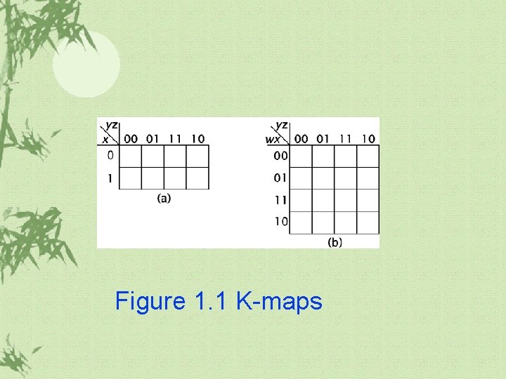
1. 1 Boolean Algebra(계속) K-map (Karnaugh-map) üA useful device for minimizing logic

Figure 1. 1 K-maps

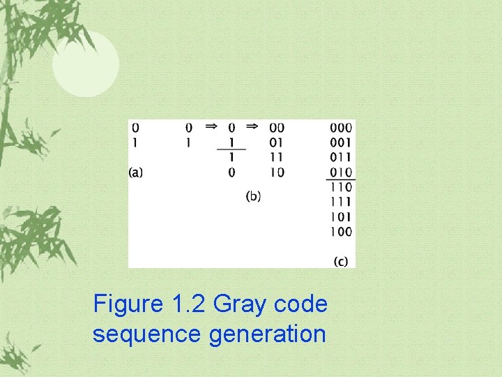
1. 1 Boolean Algebra(계속) K-map ü The ordering of K-map inputs: Gray code ü A Gray code is a reflected code.

Figure 1. 2 Gray code sequence generation

1. 1 Boolean Algebra(계속) Grouping on K-map ü Prime Implicants(PI) ü Essential Prime Implicants(EPI): groups which include cells that covered by only one group.

Figure 1. 3 (xy’+yz)’

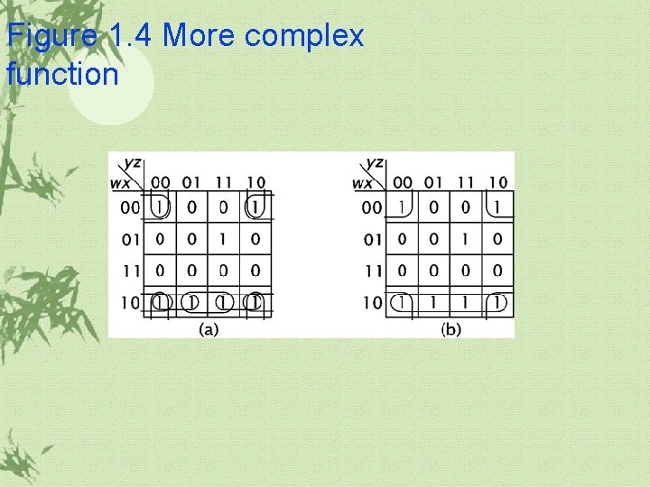
Figure 1. 4 More complex function

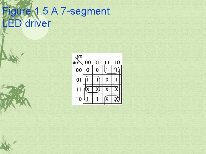
1. 1 Boolean Algebra(계속) Don’t care ü When some patterns of input values will never occur, it is called don’t care condition. ü We can treat the don’t care values as either 0 or 1, whichever makes it easier to group the minterms.

Figure 1. 5 A 7 -segment LED driver

1. 2 Basic Combinatorial Logic Gates: digital components that implement the logic functions. AND ü OR ü NOT ü NAND ü NOR ü XNOR ü

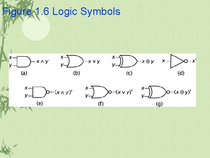
Figure 1. 6 Logic Symbols

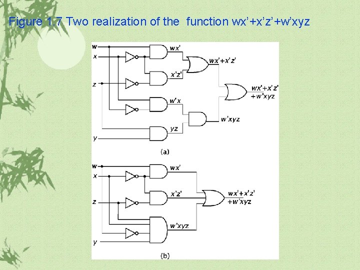
1. 2 Basic Combinatorial Logic(continued) The gates can be combined to realize more complex functions. There are some realization ways for a given complex functions depending on the conditions.

Figure 1. 7 Two realization of the function wx’+x’z’+w’xyz

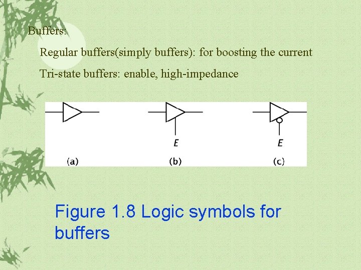
1. 2 Basic Combinatorial Logic(continued) Buffers: Buffers do not perform any operations on its input. ü Regular buffer: to boost the current of input to a higher level ü Tri-state buffer: it has a data input, just like the regular buffer, but also an enable input, E. ü If E is disable state, it produces a high impedance output.

Buffers: Regular buffers(simply buffers): for boosting the current Tri-state buffers: enable, high-impedance Figure 1. 8 Logic symbols for buffers

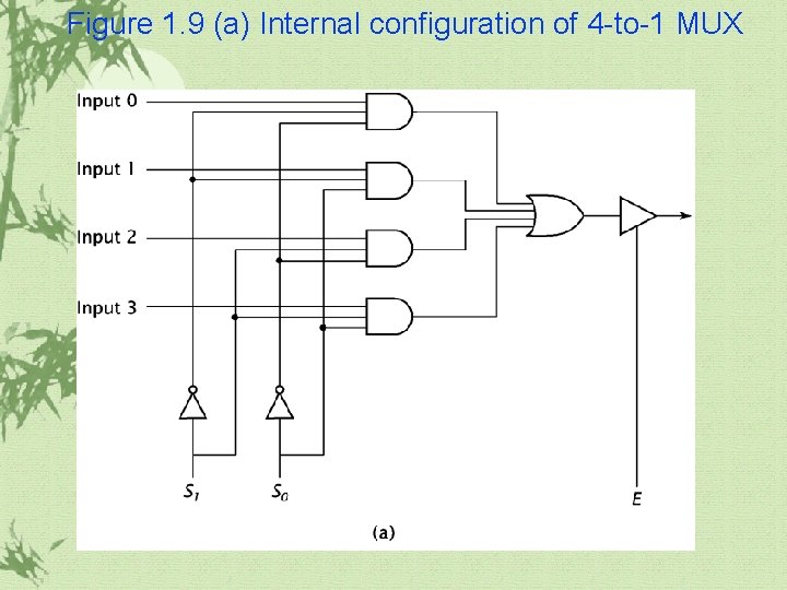
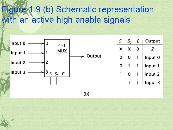
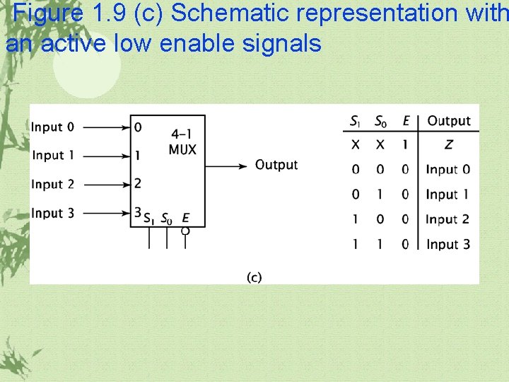
1. 3 More Complex Combinatorial Components Multiplexer(MUX) ü It chooses one of its data inputs and passes it through to its output. ü Select signals are needed for select a data input

Figure 1. 9 (a) Internal configuration of 4 -to-1 MUX

Figure 1. 9 (b) Schematic representation with an active high enable signals

Figure 1. 9 (c) Schematic representation with an active low enable signals

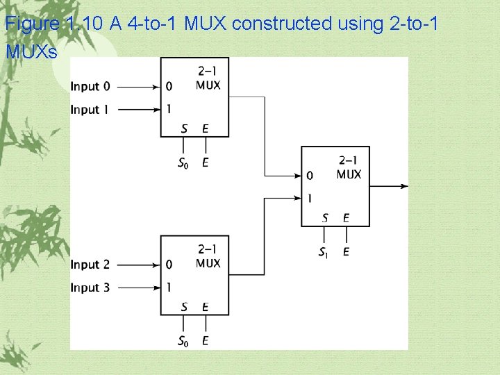
Figure 1. 10 A 4 -to-1 MUX constructed using 2 -to-1 MUXs

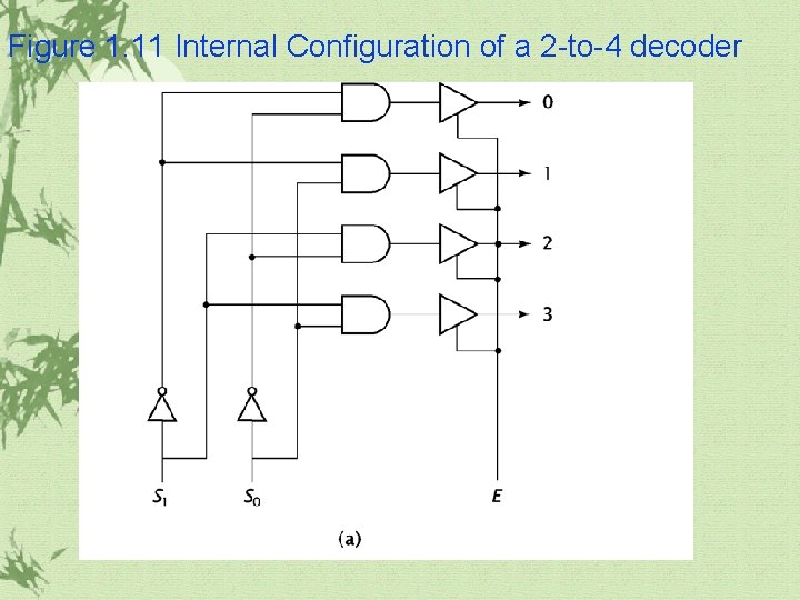
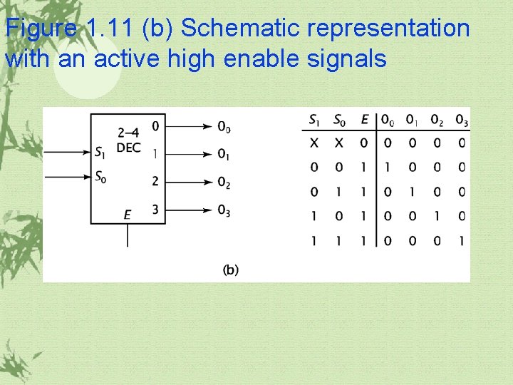
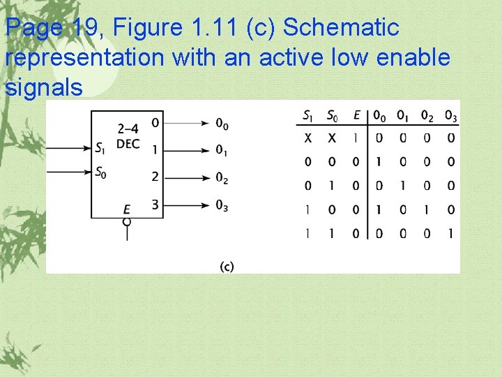
1. 3 More Complex Combinatorial Components(continued) Decoder ü It accepts a value and decodes it. ü It has n inputs and 2 n outputs, numbered from 0 to 2 n– 1.

Figure 1. 11 Internal Configuration of a 2 -to-4 decoder

Figure 1. 11 (b) Schematic representation with an active high enable signals

Page 19, Figure 1. 11 (c) Schematic representation with an active low enable signals

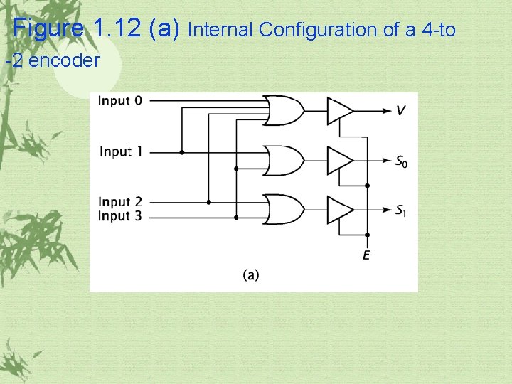
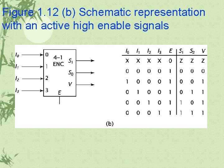
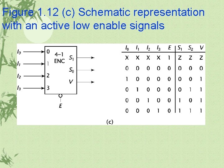
1. 3 More Complex Combinatorial Components(continued) Encoder ü It is the exact opposite of the decoder. ü It receives 2 n inputs and outputs an n-bit value corresponding to the input value.

Figure 1. 12 (a) Internal Configuration of a 4 -to -2 encoder

Figure 1. 12 (b) Schematic representation with an active high enable signals

Figure 1. 12 (c) Schematic representation with an active low enable signals

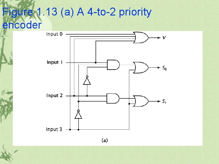
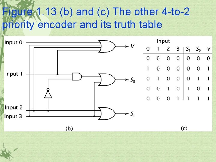
1. 3 More Complex Combinatorial Components(continued) Priority encoder ü The encoder works if zero or one inputs are active, but fails. ü A priority encoder works just like a regular encoder, with one exception, Whenever more than one input is active, the output is set to corresponding to the highest active input.

Figure 1. 13 (a) A 4 -to-2 priority encoder

Figure 1. 13 (b) and (c) The other 4 -to-2 priority encoder and its truth table

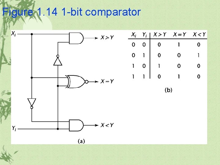
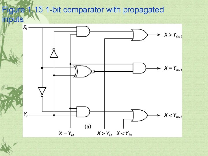
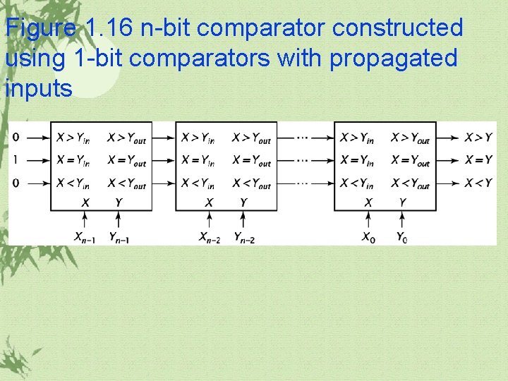
1. 3 More Complex Combinatorial Components(continued) Comparator ü It compares two n-bit binary values to determine which is greater, or if they are equal.

Figure 1. 14 1 -bit comparator

Figure 1. 15 1 -bit comparator with propagated inputs

Figure 1. 16 n-bit comparator constructed using 1 -bit comparators with propagated inputs

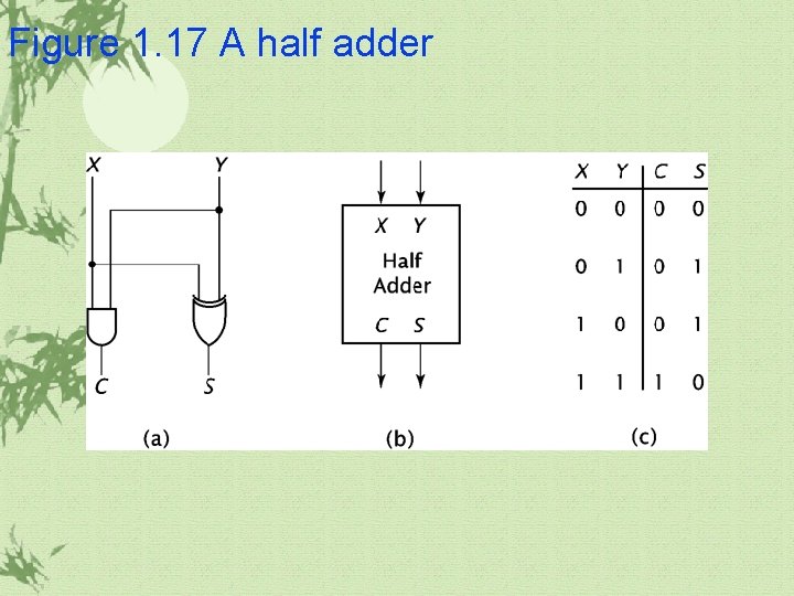
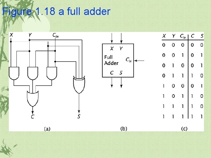
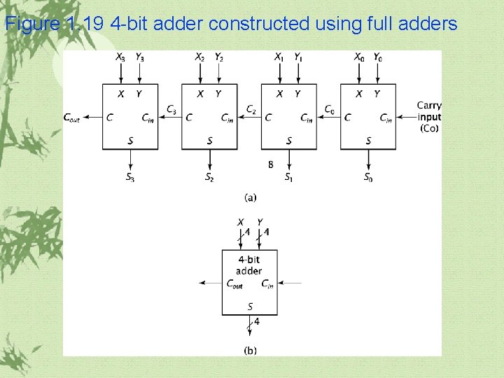
1. 3 More Complex Combinatorial Components(continued) Adder ü Adders are most commonly used, not only to perform addition, but also to perform subtraction, multiplication, and division. ü Half adder ü Full adder ü Ripple adder ü Carry lookahead addeer

Figure 1. 17 A half adder

Figure 1. 18 a full adder

Figure 1. 19 4 -bit adder constructed using full adders

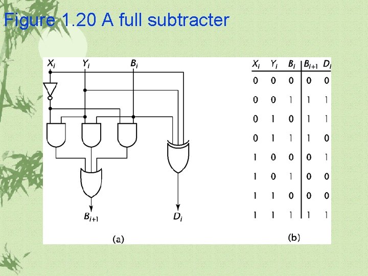
1. 3 More Complex Combinatorial Components(continued) Full subtracter üA full subtracter(Figure 1. 20) ü Two’s complement addition ü By doing this, a CPU may use a parallel adder for addition and subtraction.

Figure 1. 20 A full subtracter

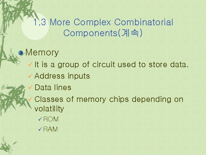
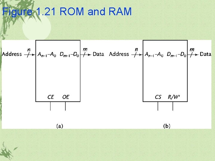
1. 3 More Complex Combinatorial Components(계속) Memory ü It is a group of circuit used to store data. ü Address inputs ü Data lines ü Classes of memory chips depending on volatility ü ROM ü RAM

Figure 1. 21 ROM and RAM

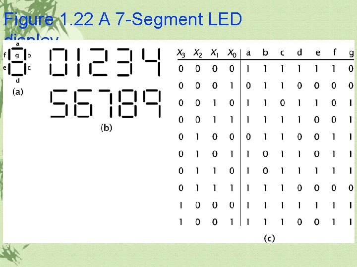
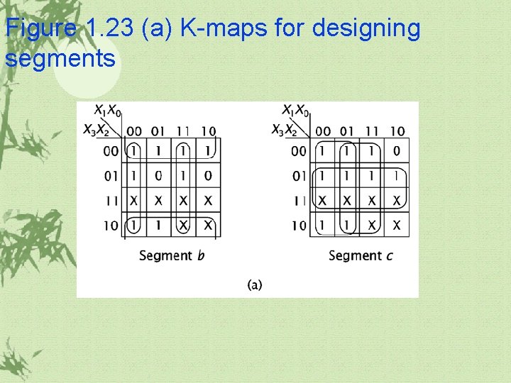
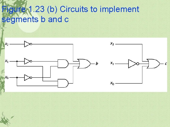
1. 4 Combinatorial Circuit Design BCD to 7 -Segment Decoder

Figure 1. 22 A 7 -Segment LED display

Figure 1. 23 (a) K-maps for designing segments

Figure 1. 23 (b) Circuits to implement segments b and c

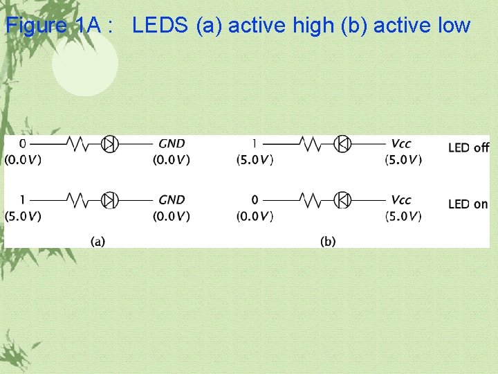
Figure 1 A : LEDS (a) active high (b) active low

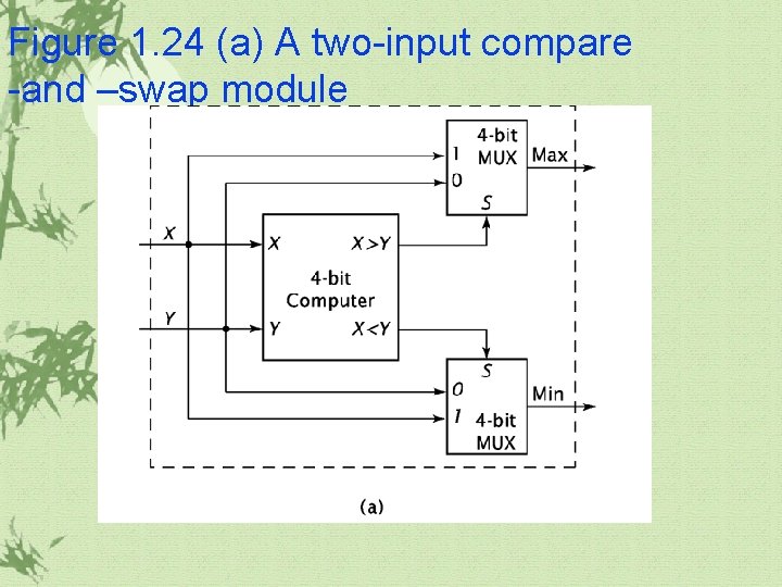
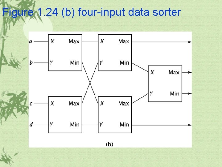
1. 4 Combinatorial Circuit Design(continued) A sorter

Figure 1. 24 (a) A two-input compare -and –swap module

Figure 1. 24 (b) four-input data sorter

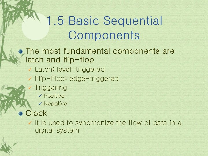
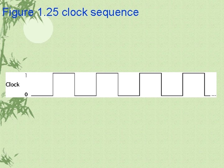
1. 5 Basic Sequential Components The most fundamental components are latch and flip-flop Latch: level-triggered ü Flip-Flop: edge-triggered ü Triggering ü Positive ü Negative ü Clock ü It is used to synchronize the flow of data in a digital system

Figure 1. 25 clock sequence

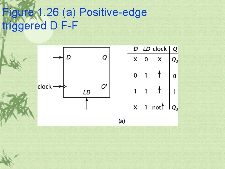
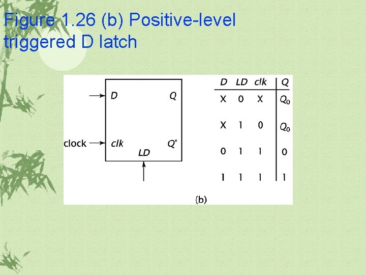
1. 5 Basic Sequential Components(continued) D latch and D F-F ü It has one input, D, and a clock input. ü The value of D becomes output, Q, after some delay. ü LD signal: It must be high as the clock changes from 0 to 1 in order for the data to be loaded into the F-F.

Figure 1. 26 (a) Positive-edge triggered D F-F

Figure 1. 26 (b) Positive-level triggered D latch

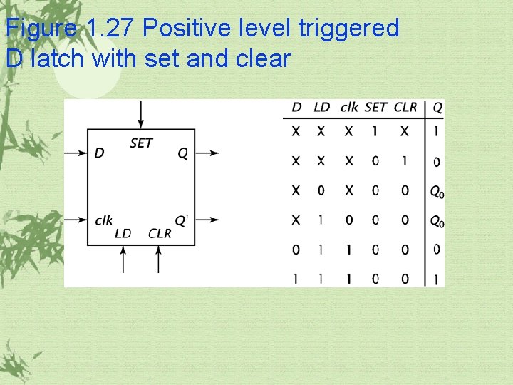
Figure 1. 27 Positive level triggered D latch with set and clear

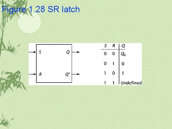
Figure 1. 28 SR latch

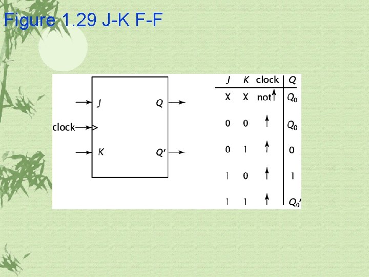
1. 5 Basic Sequential Components(continued) JK-FF ü It resolves the problem of undefined when SR=11

Figure 1. 29 J-K F-F

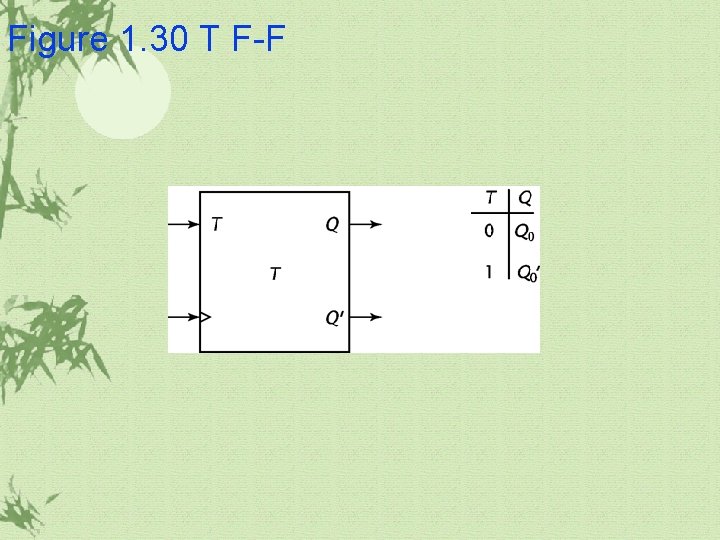
Figure 1. 30 T F-F

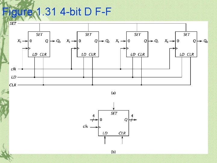
1. 5 Basic Sequential Components(continued) Flip-flops and latches may be combined in parallel to store data with more than one bit.

Figure 1. 31 4 -bit D F-F

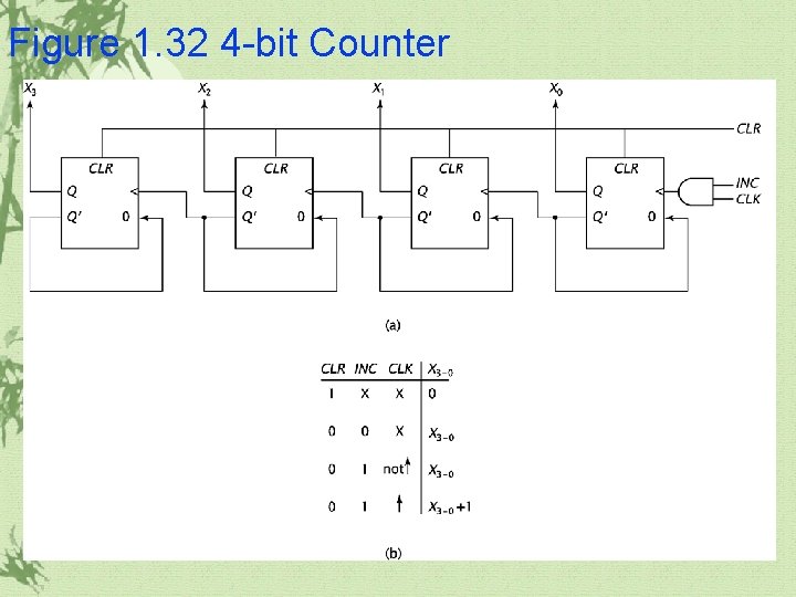
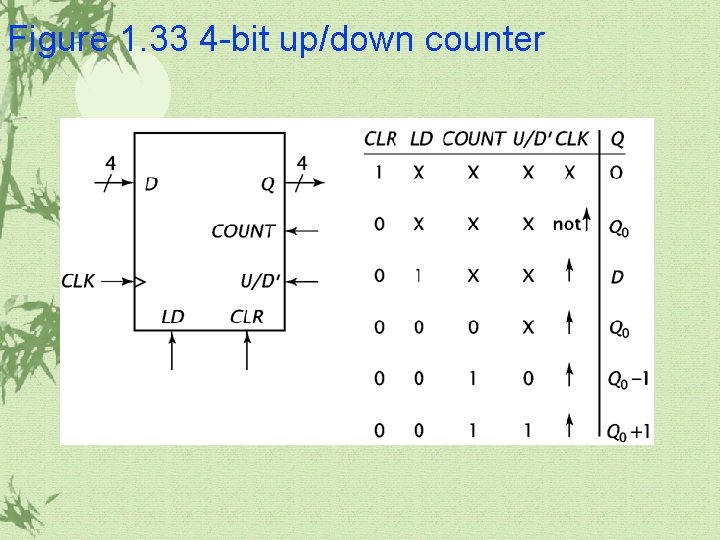
1. 6 More Complex Sequential Components Counters ü It stores a binary value and, when signaled to do so, arithmetically increases or decreases its value. ü Ripple counter ü Up/down counter

Figure 1. 32 4 -bit Counter

Figure 1. 33 4 -bit up/down counter

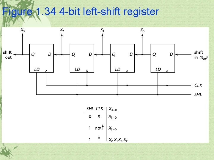
1. 6 More Complex Sequential Components Shift registers it can shift data one bit position to the right or left. ü It is particularly useful for certain hardware multipliers and dividers. ü

Figure 1. 34 4 -bit left-shift register

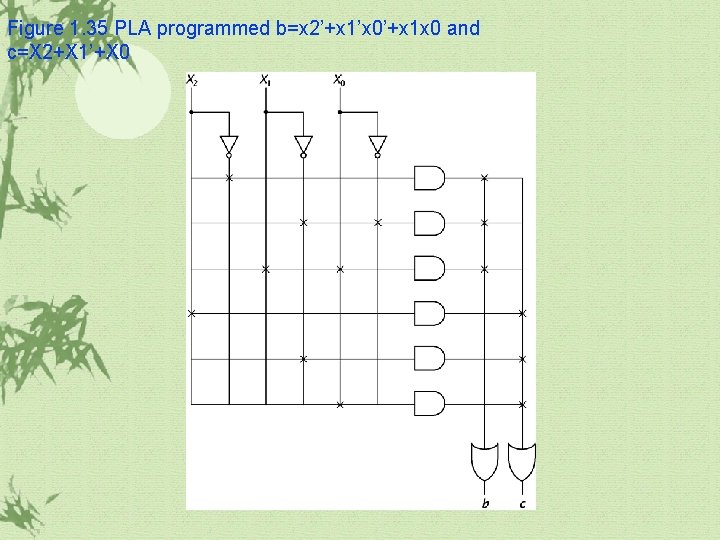
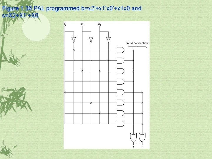
1. 7 Real World Example PLA PAL PLD FPGA

Figure 1. 35 PLA programmed b=x 2’+x 1’x 0’+x 1 x 0 and c=X 2+X 1’+X 0

Figure 1. 36 PAL programmed b=x 2’+x 1’x 0’+x 1 x 0 and c=X 2+X 1’+X 0