COMPUTER ORGANIZATION Topics Combinational design Flip Flops Counters

COMPUTER ORGANIZATION Topics: Combinational design, Flip. Flops, Counters, Registers

Combinational Circuits

Designing Combinational Circuits In general we have to do following steps: 1. Problem description 2. Input/output of the circuit 3. Define truth table 4. Simplification for each output 5. Draw the circuit

Decoder • Is a combinational circuit that converts binary information from n input lines to a maximum of 2 n unique output lines For example if the number of input is n=3 the number of output lines can be m=23. It is also known as 1 of 8 because one output line is selected out of 8 available lines: 3 to 8 decoder enable

Encoder • Encoder is a digital circuit that performs the inverse operation of a decoder • Generates a unique binary code from several input lines. • Generally encoders produce 2 -bit, 3 -bit or 4 -bit code. n bit encoder has 2 n input lines 2 bit encoder

2 -bit Priority Encoder • A priority encoder is an encoder circuit that includes priority function. • It means if two or more inputs are equal to 1 at the same time, the input having higher subscript number, considered as a higher priority. For example if D 3 is 1 regardless of the value of the other input lines the result of output is 3 which is 11. • If all inputs are 0, there is no valid input. For detecting this situation we considered a third output named V. V is equal to 0 when all input are 0 and is one for rest of the situations of TT.

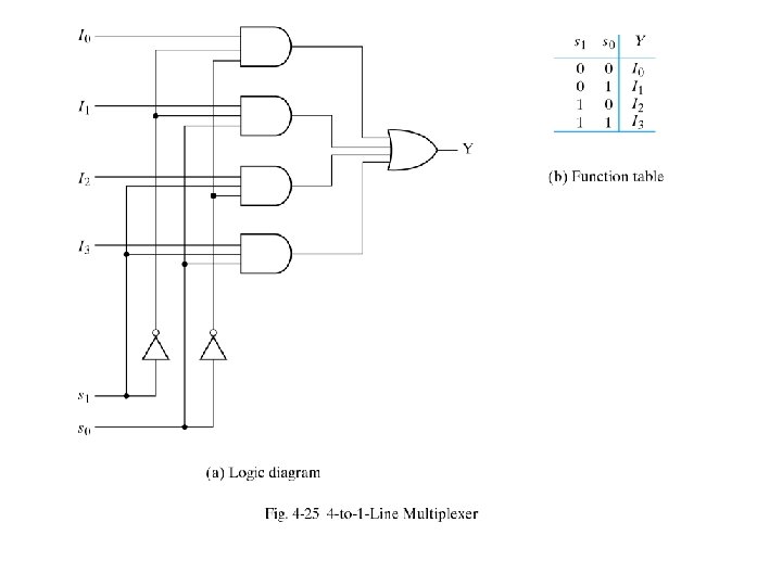
Multiplexer • It is a combinational circuit that selects binary information from one of the input lines and directs it to a single output line • Usually there are 2 n input lines and n selection lines whose bit combinations determine which input line is selected • For example for 2 -to-1 multiplexer if selection S is zero then I 0 has the path to output and if S is one I 1 has the path to output (see the next slide)

2 -to-1 multiplexer

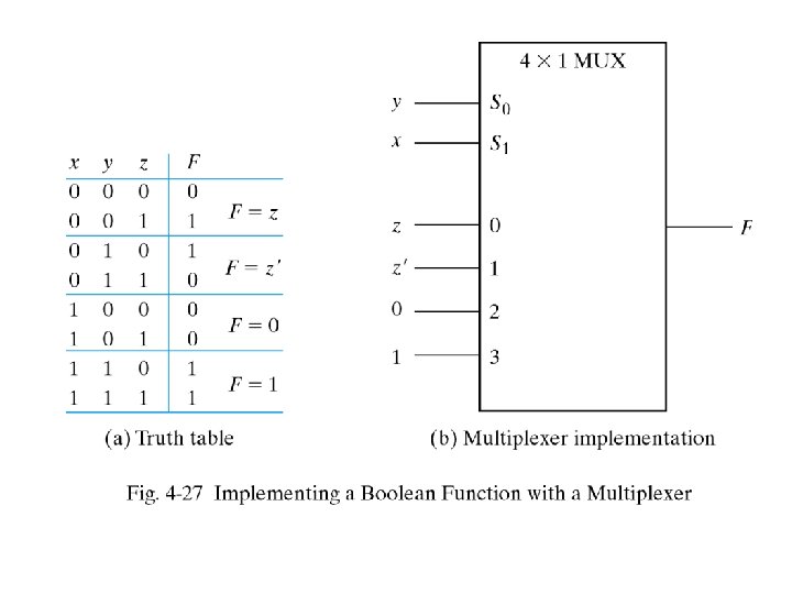
Boolean function Implementation • • Another method for implementing boolean function is using multiplexer For doing that assume boolean function has n variables. We have to use multiplexer with n-1 selection lines and 1 - first n-1 variables of function is used for data input 2 - the remaining single variable ( named z )is used for data input. Each data input can be z, z’, 1 or 0. From truth table we have to find the relation of F and z to be able to design input lines. For example : f(x, y, z) = ∑(1, 2, 6, 7)
")
F A, B, C, D = ∑(1, 3, 4, 11, 12, 13, 14, 15)

Three-State Gates • Three state gates exhibit three states instead of two states. The three states are: • high : 1 • Low : 0 • High impedance : In that state the output is disconnected which is equal to open circuit. In the other words in that state circuit has no logic significant. We can have AND or NAND treestate gates but the most common is three-state buffer gate

Three-state buffer C A Y -----------0 0 z 0 1 z 1 0 0 1 1 1

Sequential Circuits Inputs Combinational circuit Outputs Memory • The outputs of a sequential circuit depend on not only the inputs, but also the state, or the current contents of some memory • This makes things more difficult to understand, since the same inputs can yield different outputs, depending on what’s stored in memory • The memory contents can also change as the circuit runs • We’ll some need new techniques for analyzing and designing sequential circuits 19

Examples of Sequential Devices • Many real-life devices are sequential in nature: – Combination locks open if you enter numbers in the right order – Elevators move up or down and open or close depending on the buttons that are pressed on different floors and in the elevator itself – Traffic lights may switch from red to green depending on whether or not a car is waiting at the intersection 20

LOGIC CIRCUITS Logic circuits are classified into two groups: Combinational logic circuits Logic gates make decisions Basic building blocks include: Sequential logic circuits Basic building blocks include FLIP-FLOPS: Flip Flops have memory

FLIP-FLOPS • Memory device capable of storing one bit • Memory means circuit remains in one state after condition that caused the state is removed. • Two outputs designated Q and Q-Not that are always opposite or complimentary. • When referring to the state of a flip flop, referring to the state of the Q output.

FLIP-FLOPS SET Symbol • To SET a flip flop means to make Q =1 RESET Truth Table • To RESET a flip flop means to make Q = 0

R-S FLIP-FLOP Active-High

CLOCKED R-S FLIP-FLOP Set S Reset R Set FF Q Q ASYNCHRONOUS Outputs of logic circuit can change state anytime one or more input changes S Clock Reset FF Q CLK R Q SYNCHRONOUS Clock signal determines exact time at which any output can change state

TRIGGERING OF FLIP-FLOPS • Level-triggering is the transfer of data from input to output of a flip-flop anytime the clock pulse is proper voltage level. • Edge-triggering is the transfer of data from input to output of a flip-flop on the rising edge (L-to-H) or falling edge (Hto-L) of the clock pulse. Edge triggering may be either positive-edge (L-to-H) or negative-edge (H-to-L). NGT-Negative Going Transition PGT-Positive Going Transition Positive-edge triggering Negative-edge triggering H L time Level triggering

CLOCKED R-S FLIP-FLOP Symbols: Set Clock Reset S FF Q Normal CLK R Q Complementary Truth Table: Mode of operation Clk Hold Reset Set Prohibited S + pulse NOTE: Active-High inputs Inputs R 0 0 0 1 1 Outputs Q Q’ no change 0 1 1 0 0 0

Excitation Table • The excitation table tells the designer the minimum inputs that are necessary to generate a particular next state when the current state is known • They are similar to truth tables and state tables, but rearrange the data so that the current state and next state are next to each other on the left-hand side of the table, and the inputs needed to make that state change happen are shown on the right side of the table • This is the same information that’s given in the transition table, but presented “backwards” 28

Excitation Table for T Flip Flop Transition Table Excitation Table Rearranging rows and/or columns… Tells how inputs affect output Tells what input is needed to achieve desired output transition In the end, they are the same table, just rearranged… 29

Excitation Table for D Flip Flop Transition Table Excitation Table Rearranging rows and/or columns… Tells how inputs affect output Tells what input is needed to achieve desired output transition In the end, they are the same table, just rearranged… 30

Excitation Table for JK Flip Flop Rearranging rows and/or columns… Tells what input is needed to achieve desired output transition Tells how inputs affect output Do you see why the X’s? In the end, they are the same table, just rearranged… 31

Excitation Table for JK Flip Flop Rearranging rows and/or columns… Tells what input is needed to achieve desired output transition Tells how inputs affect output Do you see why the X’s? In the end, they are the same table, just rearranged… 32

Excitation Table for JK Flip Flop Rearranging rows and/or columns… Tells what input is needed to achieve desired output transition Tells how inputs affect output Do you see why the X’s? In the end, they are the same table, just rearranged… 33

Excitation Table for SR Flip Flop Rearranging rows and/or columns… Tells what input is needed to achieve desired output transition Tells how inputs affect output In the end, they are the same table, just rearranged… 34

Excitation Table • The excitation table tells the designer the minimum inputs that are necessary to generate a particular next state when the current state is known • They are similar to truth tables and state tables, but rearrange the data so that the current state and next state are next to each other on the left-hand side of the table, and the inputs needed to make that state change happen are shown on the right side of the table • This is the same information that’s given in the transition table, but presented “backwards” 35

Excitation Table for T Flip Flop Transition Table Excitation Table Rearranging rows and/or columns… Tells how inputs affect output Tells what input is needed to achieve desired output transition In the end, they are the same table, just rearranged… 36

Excitation Table for D Flip Flop Transition Table Excitation Table Rearranging rows and/or columns… Tells how inputs affect output Tells what input is needed to achieve desired output transition In the end, they are the same table, just rearranged… 37

Excitation Table for JK Flip Flop Rearranging rows and/or columns… Tells what input is needed to achieve desired output transition Tells how inputs affect output Do you see why the X’s? In the end, they are the same table, just rearranged… 38

Excitation Table for JK Flip Flop Rearranging rows and/or columns… Tells what input is needed to achieve desired output transition Tells how inputs affect output Do you see why the X’s? In the end, they are the same table, just rearranged… 39

Excitation Table for JK Flip Flop Rearranging rows and/or columns… Tells what input is needed to achieve desired output transition Tells how inputs affect output Do you see why the X’s? In the end, they are the same table, just rearranged… 40

Excitation Table for SR Flip Flop Rearranging rows and/or columns… Tells what input is needed to achieve desired output transition Tells how inputs affect output In the end, they are the same table, just rearranged… 41

Registers • A register is a collection of flip-flops that act as an extension of a flip-flop which can store multiple bits • It has two basic functions: Data Storage and Data Movement • A shift register provides the data movement function where it is capable of shifting their binary contents in one or both directions (shifting data to the left or right) – It “shifts” its output once every clock cycle 42

A Basic Register • Basic registers are easy to build. We can store multiple bits just by putting a bunch of flip-flops together! • A 4 -bit register with its internal implementation is as shown below – This register uses D flip-flops – All the flip-flops share a common CLK and CLR signal Prepared by K. T. NG 43

Shift Registers • A shift register "shifts" its output once every clock cycle Q 0(t+1) = SI Q 1(t+1) = Q 0(t) Q 2(t+1) = Q 1(t) Q 3(t+1) = Q 2(t) • • SI is an input that supplies a new bit to shift "into" the register For example, if on some positive clock edge we have: SI = 1 Q 0 -Q 3 = 0110 then the next state will be: Q 0 -Q 3 = 1011 • The current Q 3 (0 in this example) will be lost on the next cycle 44

Basic Shift Register Operation • Some basic data movements are illustrated here: Data in Data out Serial in/shift right/serial out Data in Serial in/shift left/serial out Parallel in/serial out Data in Data out Serial in/parallel out Data out Parallel in/parallel out Rotate right Rotate left 45

Serial Transfer vs. Parallel Transfer • Serial transfer – Information is transferred one bit at a time – Shifts the bits out of the source register into the destination register • Parallel transfer: – All the bits of the register are transferred at the same time • For example: – Older printers use parallel data transfer – USB devices use serial data transfer 46

Parallel Data Transfer Parallel data transfer moves data from one register to another at one time Reg. A Reg. B clock When clock occurs, all bits of A are copied to B 47

Counters • A counter is a a specific type of sequential circuit that goes through a prescribed sequence of states each time an input clock pulse makes an active transition Count Clock Counter Load an initial value, reset to starting count, etc. Preparedinputs by K. T. NG optional The state, or the flipflop values themselves, serves as the “output” May also enable count, select direction, etc. 48
 counters – The flip-flop output transition serves as")
Categories of Counters 1. Asynchronous (ripple) counters – The flip-flop output transition serves as a source for triggering other flip-flops – No common clock pulse (not synchronous) HIGH Q 0 J 0 CLK C K 0 Q 1 J 1 C Q 0 K 1 Q 2 J 2 C Q 1 K 2 An example of a 3 -bit asynchronous counter which use J-K flipflops in the toggle mode 49
 1. Synchronous counters: – The CLK inputs of all")
Categories of Counters (Cont. ) 1. Synchronous counters: – The CLK inputs of all flip-flops receive a common clock – Synchronous counters overcome the disadvantage of accumulated propagation delays, but generally they require more HIGH Q circuitry to control states changes QQ 0 J 0 C K 0 Q 0 J 1 Q 1 1 J 2 C C K 1 K 2 Prepared by K. T. NG CLK 0 Q 2 50

Counting in Binary • The binary counting sequence is shown on the right • Look at the column labelled Q 0. It reads 0, 1, etc. If this were drawn as a timing diagram, it would look like a clock. Assume that this clock has period T • Now look at the column labelled Q 1. It reads 0, 0, 1, 1, 0, 0, 1, 1. It looks like a clock too! However, it stays 0 twice as long, then 1 twice as long. In fact, it looks like a clock that has a period of 2 T • Now look at the column labelled Q 2. It reads 0, 0, 1, 1, 1, 1. Again, this looks like a clock, except it's going twice as slow! It has a period of 4 T! 51

The Timing Diagram that Shows How the Counter Behaves “ 0” “ 1” “ 2” “ 3” “ 4” Q 0 0 1 0 Q 1 0 0 1 1 0 0 “ 5” “ 6” “ 7” 1 0 0 1 1 1 CLK Q 2 Repeats → Note: assume the flip-flops using are positive edge trigger 52
 Counter • Starting with three positive edge triggered")
Build a 3 -bit Asynchronous (Ripple) Counter • Starting with three positive edge triggered J-K flipflops connected in "toggle" mode, we need to determine how to connect the clock inputs in such a way so that each succeeding bit toggles when the bit before it transitions from 1 to 0 • The Q outputs of each flip-flop will serve as the respective binary bits of the final, three-bit count 53
 Counter (Cont. ) • If we look at")
Build a 3 -bit Asynchronous (Ripple) Counter (Cont. ) • If we look at the previous timing diagram, we really want Q 1 to toggle on negative edges of Q 0 • However, the JK flip-flop in "toggle" mode will toggle on positive edges. How can we solve this problem? • Answer: Since the Q' output will always be the exact opposite state of the Q output on a J-K flip-flop. To toggle on negative edges of Q 0 is equivalent to toggling on the positive edges of Q 0', which is the negation of Q 0 In other words, each time the Q 0 output of a flip-flop transitions from 1 to 0, the Q 0' output of the same flip-flop will transition from 0 to 1, providing the positive-going clock pulse we would need to toggle a positive-edge triggered flip-flop at the right moment • Similarly, we want Q 2 to toggle on negative edges of Q 1 and thus we have: 54
 Counter (Cont. ) • The following is a")
Build a 3 -bit Asynchronous (Ripple) Counter (Cont. ) • The following is a three-bit asynchronous binary counter and its timing diagram for one cycle Prepared by K. T. NG 55
 Counter (Cont. ) • To expand the idea")
Build a 3 -bit Asynchronous (Ripple) Counter (Cont. ) • To expand the idea above, the following is the three-bit asynchronous binary counter that using negative edge triggered J-K flip flop and its timing diagram for one cycle: 56
 Counter (Cont. ) • An asynchronous toggle flip-flop")
Build a 3 -bit Asynchronous (Ripple) Counter (Cont. ) • An asynchronous toggle flip-flop can also be built using an edge-triggered D flip-flop • It is common practice to make a D flip-flop act as a T flip-flop by connecting its D input fed from its own inverted output. Then each pulse to the clock input will load the D input from the opposite state at its own inverted output positive edge trigger T flip-flop formed by D flip-flop negative edge trigger T flip-flop formed by D flip-flop 57
 Counter (Cont. ) • Thus, the following is")
Build a 3 -bit Asynchronous (Ripple) Counter (Cont. ) • Thus, the following is the three-bit asynchronous binary counter that using negative edge triggered D type flip flop and its timing diagram for one cycle: Prepared by K. T. NG 58
- Slides: 58