Computer Organization Motivation Computer Design as an application

![Bussing Strategies Example Register Transfer for Single Bus Design Instruction Interpretation for "ADD Mem[X]" Bussing Strategies Example Register Transfer for Single Bus Design Instruction Interpretation for "ADD Mem[X]"](https://slidetodoc.com/presentation_image_h/1d8b63054987621a1d48b8fea5e3d563/image-25.jpg)
![Bussing Strategies Multiple Busses Instruction Interpretation for "ADD Mem[X]" Fetch Operand Cycle 1: IR<operand Bussing Strategies Multiple Busses Instruction Interpretation for "ADD Mem[X]" Fetch Operand Cycle 1: IR<operand](https://slidetodoc.com/presentation_image_h/1d8b63054987621a1d48b8fea5e3d563/image-27.jpg)
- Slides: 47

Computer Organization

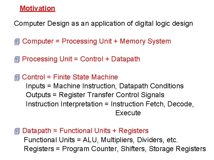
Motivation Computer Design as an application of digital logic design Computer = Processing Unit + Memory System Processing Unit = Control + Datapath Control = Finite State Machine Inputs = Machine Instruction, Datapath Conditions Outputs = Register Transfer Control Signals Instruction Interpretation = Instruction Fetch, Decode, Execute Datapath = Functional Units + Registers Functional Units = ALU, Multipliers, Dividers, etc. Registers = Program Counter, Shifters, Storage Registers

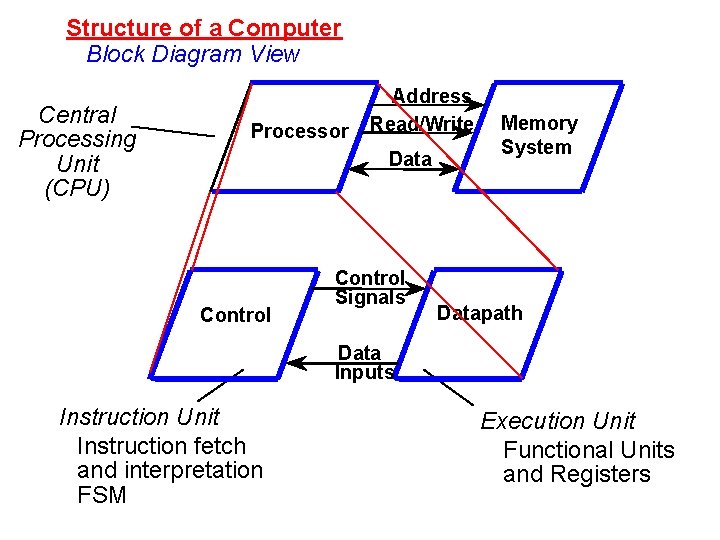
Structure of a Computer Block Diagram View Central Processing Unit (CPU) Processor Address Read/Write Data Control Signals Memory System Datapath Data Inputs Instruction Unit Instruction fetch and interpretation FSM Execution Unit Functional Units and Registers

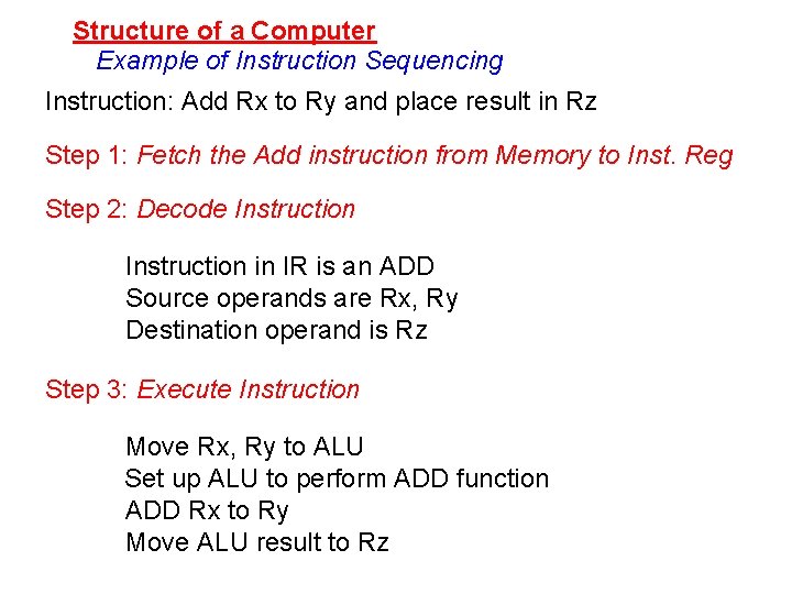
Structure of a Computer Example of Instruction Sequencing Instruction: Add Rx to Ry and place result in Rz Step 1: Fetch the Add instruction from Memory to Inst. Reg Step 2: Decode Instruction in IR is an ADD Source operands are Rx, Ry Destination operand is Rz Step 3: Execute Instruction Move Rx, Ry to ALU Set up ALU to perform ADD function ADD Rx to Ry Move ALU result to Rz

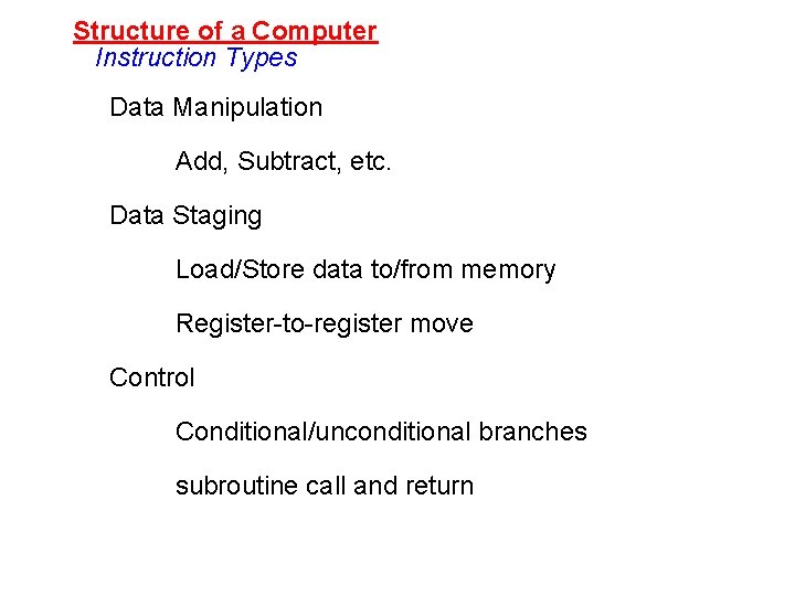
Structure of a Computer Instruction Types Data Manipulation Add, Subtract, etc. Data Staging Load/Store data to/from memory Register-to-register move Control Conditional/unconditional branches subroutine call and return

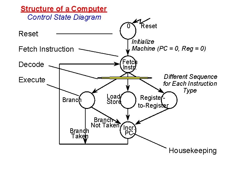
Structure of a Computer Control State Diagram 0 Reset Initialize Machine (PC = 0, Reg = 0) Fetch Instruction Fetch Instr. Decode Execute Branch Load/ Store Different Sequence for Each Instruction Type Registerto-Register Branch Not Taken Incr. Branch PC Taken Housekeeping

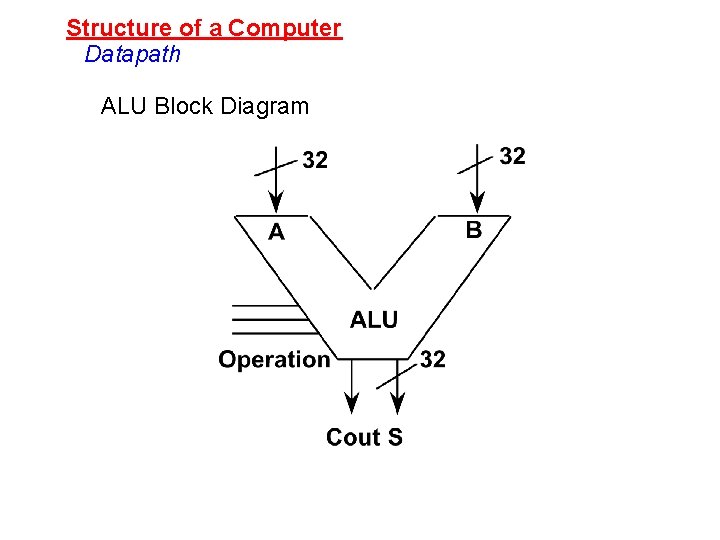
Structure of a Computer Datapath ALU Block Diagram

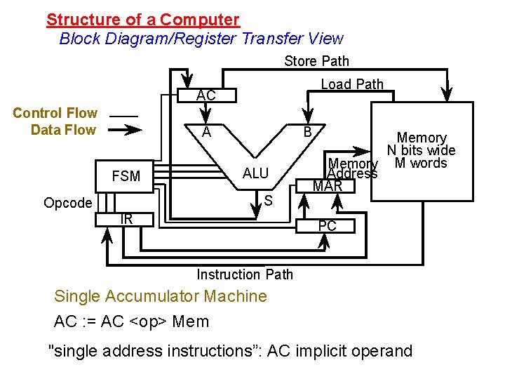
Structure of a Computer Block Diagram/Register Transfer View Store Path Load Path AC Control Flow Data Flow A FSM B ALU S Opcode IR Memory N bits wide Memory M words Address MAR PC Instruction Path Single Accumulator Machine AC : = AC <op> Mem "single address instructions”: AC implicit operand

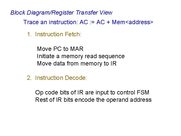
Block Diagram/Register Transfer View Trace an instruction: AC : = AC + Mem<address> 1. Instruction Fetch: Move PC to MAR Initiate a memory read sequence Move data from memory to IR 2. Instruction Decode: Op code bits of IR are input to control FSM Rest of IR bits encode the operand address

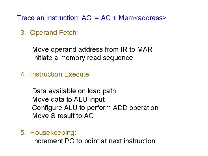
Trace an instruction: AC : = AC + Mem<address> 3. Operand Fetch: Move operand address from IR to MAR Initiate a memory read sequence 4. Instruction Execute: Data available on load path Move data to ALU input Configure ALU to perform ADD operation Move S result to AC 5. Housekeeping: Increment PC to point at next instruction

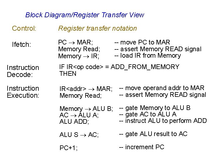
Block Diagram/Register Transfer View Control: Register transfer notation Ifetch: PC MAR; Memory Read; Memory IR; -- move PC to MAR -- assert Memory READ signal -- load IR from Memory Instruction Decode: IF IR<op code> = ADD_FROM_MEMORY THEN Instruction Execution: IR<addr> MAR; Memory Read; -- move operand addr to MAR -- assert Memory READ signal Memory ALU B; -- gate Memory to ALU B -- gate AC to ALU A AC ALU A; -- instruct ALU to perform ADD ALU ADD; ALU S AC; -- gate ALU result to AC PC+1; -- increment PC

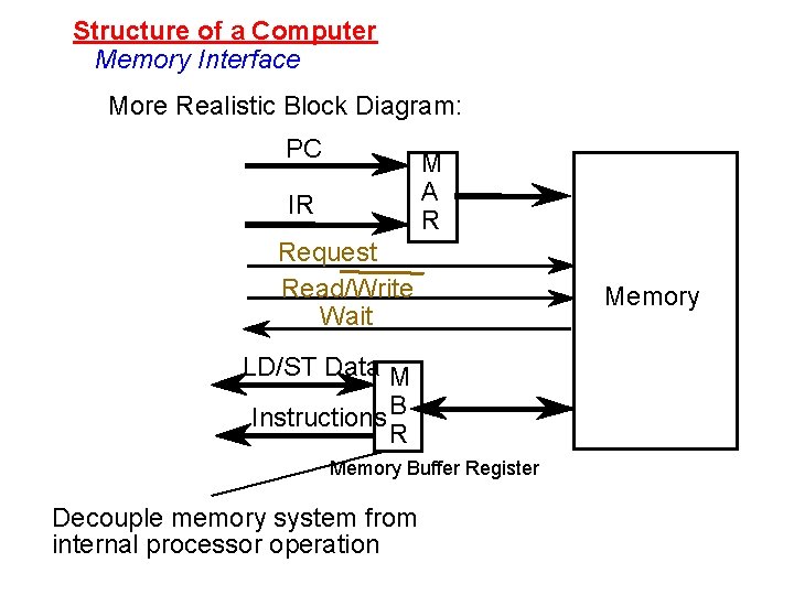
Structure of a Computer Memory Interface More Realistic Block Diagram: PC M A R IR Request Read/Write Wait LD/ST Data M Instructions B R Memory Buffer Register Decouple memory system from internal processor operation Memory

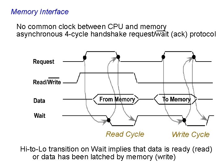
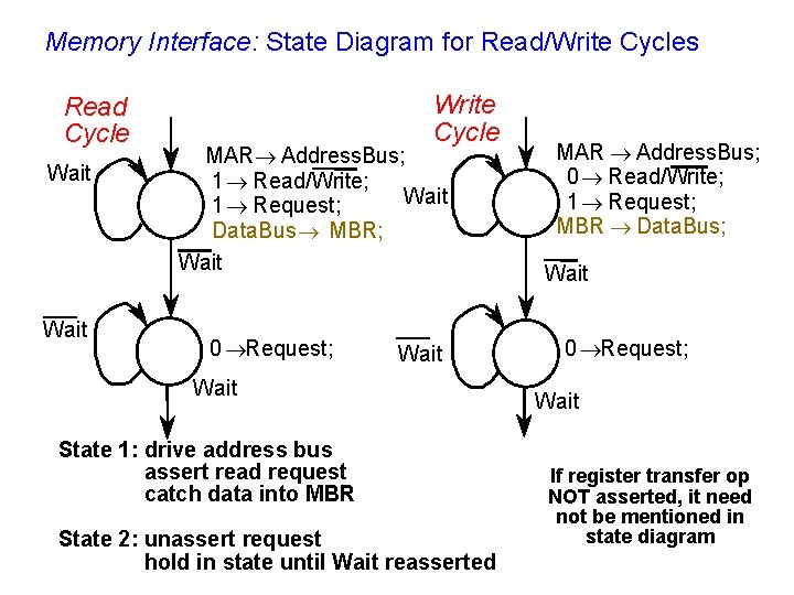
Memory Interface No common clock between CPU and memory asynchronous 4 -cycle handshake request/wait (ack) protocol Read Cycle Write Cycle Hi-to-Lo transition on Wait implies that data is ready (read) or data has been latched by memory (write)

Memory Interface: State Diagram for Read/Write Cycles Read Cycle Wait Write Cycle MAR Address. Bus; 1 Read/Write; Wait 1 Request; Data. Bus MBR; Wait 0 Request; Wait State 1: drive address bus assert read request catch data into MBR State 2: unassert request hold in state until Wait reasserted MAR Address. Bus; 0 Read/Write; 1 Request; MBR Data. Bus; Wait 0 Request; Wait If register transfer op NOT asserted, it need not be mentioned in state diagram

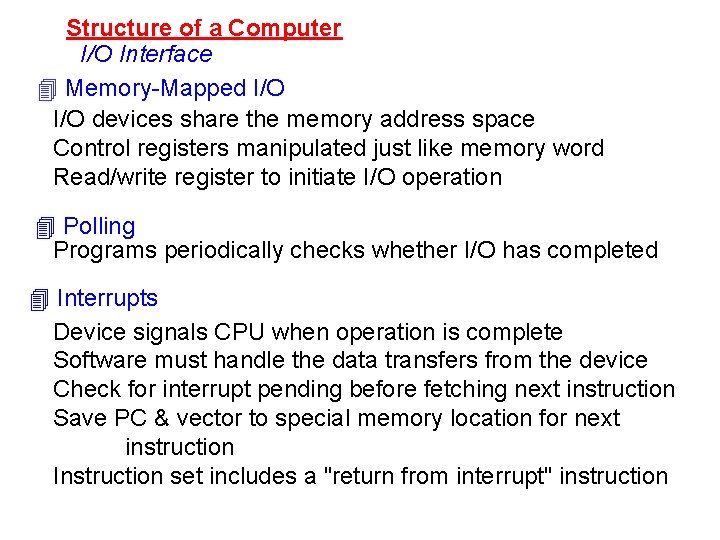
Structure of a Computer I/O Interface Memory-Mapped I/O devices share the memory address space Control registers manipulated just like memory word Read/write register to initiate I/O operation Polling Programs periodically checks whether I/O has completed Interrupts Device signals CPU when operation is complete Software must handle the data transfers from the device Check for interrupt pending before fetching next instruction Save PC & vector to special memory location for next instruction Instruction set includes a "return from interrupt" instruction

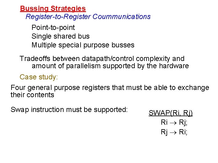
Bussing Strategies Register-to-Register Coummunications Point-to-point Single shared bus Multiple special purpose busses Tradeoffs between datapath/control complexity and amount of parallelism supported by the hardware Case study: Four general purpose registers that must be able to exchange their contents Swap instruction must be supported: SWAP(Ri, Rj) Ri Rj; Rj Ri;

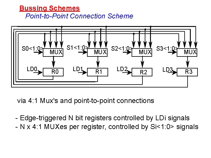
Bussing Schemes Point-to-Point Connection Scheme S 0<1: 0> LD 0 MUX R 0 S 1<1: 0> LD 1 MUX R 1 S 2<1: 0> LD 2 MUX R 2 S 3<1: 0> LD 3 MUX R 3 via 4: 1 Mux's and point-to-point connections - Edge-triggered N bit registers controlled by LDi signals - N x 4: 1 MUXes per register, controlled by Si<1: 0> signals

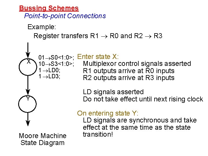
Bussing Schemes Point-to-point Connections Example: Register transfers R 1 R 0 and R 2 R 3 X 01 S 0<1: 0>; 10 S 3<1: 0>; 1 LD 0; 1 LD 3; Y Moore Machine State Diagram Enter state X: Multiplexor control signals asserted R 1 outputs arrive at R 0 inputs R 2 outputs arrive at R 3 inputs LD signals asserted Do not take effect until next rising clock On entering state Y: LD signals are synchronous and take effect at the same time as the state transition!

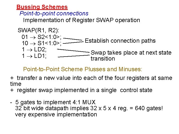
Bussing Schemes Point-to-point connections Implementation of Register SWAP operation SWAP(R 1, R 2): 01 S 2<1: 0>; 10 S 1<1: 0>; 1 LD 2; 1 LD 1; Establish connection paths Swap takes place at next state transition Point-to-Point Scheme Plusses and Minuses: + transfer a new value into each of the four registers at same time + register swap implemented in a single control state - 5 gates to implement 4: 1 MUX 32 bit wide datapath implies 32 x 5 x 4 reg. = 640 gates! very expensive implementation

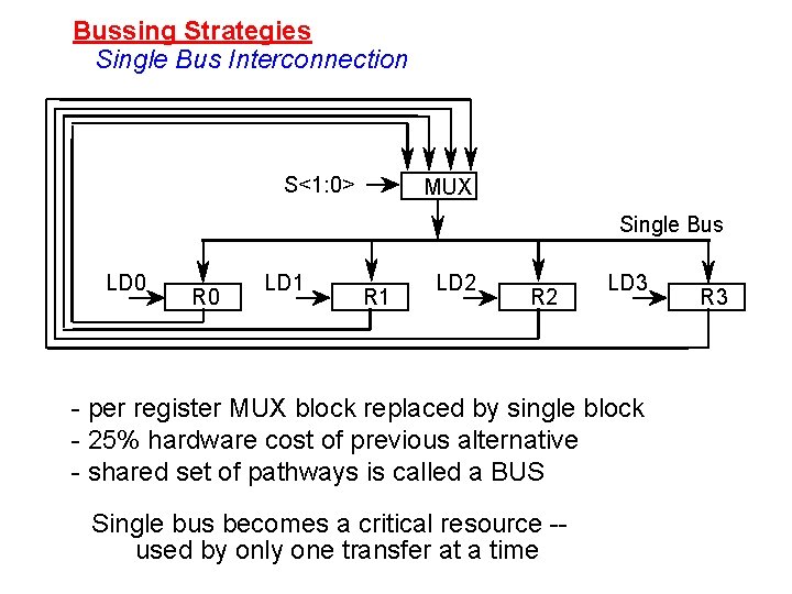
Bussing Strategies Single Bus Interconnection S<1: 0> MUX Single Bus LD 0 R 0 LD 1 R 1 LD 2 R 2 LD 3 - per register MUX block replaced by single block - 25% hardware cost of previous alternative - shared set of pathways is called a BUS Single bus becomes a critical resource -used by only one transfer at a time R 3

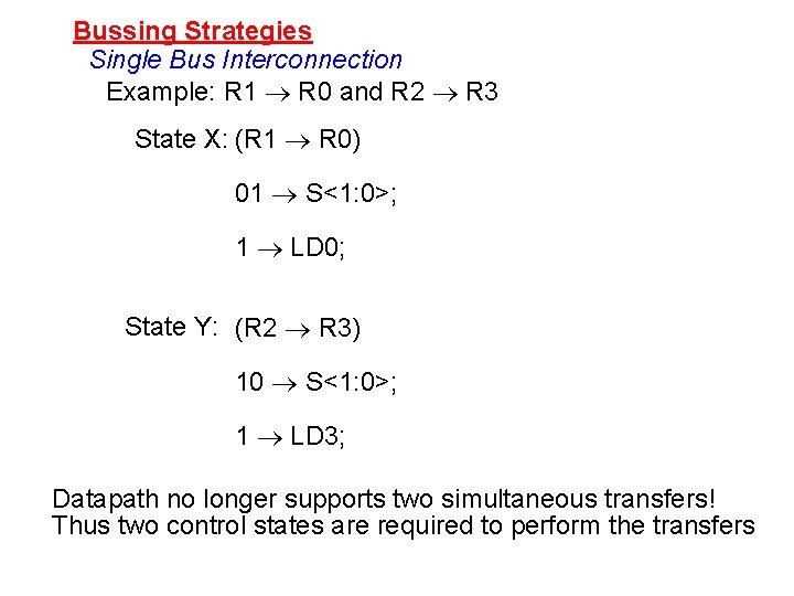
Bussing Strategies Single Bus Interconnection Example: R 1 R 0 and R 2 R 3 State X: (R 1 R 0) 01 S<1: 0>; 1 LD 0; State Y: (R 2 R 3) 10 S<1: 0>; 1 LD 3; Datapath no longer supports two simultaneous transfers! Thus two control states are required to perform the transfers

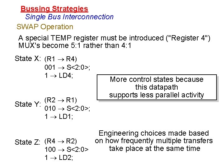
Bussing Strategies Single Bus Interconnection SWAP Operation A special TEMP register must be introduced ("Register 4") MUX's become 5: 1 rather than 4: 1 State X: (R 1 R 4) 001 S<2: 0>; 1 LD 4; State Y: (R 2 R 1) 010 S<2: 0>; 1 LD 1; More control states because this datapath supports less parallel activity Engineering choices made based on how frequently multiple transfers State Z: (R 4 R 2) take place at the same time 100 S<2: 0> 1 LD 2;

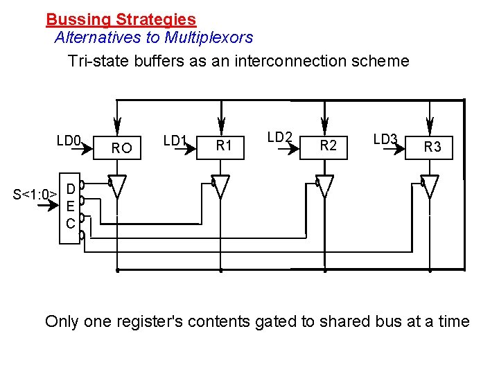
Bussing Strategies Alternatives to Multiplexors Tri-state buffers as an interconnection scheme LD 0 RO LD 1 R 1 LD 2 R 2 LD 3 R 3 S<1: 0> D E C Only one register's contents gated to shared bus at a time

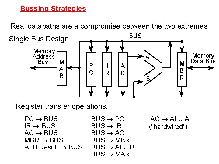
Bussing Strategies Real datapaths are a compromise between the two extremes BUS Single Bus Design Memory Address Bus M A R A P C I R A C B M B R Register transfer operations: PC BUS IR BUS AC BUS MBR BUS ALU Result BUS PC BUS IR BUS AC BUS MBR BUS ALU B BUS MAR AC ALU A ("hardwired") Memory Data Bus
![Bussing Strategies Example Register Transfer for Single Bus Design Instruction Interpretation for ADD MemX Bussing Strategies Example Register Transfer for Single Bus Design Instruction Interpretation for "ADD Mem[X]"](https://slidetodoc.com/presentation_image_h/1d8b63054987621a1d48b8fea5e3d563/image-25.jpg)
Bussing Strategies Example Register Transfer for Single Bus Design Instruction Interpretation for "ADD Mem[X]" Fetch Operand Cycle 1: IR<operand address> BUS; BUS MAR; Cycle 2: Memory Read; Databus MBR; Perform ADD Cycle 3: Write Result Cycle 4: MBR BUS; BUS ALU B; AC ALU A; ADD; ALU Result BUS; BUS AC; Requires latch for ALU Result

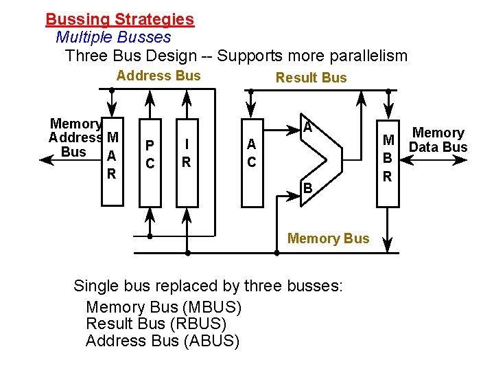
Bussing Strategies Multiple Busses Three Bus Design -- Supports more parallelism Address Bus Memory Address M Bus A R Result Bus A P C I R A C B Memory Bus Single bus replaced by three busses: Memory Bus (MBUS) Result Bus (RBUS) Address Bus (ABUS) M B R Memory Data Bus
![Bussing Strategies Multiple Busses Instruction Interpretation for ADD MemX Fetch Operand Cycle 1 IRoperand Bussing Strategies Multiple Busses Instruction Interpretation for "ADD Mem[X]" Fetch Operand Cycle 1: IR<operand](https://slidetodoc.com/presentation_image_h/1d8b63054987621a1d48b8fea5e3d563/image-27.jpg)
Bussing Strategies Multiple Busses Instruction Interpretation for "ADD Mem[X]" Fetch Operand Cycle 1: IR<operand address> ABUS; ABUS MAR; Cycle 2: Memory Read; Databus MBR; Perform ADD Cycle 3: Write Result MBR MBUS; MBUS ALU B; AC ALU A; ADD; Implemented in three cycles rather than four ALU Result RBUS; RBUS AC; Advantage of separate ABUS: overlap PC MAR with instruction execution

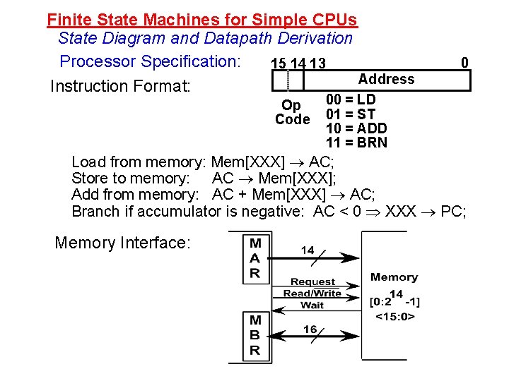
Finite State Machines for Simple CPUs State Diagram and Datapath Derivation Processor Specification: 15 14 13 Address Instruction Format: Op Code 0 00 = LD 01 = ST 10 = ADD 11 = BRN Load from memory: Mem[XXX] AC; Store to memory: AC Mem[XXX]; Add from memory: AC + Mem[XXX] AC; Branch if accumulator is negative: AC < 0 XXX PC; Memory Interface:

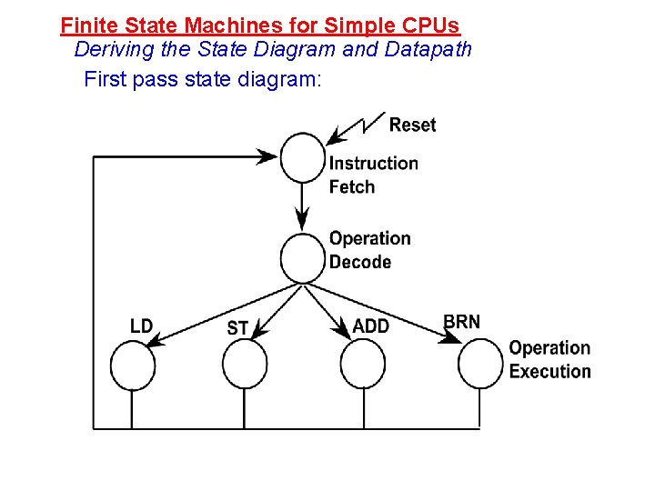
Finite State Machines for Simple CPUs Deriving the State Diagram and Datapath First pass state diagram:

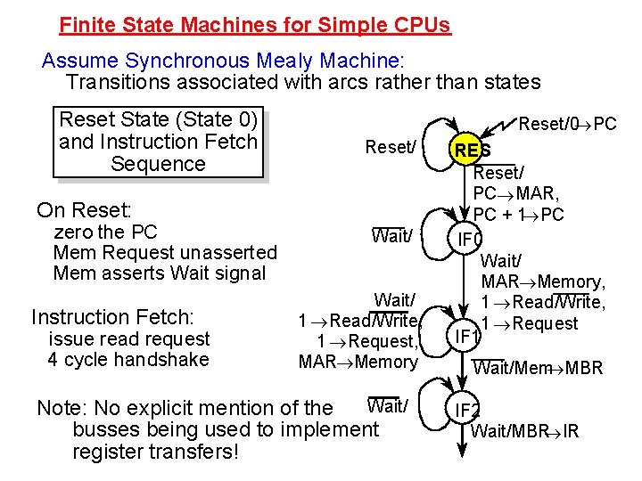
Finite State Machines for Simple CPUs Assume Synchronous Mealy Machine: Transitions associated with arcs rather than states Reset State (State 0) and Instruction Fetch Sequence Reset/0 PC Reset/ On Reset: zero the PC Mem Request unasserted Mem asserts Wait signal Instruction Fetch: issue read request 4 cycle handshake Wait/ 1 Read/Write, 1 Request, MAR Memory Wait/ Note: No explicit mention of the busses being used to implement register transfers! RES Reset/ PC MAR, PC + 1 PC IF 0 Wait/ MAR Memory, 1 Read/Write, 1 Request IF 1 Wait/Mem MBR IF 2 Wait/MBR IR

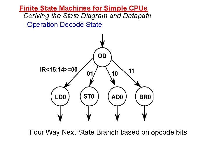
Finite State Machines for Simple CPUs Deriving the State Diagram and Datapath Operation Decode State Four Way Next State Branch based on opcode bits

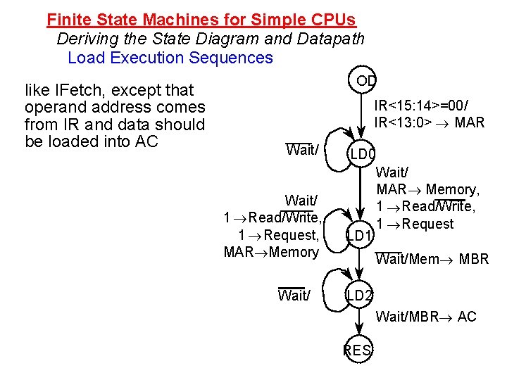
Finite State Machines for Simple CPUs Deriving the State Diagram and Datapath Load Execution Sequences like IFetch, except that operand address comes from IR and data should be loaded into AC OD IR<15: 14>=00/ IR<13: 0> MAR Wait/ 1 Read/Write, 1 Request, MAR Memory Wait/ LD 0 LD 1 Wait/ MAR Memory, 1 Read/Write, 1 Request Wait/Mem MBR LD 2 Wait/MBR AC RES

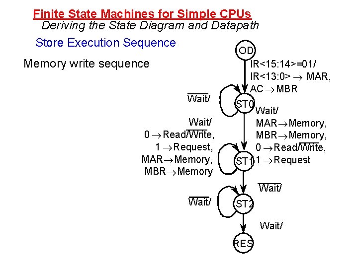
Finite State Machines for Simple CPUs Deriving the State Diagram and Datapath Store Execution Sequence Memory write sequence Wait/ 0 Read/Write, 1 Request, MAR Memory, MBR Memory OD IR<15: 14>=01/ IR<13: 0> MAR, AC MBR ST 0 Wait/ MAR Memory, MBR Memory, 0 Read/Write, ST 1 1 Request Wait/ ST 2 Wait/ RES

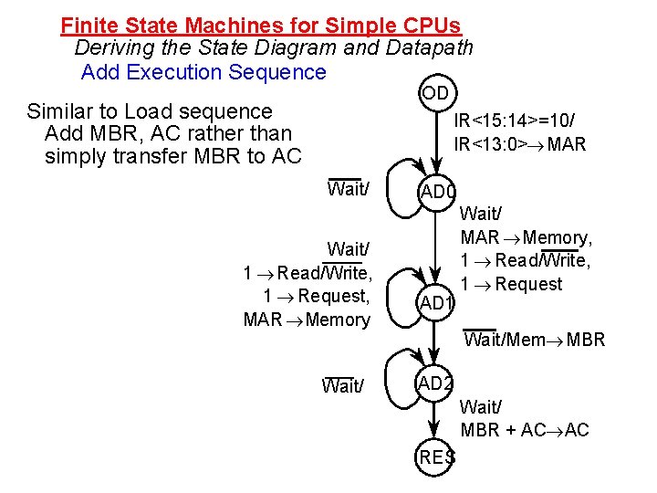
Finite State Machines for Simple CPUs Deriving the State Diagram and Datapath Add Execution Sequence OD Similar to Load sequence Add MBR, AC rather than simply transfer MBR to AC IR<15: 14>=10/ IR<13: 0> MAR Wait/ 1 Read/Write, 1 Request, MAR Memory Wait/ AD 0 AD 1 Wait/ MAR Memory, 1 Read/Write, 1 Request Wait/Mem MBR AD 2 Wait/ MBR + AC AC RES

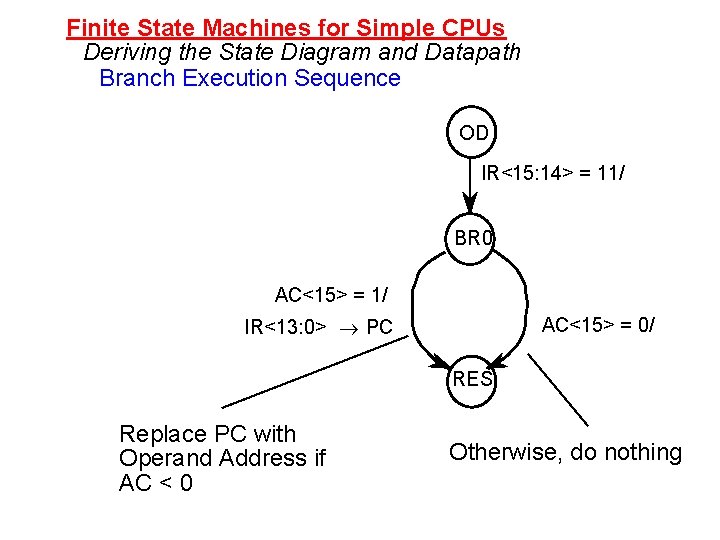
Finite State Machines for Simple CPUs Deriving the State Diagram and Datapath Branch Execution Sequence OD IR<15: 14> = 11/ BR 0 AC<15> = 1/ AC<15> = 0/ IR<13: 0> PC RES Replace PC with Operand Address if AC < 0 Otherwise, do nothing

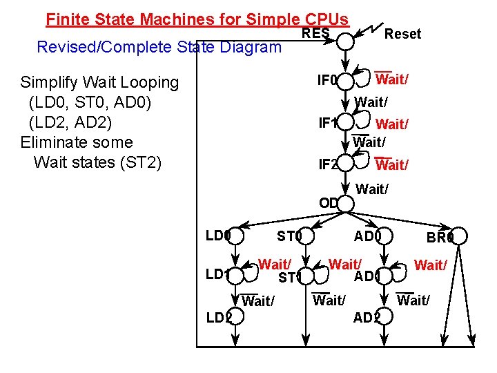
Finite State Machines for Simple CPUs Revised/Complete State Diagram RES IF 0 Simplify Wait Looping (LD 0, ST 0, AD 0) (LD 2, AD 2) Eliminate some Wait states (ST 2) Reset Wait/ IF 1 Wait/ IF 2 Wait/ OD Wait/ LD 0 ST 0 AD 0 LD 1 Wait/ ST 1 Wait/ AD 1 Wait/ LD 2 Wait/ BR 0 Wait/ AD 2

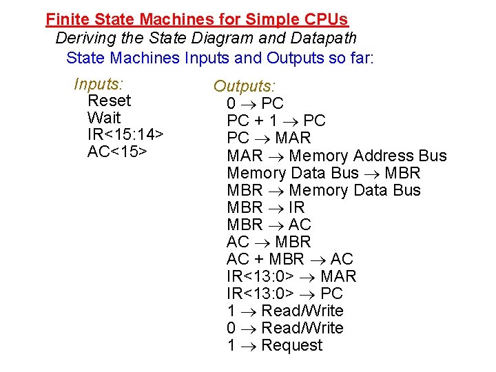
Finite State Machines for Simple CPUs Deriving the State Diagram and Datapath State Machines Inputs and Outputs so far: Inputs: Reset Wait IR<15: 14> AC<15> Outputs: 0 PC PC + 1 PC PC MAR Memory Address Bus Memory Data Bus MBR Memory Data Bus MBR IR MBR AC AC MBR AC + MBR AC IR<13: 0> MAR IR<13: 0> PC 1 Read/Write 0 Read/Write 1 Request

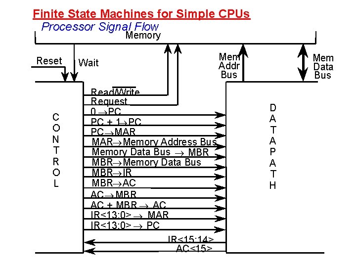
Finite State Machines for Simple CPUs Processor Signal Flow Memory Reset C O N T R O L Wait Read/Write Request 0 PC PC + 1 PC PC MAR Memory Address Bus Memory Data Bus MBR Memory Data Bus MBR IR MBR AC AC MBR AC + MBR AC IR<13: 0> MAR IR<13: 0> PC IR<15: 14> AC<15> Mem Addr Bus Mem Data Bus D A T A P A T H

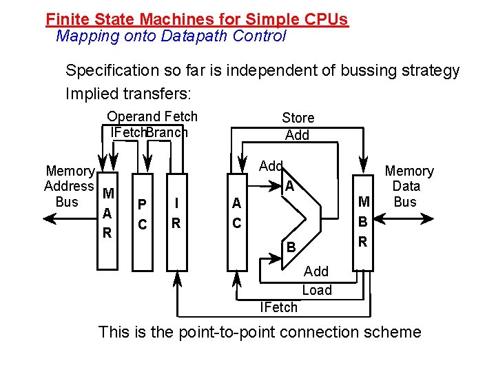
Finite State Machines for Simple CPUs Mapping onto Datapath Control Specification so far is independent of bussing strategy Implied transfers: Operand Fetch IFetch. Branch Memory Address M Bus A R Store Add A P C I R M B R A C B Memory Data Bus Add Load IFetch This is the point-to-point connection scheme

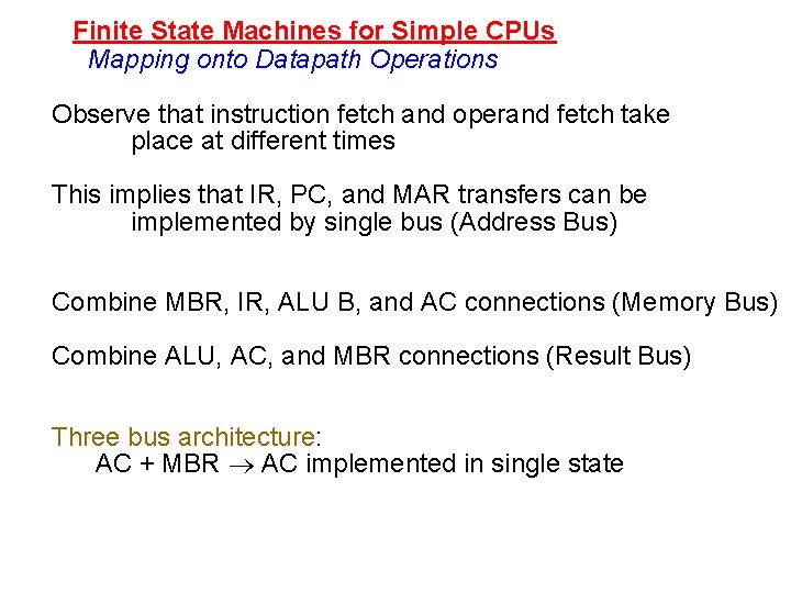
Finite State Machines for Simple CPUs Mapping onto Datapath Operations Observe that instruction fetch and operand fetch take place at different times This implies that IR, PC, and MAR transfers can be implemented by single bus (Address Bus) Combine MBR, IR, ALU B, and AC connections (Memory Bus) Combine ALU, AC, and MBR connections (Result Bus) Three bus architecture: AC + MBR AC implemented in single state

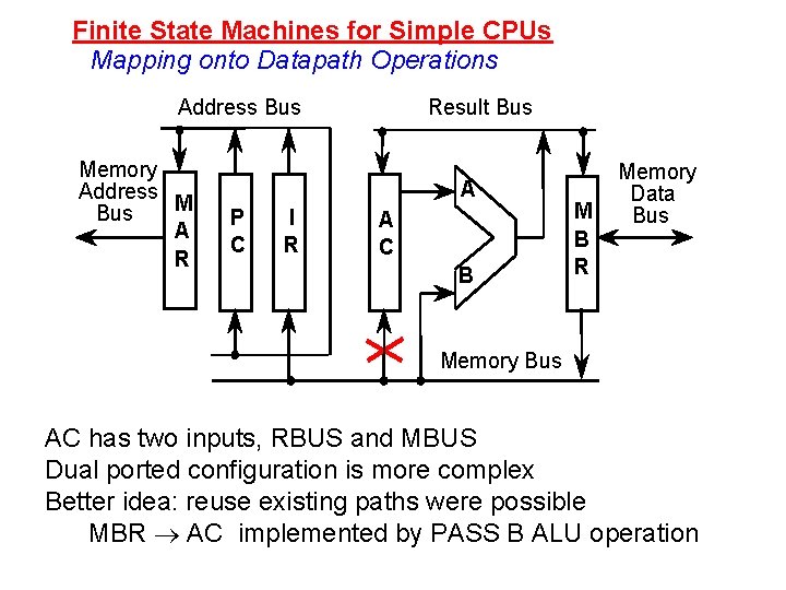
Finite State Machines for Simple CPUs Mapping onto Datapath Operations Address Bus Memory Address M Bus A R Result Bus A P C I R A C B M B R Memory Data Bus Memory Bus AC has two inputs, RBUS and MBUS Dual ported configuration is more complex Better idea: reuse existing paths were possible MBR AC implemented by PASS B ALU operation

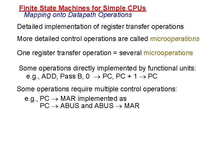
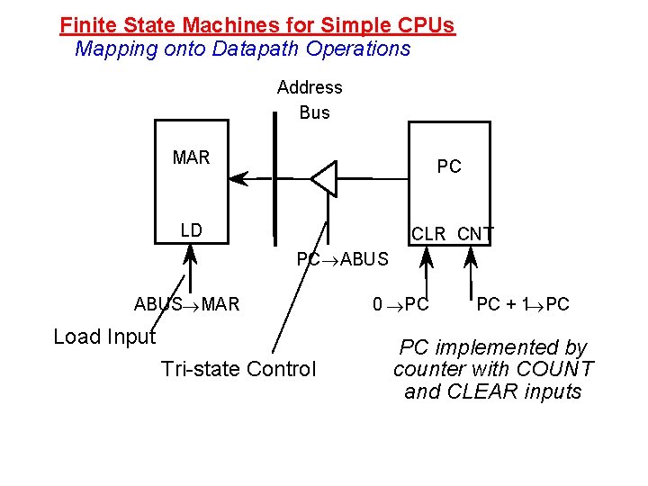
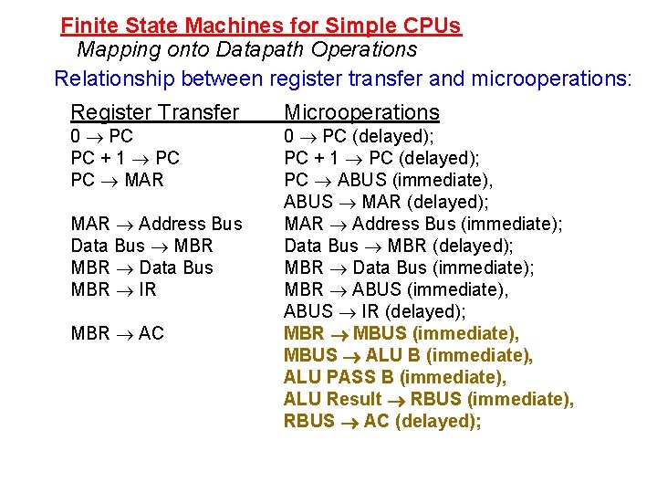
Finite State Machines for Simple CPUs Mapping onto Datapath Operations Detailed implementation of register transfer operations More detailed control operations are called microoperations One register transfer operation = several microoperations Some operations directly implemented by functional units: e. g. , ADD, Pass B, 0 PC, PC + 1 PC Some operations require multiple control operations: e. g. , PC MAR implemented as PC ABUS and ABUS MAR

Finite State Machines for Simple CPUs Mapping onto Datapath Operations Address Bus MAR PC LD CLR CNT PC ABUS MAR Load Input Tri-state Control 0 PC PC + 1 PC PC implemented by counter with COUNT and CLEAR inputs

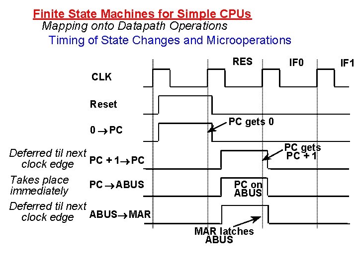
Finite State Machines for Simple CPUs Mapping onto Datapath Operations Timing of State Changes and Microoperations RES IF 0 CLK Reset 0 PC Deferred til next clock edge PC + 1 PC Takes place PC ABUS immediately Deferred til next clock edge ABUS MAR PC gets 0 PC gets PC + 1 PC on ABUS MAR latches ABUS IF 1

Finite State Machines for Simple CPUs Mapping onto Datapath Operations Relationship between register transfer and microoperations: Register Transfer 0 PC PC + 1 PC PC MAR Address Bus Data Bus MBR Data Bus MBR IR MBR AC Microoperations 0 PC (delayed); PC + 1 PC (delayed); PC ABUS (immediate), ABUS MAR (delayed); MAR Address Bus (immediate); Data Bus MBR (delayed); MBR Data Bus (immediate); MBR ABUS (immediate), ABUS IR (delayed); MBR MBUS (immediate), MBUS ALU B (immediate), ALU PASS B (immediate), ALU Result RBUS (immediate), RBUS AC (delayed);

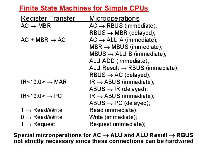
Finite State Machines for Simple CPUs Register Transfer Microoperations AC MBR AC + MBR AC IR<13: 0> MAR IR<13: 0> PC 1 Read/Write 0 Read/Write 1 Request AC RBUS (immediate), RBUS MBR (delayed); AC ALU A (immediate), MBR MBUS (immediate), MBUS ALU B (immediate), ALU ADD (immediate), ALU Result RBUS (immediate), RBUS AC (delayed); IR ABUS (immediate), ABUS IR (delayed); IR ABUS (immediate), ABUS PC (delayed); Read (immediate); Write (immediate); Request (immediate); Special microoperations for AC ALU and ALU Result RBUS not strictly necessary since these connections can be hardwired

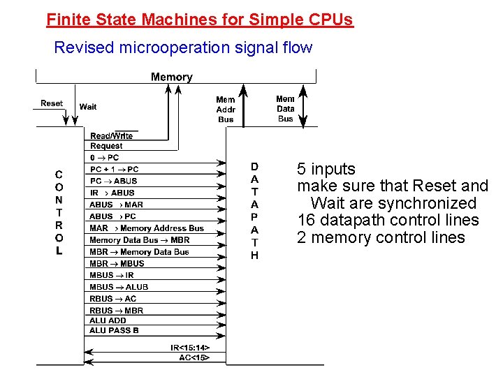
Finite State Machines for Simple CPUs Revised microoperation signal flow 5 inputs make sure that Reset and Wait are synchronized 16 datapath control lines 2 memory control lines