Computer Organization CT 213 Computing Systems Organization Zynq7000


- Slides: 33

Computer Organization CT 213 – Computing Systems Organization

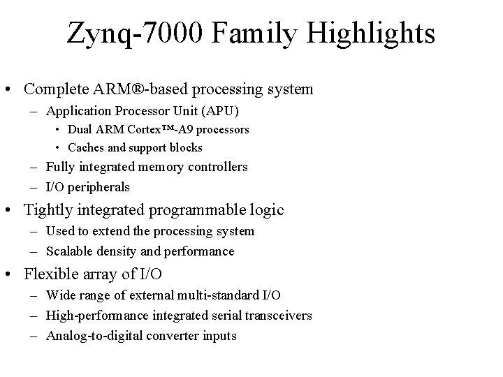
Zynq-7000 Family Highlights • Complete ARM®-based processing system – Application Processor Unit (APU) • Dual ARM Cortex™-A 9 processors • Caches and support blocks – Fully integrated memory controllers – I/O peripherals • Tightly integrated programmable logic – Used to extend the processing system – Scalable density and performance • Flexible array of I/O – Wide range of external multi-standard I/O – High-performance integrated serial transceivers – Analog-to-digital converter inputs

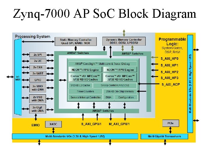
Zynq-7000 AP So. C Block Diagram

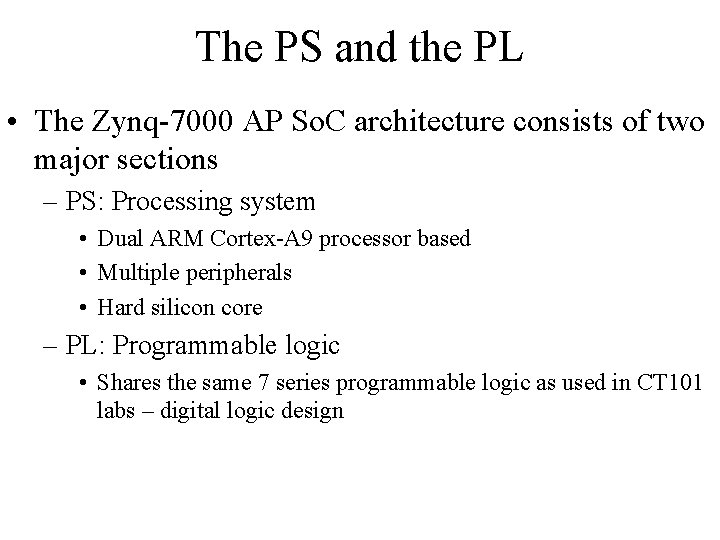
The PS and the PL • The Zynq-7000 AP So. C architecture consists of two major sections – PS: Processing system • Dual ARM Cortex-A 9 processor based • Multiple peripherals • Hard silicon core – PL: Programmable logic • Shares the same 7 series programmable logic as used in CT 101 labs – digital logic design

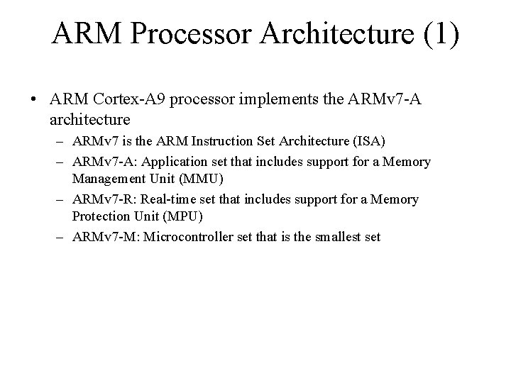
ARM Processor Architecture (1) • ARM Cortex-A 9 processor implements the ARMv 7 -A architecture – ARMv 7 is the ARM Instruction Set Architecture (ISA) – ARMv 7 -A: Application set that includes support for a Memory Management Unit (MMU) – ARMv 7 -R: Real-time set that includes support for a Memory Protection Unit (MPU) – ARMv 7 -M: Microcontroller set that is the smallest set

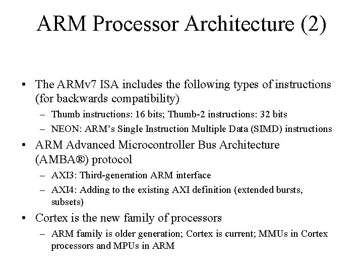
ARM Processor Architecture (2) • The ARMv 7 ISA includes the following types of instructions (for backwards compatibility) – Thumb instructions: 16 bits; Thumb-2 instructions: 32 bits – NEON: ARM’s Single Instruction Multiple Data (SIMD) instructions • ARM Advanced Microcontroller Bus Architecture (AMBA®) protocol – AXI 3: Third-generation ARM interface – AXI 4: Adding to the existing AXI definition (extended bursts, subsets) • Cortex is the new family of processors – ARM family is older generation; Cortex is current; MMUs in Cortex processors and MPUs in ARM

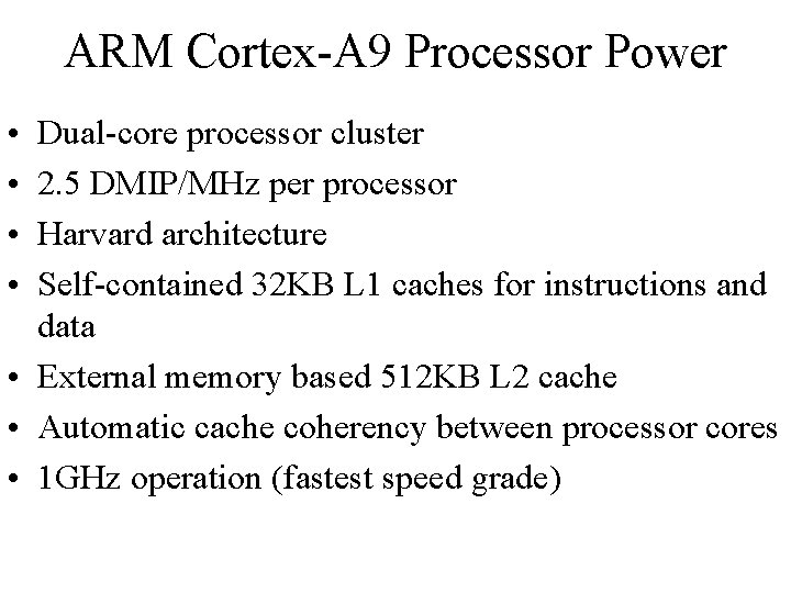
ARM Cortex-A 9 Processor Power • • Dual-core processor cluster 2. 5 DMIP/MHz per processor Harvard architecture Self-contained 32 KB L 1 caches for instructions and data • External memory based 512 KB L 2 cache • Automatic cache coherency between processor cores • 1 GHz operation (fastest speed grade)

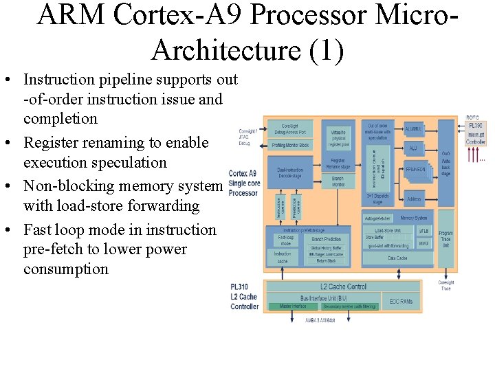
ARM Cortex-A 9 Processor Micro. Architecture (1) • Instruction pipeline supports out -of-order instruction issue and completion • Register renaming to enable execution speculation • Non-blocking memory system with load-store forwarding • Fast loop mode in instruction pre-fetch to lower power consumption

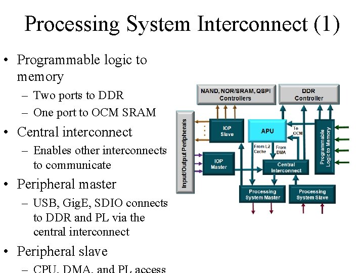
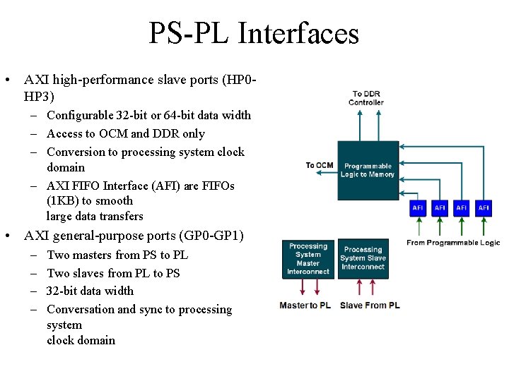
Processing System Interconnect (1) • Programmable logic to memory – Two ports to DDR – One port to OCM SRAM • Central interconnect – Enables other interconnects to communicate • Peripheral master – USB, Gig. E, SDIO connects to DDR and PL via the central interconnect • Peripheral slave

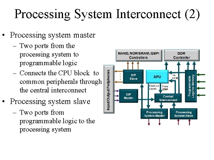
Processing System Interconnect (2) • Processing system master – Two ports from the processing system to programmable logic – Connects the CPU block to common peripherals through the central interconnect • Processing system slave – Two ports from programmable logic to the processing system

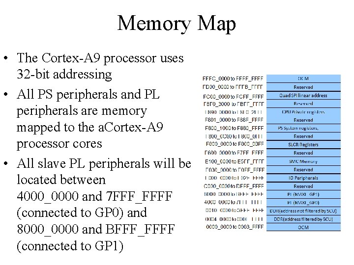
Memory Map • The Cortex-A 9 processor uses 32 -bit addressing • All PS peripherals and PL peripherals are memory mapped to the a. Cortex-A 9 processor cores • All slave PL peripherals will be located between 4000_0000 and 7 FFF_FFFF (connected to GP 0) and 8000_0000 and BFFF_FFFF (connected to GP 1)

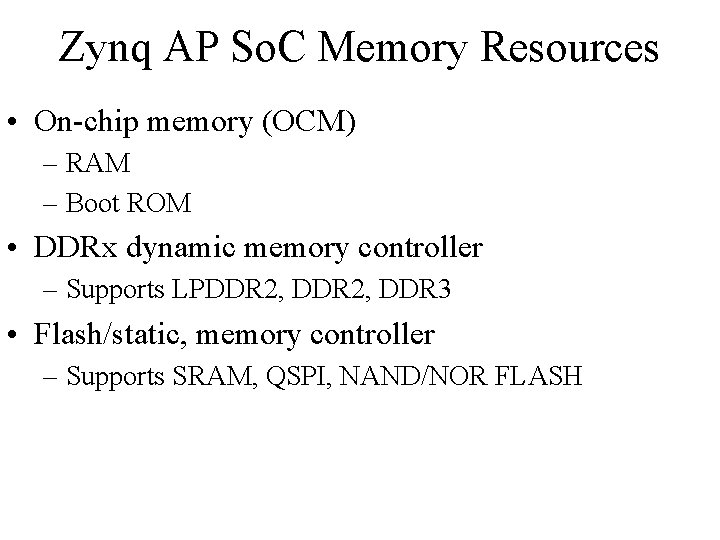
Zynq AP So. C Memory Resources • On-chip memory (OCM) – RAM – Boot ROM • DDRx dynamic memory controller – Supports LPDDR 2, DDR 3 • Flash/static, memory controller – Supports SRAM, QSPI, NAND/NOR FLASH

PS Boots First • CPU 0 boots from OCM ROM; CPU 1 goes into a sleep state • On-chip boot loader in OCM ROM (Stage 0 boot) • Processor loads First Stage Boot Loader (FSBL) from external flash memory – NOR – NAND – Quad-SPI – SD Card – JTAG; not a memory device—used for development/debug only

Configuring the PL • The programmable logic is configured after the PS boots • Performed by application software accessing the hardware device configuration unit – Bitstream image transferred – 100 -MHz, 32 -bit PCAP stream interface – Decryption/authentication hardware option for encrypted bitstreams • In secure boot mode, this option can be used for software memory load – Built-in DMA allows simultaneous PL configuration and

Input/Output Peripherals • • • Two Gig. E Two USB Two SPI Two SD/SDIO Two CAN Two I 2 C Two UART Four 32 -bit GPIOs Static memories – NAND, NOR/SRAM, Quad SPI • Trace ports

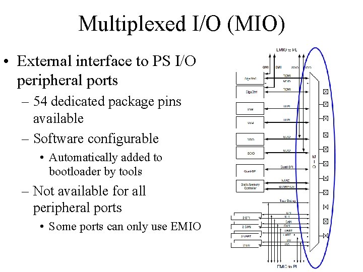
Multiplexed I/O (MIO) • External interface to PS I/O peripheral ports – 54 dedicated package pins available – Software configurable • Automatically added to bootloader by tools – Not available for all peripheral ports • Some ports can only use EMIO

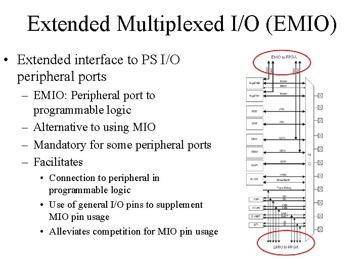
Extended Multiplexed I/O (EMIO) • Extended interface to PS I/O peripheral ports – EMIO: Peripheral port to programmable logic – Alternative to using MIO – Mandatory for some peripheral ports – Facilitates • Connection to peripheral in programmable logic • Use of general I/O pins to supplement MIO pin usage • Alleviates competition for MIO pin usage

PS-PL Interfaces • AXI high-performance slave ports (HP 0 HP 3) – Configurable 32 -bit or 64 -bit data width – Access to OCM and DDR only – Conversion to processing system clock domain – AXI FIFO Interface (AFI) are FIFOs (1 KB) to smooth large data transfers • AXI general-purpose ports (GP 0 -GP 1) – – Two masters from PS to PL Two slaves from PL to PS 32 -bit data width Conversation and sync to processing system clock domain

PS-PL Interfaces • One 64 -bit accelerator coherence port (ACP) AXI slave interface to CPU memory • DMA, interrupts, events signals – Processor event bus for signaling event information to the CPU – PL peripheral IP interrupts to the PS general interrupt controller (GIC) – Four DMA channel RDY/ACK signals • Extended multiplexed I/O (EMIO) allows PS peripheral ports access to PL logic and device I/O pins

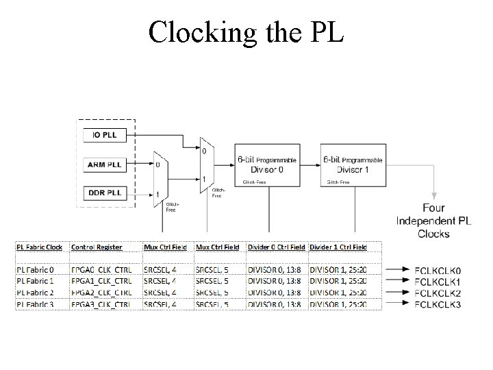
PL Clocking Sources • PS clocks – PS clock source from external package pin – PS has three PLLs for clock generation – PS has four clock ports to PL • The PL has 7 series clocking resources – PL has a different clock source domain compared to the PS – The clock to PL can be sourced from external clock capable pins – Can use one of the four PS clocks as source • Synchronizing the clock between PL and PS is taken care of by the architecture of the PS • PL cannot supply clock source to PS

Clocking the PL

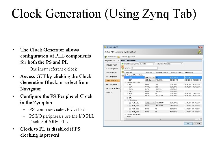
Clock Generation (Using Zynq Tab) • The Clock Generator allows configuration of PLL components for both the PS and PL – One input reference clock • • Access GUI by clicking the Clock Generation Block, or select from Navigator Configure the PS Peripheral Clock in the Zynq tab – PS uses a dedicated PLL clock – PS I/O peripherals use the I/O PLL clock and ARM PLL • Clock to PL is disabled if PS clocking is present

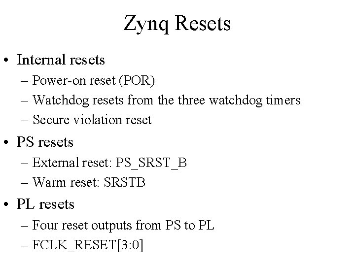
Zynq Resets • Internal resets – Power-on reset (POR) – Watchdog resets from the three watchdog timers – Secure violation reset • PS resets – External reset: PS_SRST_B – Warm reset: SRSTB • PL resets – Four reset outputs from PS to PL – FCLK_RESET[3: 0]

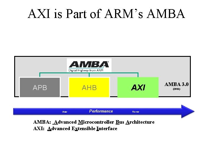
AXI is Part of ARM’s AMBA APB AHB Older Performance AXI Newer AMBA: Advanced Microcontroller Bus Architecture AXI: Advanced Extensible Interface AMBA 3. 0 (2003)

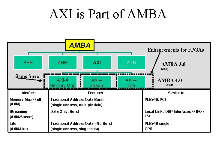
AXI is Part of AMBA APB AHB Enhancements for FPGAs AXI ATB AMBA 3. 0 (2003) Same Spec AXI-4 Memory Map Interface AXI-4 Stream AXI-4 Lite AMBA 4. 0 (2010) Features Similar to Memory Map / Full (AXI 4) Traditional Address/Data Burst PLBv 46, PCI Streaming Data-Only, Burst Local Link / DSP Interfaces / FIFO / FSL Lite Traditional Address/Data—No Burst PLBv 46 -single (AXI 4 -Lite) (single address, single data) OPB (single address, multiple data) (AXI 4 -Stream)

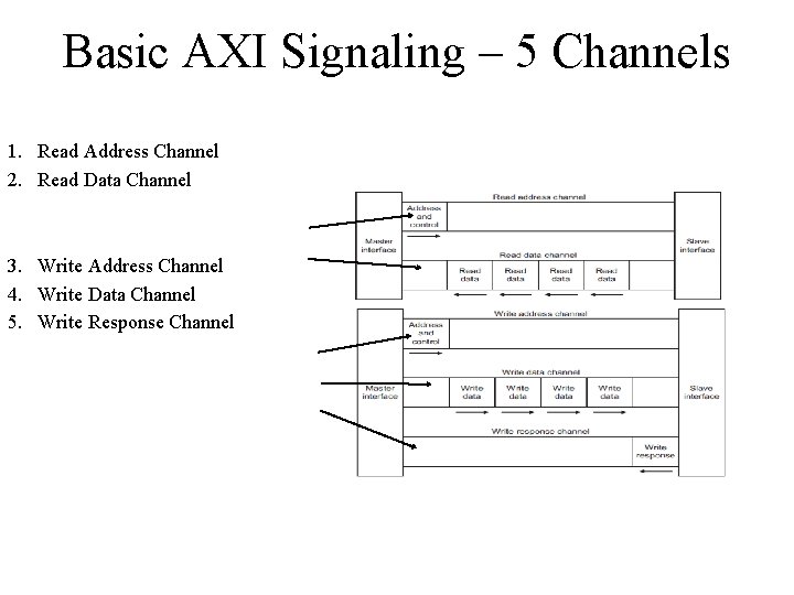
Basic AXI Signaling – 5 Channels 1. Read Address Channel 2. Read Data Channel 3. Write Address Channel 4. Write Data Channel 5. Write Response Channel

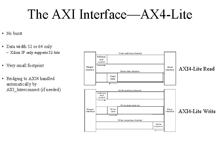
The AXI Interface—AX 4 -Lite • No burst • Data width 32 or 64 only – Xilinx IP only supports 32 -bits • Very small footprint AXI 4 -Lite Read • Bridging to AXI 4 handled automatically by AXI_Interconnect (if needed) AXI 4 -Lite Write

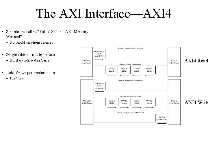
The AXI Interface—AXI 4 • Sometimes called “Full AXI” or “AXI Memory Mapped” – Not ARM-sanctioned names • Single address multiple data – Burst up to 256 data beats AXI 4 Read • Data Width parameterizable – 1024 bits AXI 4 Write

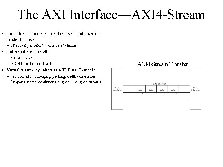
The AXI Interface—AXI 4 -Stream • No address channel, no read and write, always just master to slave – Effectively an AXI 4 “write data” channel • Unlimited burst length – AXI 4 max 256 – AXI 4 -Lite does not burst • Virtually same signaling as AXI Data Channels – Protocol allows merging, packing, width conversion – Supports sparse, continuous, aligned, unaligned streams AXI 4 -Stream Transfer

Streaming Applications • May not have packets –E. g. Digital up converter • No concept of address • Free-running data (in this case) • In this situation, AXI 4 -Stream would optimize to a very simple interface • May have packets – E. g. PCIe • Their packets may contain different information • Typically bridge logic of some sort is needed

Summary • The Zynq-7000 processing platform is a system on a chip (So. C) processor with embedded programmable logic • The processing system (PS) is the hard silicon dual core consisting of – APU and list components • • Two Cortex-A 9 processors NEON co-processor General interrupt controller (GIC) General and watchdog timers – I/O peripherals – External memory interfaces

Summary • The programmable logic (PL) consists of 7 series devices • AXI is an interface providing high performance through point-to-point connection • AXI has separate, independent read and write interfaces implemented with channels • The AXI 4 interface offers improvements over AXI 3 and defines – Full AXI memory mapped – AXI Lite

References • www. Xilinx. com