Computer Organization Architecture CHAPTER ONE 1 Introduction Computer


 A B x = A⊕ B or")

 x+0=x (3) x+1=1 (5) x+x=x (7) x +")


 ØA Boolean function represented by a truth table is plotted into")


 = Σ(0, 2, 4, 5, 6) The simplified expressions")
=Σ(0, 1, 2, 6, 8, 9, 10) fig 1.")

 ØThis approach is similar to the Sum-of-Products simplification, but identifying adjacent")


 Demultiplexers 33")


")


 the memory cells can be accessed for information from any")


- Slides: 64
Computer Organization & Architecture CHAPTER ONE 1
Introduction Computer Organization, Computer Design, Computer Architecture Computer Organization : üis concerned with the way the hardware computer operate and the way they are connected together to form the computer system. üThe various components are assumed to be in place and the task is to investigate the organizational structure to verify that the computer parts operation as intended. Computer Design: v is concerned with the hardware design of the computer. v. Once the computer specification is formulated, it is the task of the designer to develop hardware for the system. v. It is concerned with the determination of what hardware should be used and how the parts should be connected. v. It is the aspect of computer hardware and sometimes referred to as computer implementation. 2
Cont…. Computer Architecture: v is concerned with the structure and behavior of the computer as seen by the user. v. It includes the information formats, the instruction set and techniques for addressing memory. Digital Logic Circuits §This chapter introduces the fundamental knowledge needed for the design of digital systems constructed with the individual gates and flip – flops. § It covers Boolean algebra, combinational circuits and sequential circuits. §This provides the necessary background for understanding the digital circuits to be presented. 3
Digital Computers ØDigital computers use the binary number system, which has two digits, 0 and 1 ØA binary digit is called a bit. ØBits are grouped together as bytes and words to form some type of representation within the computer. ØA sequence of instructions for the computer is known as program. ØBlock diagram of a digital computer as shown fig 1. 1 4
Fig 1. 1 5
The hardware of the computer is usually divided into three major parts. ØThe Central processing Unit (CPU): contains an arithmetic and logic unit for manipulating data, a number of registers for storing data, and control circuits for fetching and executing instructions. ØThe memory of a computer; contains storage for instructions and data, it is called a Random Access Memory (RAM) , the CPU can access any location in memory at random and retrieve the binary information within a fixed interval of time. ØThe input and output processor: contains electronic circuit for communication and controlling the transfer of information between the computer and the outside world. ØThe input and output device: connected to the computer include keyboards, printers, terminals, magnetic disk drives and other communication devices. 6
Logic Gates ØGates are the fundamental building block of all digital logic circuits. ØLogical functions are implemented by the interconnection of gates. ØBinary information is represented in digital computers using electrical signals. ØThese signals can be represented by voltage to specify one of two possible states. For example, if a wire contains a signal of 3 volts, it is considered to contain the digital value 1. ØLikewise, if the wire contains 1. 5 volts, then it represents the digital value 0. ØThe manipulation of binary information in a computer is done using logic circuits called gates. Examples: AND, OR, Inverter, Buffer, NAND, NOR, X-NOR ØEach gate is defined in three ways: graphic symbol, algebraic notation/function, and truth table 7
Fig 1. 2 A. AND Gate A B The truth table of AND gate B. OR Gate A B X=A+B The truth table of OR gate 8
C. Inverter X = A’ D. Buffer X=A E. NAND 9
F. NOR A B G. Exclusive-OR (XOR) A B x = A⊕ B or x=A’B+AB’ H. Exclusive-NOR X = (A⊕ B)’ 10
Boolean Algebra Boolean algebra is an algebra that deals with binary variables and logic operations. Variables are designated by letters such as A, B, x, and y. A Boolean function can be expressed algebraically with binary variables, the logic operation symbols, parentheses, and equal sign, and it can represent by: truth table, logic diagram & algebraic expression The result of a Boolean function is either 0 or 1. Example: Consider the following Boolean function: F = xy + z‘ The function F is equal to 1 if either both x and y are 1 or z' is 1; F is equal to 0 otherwise. NB: z' = 1 is equivalent to saying z = 0 since z' is the complement of z. 11
Basic Identities of Boolean algebra (1) x+0=x (3) x+1=1 (5) x+x=x (7) x + x' = 1 (9) x+y=y+x (11) x + (y + z) = (x + y) + z (13) x(y + z) = xy + xz (15) (x + y)' = x'y' (17) (x')' = x (2) (4) (6) (8) (10) (12) (14) (16) x*0=0 x*1=x x*x=x x * x' = 0 xy = yx x(yz) = (xy)z x + yz = (x + y)(x + z) (xy)' = x' + y‘ De-Morgan’s Theorem This theorem is very important in dealing with NOR and NAND gates. It states that a NOR gate that performs the (x+y)’ function is equivalent to the function x’y’. Similarly a NAND function can be expressed by either (xy)’ or (x’+y’). For this reason the NOR and NAND gates have two distinct graphic symbols. 12
OR invert AND v. The invert AND symbol for the NOR gate follows from the De-Morgan’s thermo and from the convention that small circles denote complementation. v. Similarly the NAND gates have two distinct symbols as shown below. Invert OR x Y z AND-invert x y z 13
Complement of a function ØThe complement of a function F when expressed in a truth table is obtained by interchanging 1’s and 0’s in the values of F in the truth table. ØWhen the function is expressed in algebraic form the complement of the function can be derived by means of De-Morgan’s Theorem. The general form of De. Morgan’s theorem can be expressed as follows: (x 1+x 2+x 3+…. Xn) = x 1’x 2’x 3’…xn’ (x 1 x 2 x 3…xn)’ =x 1’+x 2’+x 3’+…+xn’ ØBy changing all OR operation to AND operation and all OR operations and then complementing each individual letter variable we can derive a simple procedure for obtaining the complement of an algebraic expression. Eg. F = AB+C’D’+B’D F’=(A’+B’)(C+D)(B+D’) NB: The complement expression is obtained by interchanging AND and OR operations and complementing each individual. 14
Map Simplification In addition to using Boolean algebra to simplify a Boolean function, we use map simplification techniques/methods. The map method is known as the Karnaugh map or K-map. Each combination of the variables in a truth table is called a minterm. There are 2 n minterms for a function of n variables. The Boolean algebra can simplify by those two methods: 1. Sum-of- Products simplifications (SOP) 2. Product-of-sum simplifications (POS) 15
Variable Maps The following are maps for two-, three-, and four-variable function: fig 1. 3 16
Cont……. ØThe variable names are listed across both the sides of the diagonal line into the corner of the map. ØThe 0’s and the 1’s marked along each row and each column designate the value of the variables. ØEach variable under the brackets contain half of the squares in the map where that variable appears unprimed. ØThe minterm represent by a square is determined from the binary assignment of the variable along the left top edges in the map. ØHere the min term 5 the three variable maps are 101 of the second column. This minterm represents a value for the binary variables A, B and C with A and C being unprimed and B being primed. 17
Sum-of-Products Simplification ((SOP) ØA Boolean function represented by a truth table is plotted into the map by inserting 1's into those squares where the function is 1. ØBoolean functions can then be simplified by identifying adjacent squares in the Karnaugh map that contain a 1. ØA square is considered adjacent to another square if it is next to, above, or below it. In addition, squares at the extreme ends of the same horizontal row are also considered adjacent. The same applies to the top and bottom squares of a column. ØThe objective to identify adjacent squares containing 1's and group them together. ØGroups must contain a number of squares that is an integral power of 2. 18
Groups of combined adjacent squares may share one or more squares with one or more groups. Each group of squares represents an algebraic term, and the OR of those terms gives the simplified algebraic expression for the function. To find the most simplified algebraic expression, the goal of map simplification is to identify the least number of groups with the largest number of members. Example: We will simplify the Boolean function. F (A, B, C) = Σ(3, 4, 6, 7) There are four squares marked with 1’s, one for each minterm that produces 1 for the function. These squares belong to minterm 3, 4, 6, 7 and are recognized from the figure b. Two adjacent squares are combined in the third column. This column belongs to both B and C produces the term BC. The remaining two squares with 1’s in the two corner of the second row are adjacent and belong to row columns of C’, so they produce the term AC’. 19
§The simplified expression for the function is the or of the two terms: F = BC + AC’ §The second example simplifies the following Boolean function: F(A, B, C) = Σ(0, 2, 4, 5, 6) §The five minterms are marked with 1’s in the corresponding squares of the three variable maps. §The four squares in the first and the fourth columns are adjacent and represent the term C’. §The remaining square marked with a 1 belongs to minterm 5 and can be combined with the square of minterm 4 to produce the term AB’. The simplified function is 20
Map for F(A, B, C) = Σ(0, 2, 4, 5, 6) The simplified expressions of the function is : F = C’+AB’ 21
Maps for F(A, B, C, D)=Σ(0, 1, 2, 6, 8, 9, 10) fig 1. 4 22
ØThe area in the map covered by this four variable consists of the squares marked with 1’s in fig 1. 4. ØThe function contains 1’s in the four corners that when taken as groups give the term B’D’. This is possible because these four squares are adjacent when the map is considered with the top and bottom or left and right edges touching. ØThe two 1’s on the bottom row are combined with the two 1’s on the left of the bottom row to give the term B’C’. ØThe remaining 1 in the square of minterm 6 is combined with the minterm 2 to give the term A’CD’. So the simplified function is: F = B’D’ + B’C’ + A’CD’ 23
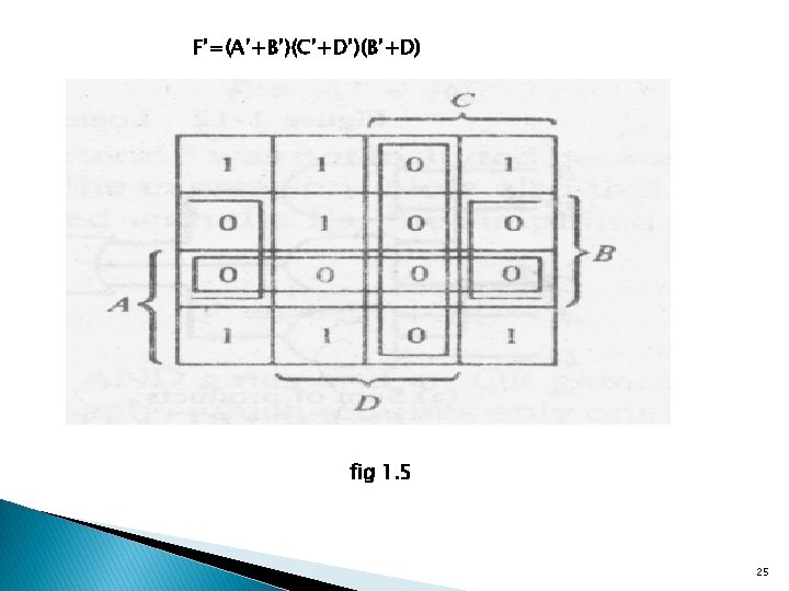
Product-of-Sums Simplification (POS) ØThis approach is similar to the Sum-of-Products simplification, but identifying adjacent squares containing 0’s instead of 1’s forms the groups of adjacent squares. ØThen, instead of representing the function as a sum of products, the function is represented as a product of sums. Examples: F(A, B, C, D) = Σ(0, 1, 2, 5, 8, 9, 10) ØThe 1’s marked in the map of fig 1. 5 represents the minterms that produces a 1 for the function, ØThe squares marked with 0’s represent the minterm not included in F and therefore denote the complement of F. ØCombining the squares with 1’s gives the simplified function in sum-of-products form: F = B’D’ +B’C’+A’C’D ØIf the squares marked with 0’s are combined as shown in the diagram, we obtain the simplified complement function: 24
Fig 1. 6 26
Fig 1. 7 27
Don't Care Conditions It doesn't matter whether a function produces a 0 or 1 for a given minterm. When this condition occurs, an X is used in the map to represent the don't care condition. Then, when performing map simplification, a square containing an X can be used in both the Sum-of-Products approach and the Product-of-Sums approach. When choosing adjacent squares for the function in the map, the x’s may be assumed to be either 0 or 1, whichever gives the simplest expression In addition an x need not to be used at all if it does not contribute to the simplification of the function. In each case the choice depends only on the simplification that can be achieved. As example consider the following Boolean function together with the don’t care minterms: F(A, B, C) = Σ 0, 2, 6) d(A, B, C) = Σ(1, 3, 5) 28
The minterm listed with F produce a 1 for the function. The don’t care minterms listed with d may produce either a 0 or 1 for the function. The remaining minterms 4, 7 produce a 0 for the function. The 1’s and x’s are combined in any convenient manner so as to enclose the maximum number of adjacent squares. It is not necessary to include the don’t care minterms 1 and 3 with the 1’s in the first row we obtain the term, BC’. The simplified expression is: F = A’ + BC’ But if we don’t use the X’s the simplified expression would be: F=A’C’+BC’ it needs two ANDs gate and one OR gates. 29
Combinational Circuits §A combinational circuit is a connected arrangement of logic gates with a set of inputs and outputs. §At any given time, the binary values of the outputs are a function of the binary values of the inputs. §The design of a combinational circuit starts from a verbal outline of the problem and ends in a logic circuit diagram. § The procedure involves the following steps: o. The problem is stated. o. The input and output variables are assigned letter symbols. o. The truth table that defines the relationship between inputs and outputs is derived. o. The logic diagram is drawn 30
Half-Adder The most basic digital arithmetic circuit. Performs the addition of two binary digits. The input variables of a half-adder are called the augends and the addend. The output variables of a half-adder are called the sum and the carry. fig 1. 8 half adder S = x’y+xy’=x ⊕ y C=xy 31
Full-Adder üA full-adder performs the addition of three binary digits. üTwo half-adders can be combined to for a full-adder. üFull adder has three inputs and two outputs üThe full adder circuit contains two half adders and an OR gate. fig 1. 9 Full-adder 32
NB: Additional examples of combinational circuits: Decoders Encoders multiplexers(MUL) Demultiplexers 33
Decoders v. A binary code of n bits is capable of representing up to 2 n distinct elements of the coded information v A decoder is a combinational circuit that converts binary information from the n coded inputs to a maximum of 2 n unique outputs v A decoder has n inputs and m outputs, where m ≤ 2 n, and are called n-to-mline decoders v Each output represents one of the combinations of the input variables v An enable input controls operation of the decoder 34
Fig 1. 20 3 -to- 8 line Decoder 35
Truth table for 3 -to- 8 line Decoder ØSome decoders use NAND gates rather than AND gates causing the outputs to be in their complemented form Ø The circuit would then be enabled when E = 0 36
Fig 1. 21 2 -to-4 line decoder with NAND gates NB: q. It is possible to combine two or more decoders with enable inputs to form a larger decoder q. The enable inputs are a convenient feature for decoder expansion 37
Fig 1. 22 A 3 X 8 Decoder constructed with 2 X 4 Decoders You can check the relationship by using the truth tables. 38
Encoders üAn encoder is a digital circuit that performs the inverse of a decoder ü An encoder has 2 n (or less) input lines and n output lines üThe output lines generate the binary code corresponding to the input value Truth tables for Octal to Binary Encoder 39
Cont… v. An encoder can be implemented with OR gates A 0 = D 1 + D 3 + D 5 + D 7 A 1 = D 2 + D 3 + D 6 + D 7 A 2 = D 4 + D 5 + D 6 + D 7 Multiplexers v. A multiplexer (MUX) is a combinational circuit with 2 n input data lines, n input select lines, and one output line v. The input selection lines determine which input data line is selected for the output 40
Fig 1. 23 4 -to-1 line Multiplexers 41
Cont… üRather than using a truth table to describe the circuit, we use function table with 2 n rows is used , example for the 4 -to-1 line multiplexer above we needs 64 rows, if we use truth table , then instead we use function tables. ü One row for each combination of the selection inputs ü The MUX is also called a data selector Function table for 4 -to- 1 line Multiplexers You can check from fig 1. 23 42
Sequential circuits üthe current output of a sequential circuit depends on the current input and the current state of that circuit. Flip Flops Is the simplest form of sequential circuit There a variety of flip flops, all of which share two properties: 1. The flip-flop is a bistable device. It exists in one of two stable states 2. The flip-flop has two outputs, which are always the complements of each other. These are generally labeled Q and Q’ (Q complement). A Flip-flop is a binary cell capable of storing one bit of information. It has two outputs, one for the normal value and one for the complement value of the bit stored in it. Flip-flops are storage elements utilized in synchronous sequential circuits. 43
Cont…. . Synchronous sequential circuits employ signals that effect storage elements only at discrete instances of time. A timing device called a clock pulse generator that produces a periodic train of clock pulses achieves synchronization. Values maintained in the storage elements can only change when the clock pulses. Hence, a flip-flop maintains a binary state until directed by a clock pulse to switch states. The difference in the types of flip flops is in the number of inputs and the manner in which the inputs affect the binary state. Flip-flops can be described by a characteristic table which permutated all possible inputs (just like a truth table). The characteristic table of a flip-flop describes all possible outputs (called the next state) at time Q(t+1) over all possible inputs and the present state at time Q(t). 44
The most common types of flip flops are: Ø SR Flip-Flop Ø D Flip-Flop Ø JK Flip-Flop Ø T Flip-Flop SR Flip-Flop or S-R Latch Has 3 Inputs: Graphic symbol Truth table §S (for set) §R (for reset) §C(for Clock) Has 2 Outputs: §Q §Q' 45
Cont…. . ØThe operation of the SR flip-flop is as follow. ØIf there is no signal at the clock input C, the output of the circuit cannot change irrespective of the values at inputs S and R. ØOnly when the clock signals changes from 0 to 1 can the output be affected according to the values in inputs S and R ØIf S =1 and R = 0 when C changes from 0 to 1 output Q is set to 1. Ø If S = 0 and R =1 when C changes from 0 to 1 output Q is cleared to 0. ØIf both S and R are 0 during the clock transition, output does not change. ØWhen both S and R are equal to 1, the output is unpredictable and may go to either 0 or 1, depending on internal timing that occur within the circuit 46
D Flip-Flop: = slight modifications of SR flipflops Inputs: Graphics Symbol D (for data) C (for clock) Outputs: Q Q' JK Flip-Flop : is the refinements of the SR flip-flops in that indeterminate conditions of the SR type and is defined in the JK types. -if inputs J& K are both equal to 1 a clock transition switches the outputs of the flip-flops to their complement state. Inputs: J K C Outputs: Q &Q' Graphics Symbol 47
T Flip-Flop : is obtained from a JK types when inputs J& K are connected to provide single inputs designed by T. Ø the T flip flops has only two conditions I. When T=0(J=K=0) a clock transition does not change the state of the flip -flops II. When T=1(J=K=1) a clock transition complements the state of the flipflops Inputs: T (for toggle) C (for clock) Outputs: Q &Q‘ The T flip flops can be expressed by this equation: Q(t+1)=Q(t) XOR T Edge – Triggered Flip-flops Most common types of flip flops used synchronize the state change during a clock transition is the edge-triggered flip- flops. 48
Cont…. ØMost flip-flops are edge-triggered flip-flops (i. e. the transition occurs at a specific level of the clock pulse). ØA positive-edge transition occurs on the rising edge of the clock signal. ØA negative-edge transition occurs on the falling edge of the clock signal. Master Slave flip-flops ØConsists of two flip-flop üThe 1 st is the Master, w/h responds to the positive level of the clock and üThe 2 nd is the Slave, w/h responds to the negative level of the clock. Eg. The result changes from 0 t 0 1 transitions of the clock signals. ØFlip-flops can also include special input terminals for setting or clearing the flipflop asynchronously. ØThese inputs are usually called preset and clear and are useful for initialing the flip-flops before clocked operations are initiated 49
Registers A register is a group of flip-flops with each flip-flop capable of storing one bit of information An n-bit register has a group of n flip-flops A register may also have combinational gates that perform certain dataprocessing tasks The flip-flops hold the data and the gates control when and how new data is transferred into the register The flip-flops have a common clock input A common clear input is available to reset all the flip-flops asynchronously 50
Fig 1. 24 4 bit Registers 51
The transfer of new data into a register is called loading the register If all bits are loaded simultaneously with a common clock pulse transition, then the loading is done in parallel The load input determines the action to be taken with each clock pulse If the load input is 1, then the data in the four inputs are transferred at the next positive clock transition If the load input is 0, the data inputs are inhibited and the output is fed back to simulate a no change condition Two basic types of registers are commonly used: 1. parallel registers and 2. shift registers. 52
NB: Figure 1. 25 illustrates the operation of a parallel register using D flip-flops. Fig 1. 25 8 bit parallel register 53
2. SHIFT REGISTER: A shift register accepts and/or transfers information serially. A shift register is capable of shifting its binary information in one or both directions The logical configuration is a chain of flip-flops, with the output of one connected to the input of the next The serial input determines what goes into the leftmost position during the shift The serial output is taken from the output of the rightmost flip-flop Fig 1. 26 5 bit shift register 54
A bi-directional shift register can shift in both directions The most general shift register has all the following capabilities: ü An input for clock pulses to synchronize all operations ü A shift-right operation and a serial input line associated with the shiftright ü A shift-left operation and a serial input line associated with the shift-left ü A parallel load operation and n input lines associated with the parallel transfer ü n parallel output lines 55
Binary Counters ØA register that goes through a predetermined sequence of states upon the application of input pulses is called a counter Ø The input pulses may be a clock or an external input Ø The input may occur at uniform intervals of time or randomly Ø Used to count the number of occurrences of an event and for generating timing signals to control the sequence of operations Ø A counter that follows the binary number sequence is a binary counter Ø An n-bit binary counter is a register of n flip-flops and gates that follow a sequence of states Ø Consider the sequence 0000, 0001, 0010, 0011, 1000, … Ø The lsb is complemented each count Ø Every other bit is complemented iff all its lower-order bits are equal to 1 56
ØNatural to use either T or JK flip-flops since they both have a complement state Ø The counter has an enable input Ø Synchronous counters have a regular pattern with a common clock Ø The chain of AND gates generate the logic for the flip-flop inputs 57
Fig 1. 27 4 bit synchronous binary counter 58
Memory Unit A memory unit is a collection of storage cells together with associated circuits to transfer information in and out of storage • The memory stores binary data in groups of bits called words • A word can represent an instruction code or alphanumeric characters • Each word in memory is assigned an address from 0 to 2 k – 1, where k is the number of address lines • A decoder inside the memory accepts an address opens the paths needed to select the bits of the specified word • The memory capacity is stated as the total number of bytes that can be stored • Refer to the number of bytes using one of the following o K (kilo) = 210 o G (giga) = 230 o M (mega) = 220 • 64 K = 210, 2 M = 221, and 4 G = 232 • 59
In random-access memory (RAM) the memory cells can be accessed for information from any desired random location • The process of locating a word in memory is the same and requires an equal amount of time no matter where the cells are located physically in memory Communication between memory and its environment is achieved via data input and output lines, address selections lines, and control lines • The n data input lines provide the information to be stored in memory • The n data output lines supply the information coming out of memory • The k address lines provide a binary number of k bits that specify a specific word or location • The two control lines specify the direction of transfer – either read or write 60
Steps to write to memory: ü Apply the binary address of the desired word into the address lines ü Apply the data bits that are to be stored in memory on the data lines ü Activate the write input 61
Steps to read from memory: ü Apply the binary address of the desired word into the address lines ü Activate the read input • A read-only memory (ROM) is a memory unit that performs the read operation only – there is no write capability • The binary information stored in a ROM is permanent during the hardware production • RAM is a general-purpose device whose contents can be altered • The information in ROM forms the required interconnection pattern • ROMs come with special internal electronic fuses that can be programmed for a specific configuration • An m x n ROM is an array of binary cells organized into m words of n bits each 62
v A ROM has k address lines to select one of m words in memory and n output lines, one for each bit of the word v May have one or more enable inputs for expansion v The outputs are a function of only the present input (the address), so it is a combinational circuit constructed of decoders and OR gates 63
ØWhen used as a memory unit, it stores fixed programs that are not to be altered and for tables of constants that will not change Ø When used in the design of control units for digital computers, it stores coded information that represents the sequence of internal control variables to enable the various operations Ø A control unit that utilizes a ROM is called a microprogrammed control unit Ø The required paths may be programmed in three different ways Ø Mask programming is done by the semiconductor company based upon a truth table provided by the manufacturer Ø Programmable read-only memory (PROM) is more economical. PROM units contain all fuses intact and are blown by users Ø Erasable PROM (EPROM) can be altered using a special ultraviolet light Ø Electrical erasable PROM (EEPROM) can be erased with electrical signals 64