COMPUTER ORGANIZATION AND DESIGN The HardwareSoftware Interface Chapter

- Slides: 34

COMPUTER ORGANIZATION AND DESIGN The Hardware/Software Interface Chapter 5 Large and Fast: Exploiting Memory Hierarchy

n n Programs access a small proportion of their address space at any time Temporal locality n n n § 5. 1 Introduction Principle of Locality Items accessed recently are likely to be accessed again soon e. g. , instructions in a loop, induction variables Spatial locality n n Items near those accessed recently are likely to be accessed soon E. g. , sequential instruction access, array data Chapter 5 — Large and Fast: Exploiting Memory Hierarchy — 2

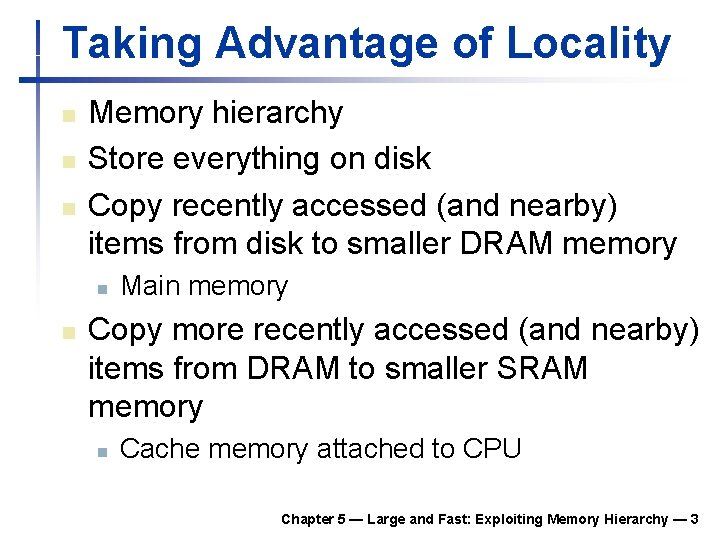
Taking Advantage of Locality n n n Memory hierarchy Store everything on disk Copy recently accessed (and nearby) items from disk to smaller DRAM memory n n Main memory Copy more recently accessed (and nearby) items from DRAM to smaller SRAM memory n Cache memory attached to CPU Chapter 5 — Large and Fast: Exploiting Memory Hierarchy — 3

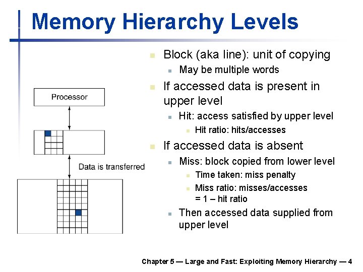
Memory Hierarchy Levels n Block (aka line): unit of copying n n May be multiple words If accessed data is present in upper level n Hit: access satisfied by upper level n n Hit ratio: hits/accesses If accessed data is absent n Miss: block copied from lower level n n n Time taken: miss penalty Miss ratio: misses/accesses = 1 – hit ratio Then accessed data supplied from upper level Chapter 5 — Large and Fast: Exploiting Memory Hierarchy — 4

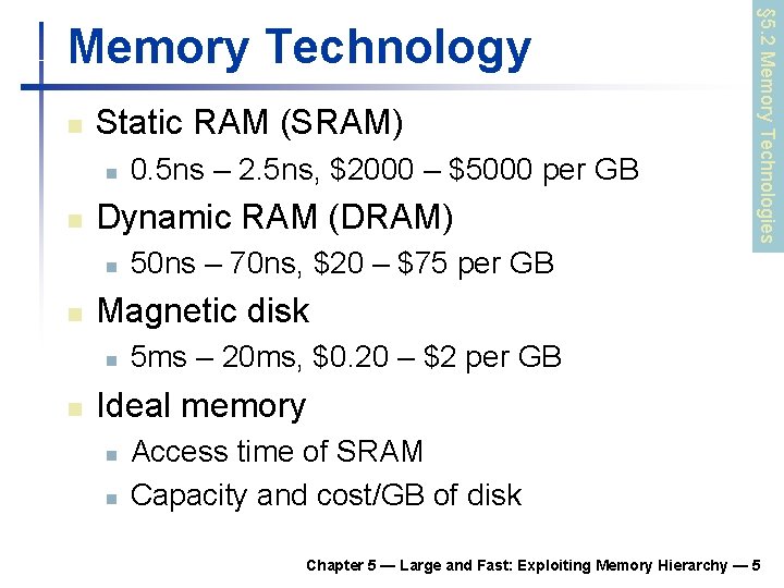
n Static RAM (SRAM) n n Dynamic RAM (DRAM) n n 50 ns – 70 ns, $20 – $75 per GB Magnetic disk n n 0. 5 ns – 2. 5 ns, $2000 – $5000 per GB § 5. 2 Memory Technologies Memory Technology 5 ms – 20 ms, $0. 20 – $2 per GB Ideal memory n n Access time of SRAM Capacity and cost/GB of disk Chapter 5 — Large and Fast: Exploiting Memory Hierarchy — 5

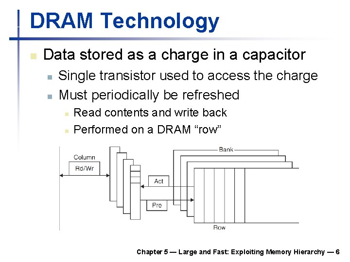
DRAM Technology n Data stored as a charge in a capacitor n n Single transistor used to access the charge Must periodically be refreshed n n Read contents and write back Performed on a DRAM “row” Chapter 5 — Large and Fast: Exploiting Memory Hierarchy — 6

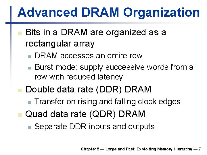
Advanced DRAM Organization n Bits in a DRAM are organized as a rectangular array n n n Double data rate (DDR) DRAM n n DRAM accesses an entire row Burst mode: supply successive words from a row with reduced latency Transfer on rising and falling clock edges Quad data rate (QDR) DRAM n Separate DDR inputs and outputs Chapter 5 — Large and Fast: Exploiting Memory Hierarchy — 7

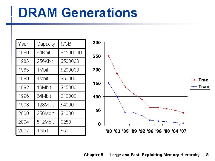
DRAM Generations Year Capacity $/GB 1980 64 Kbit $1500000 1983 256 Kbit $500000 1985 1 Mbit $200000 1989 4 Mbit $50000 1992 16 Mbit $15000 1996 64 Mbit $10000 1998 128 Mbit $4000 256 Mbit $1000 2004 512 Mbit $250 2007 1 Gbit $50 Chapter 5 — Large and Fast: Exploiting Memory Hierarchy — 8

DRAM Performance Factors n Row buffer n n Synchronous DRAM n n n Allows several words to be read and refreshed in parallel Allows for consecutive accesses in bursts without needing to send each address Improves bandwidth DRAM banking n n Allows simultaneous access to multiple DRAMs Improves bandwidth Chapter 5 — Large and Fast: Exploiting Memory Hierarchy — 9

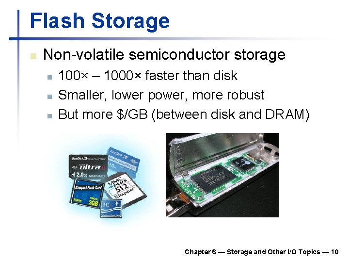
Flash Storage n Non-volatile semiconductor storage n n n 100× – 1000× faster than disk Smaller, lower power, more robust But more $/GB (between disk and DRAM) Chapter 6 — Storage and Other I/O Topics — 10

Flash Types n NOR flash: bit cell like a NOR gate n n n NAND flash: bit cell like a NAND gate n n Random read/write access Used for instruction memory in embedded systems Denser (bits/area), but block-at-a-time access Cheaper GB Used for USB keys, media storage, … Flash bits wears out after 1000’s of accesses n n Not suitable for direct RAM or disk replacement Wear levelling: remap data to less used blocks Chapter 6 — Storage and Other I/O Topics — 11

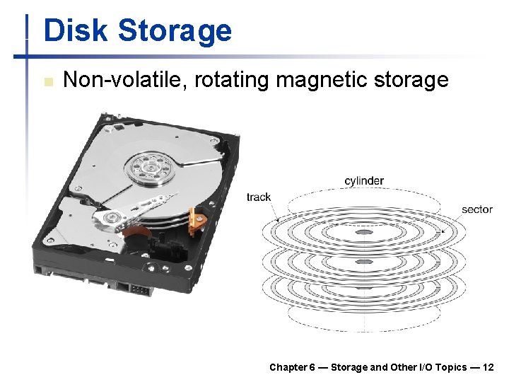
Disk Storage n Non-volatile, rotating magnetic storage Chapter 6 — Storage and Other I/O Topics — 12

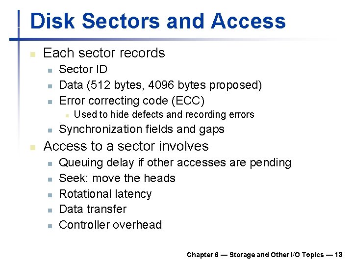
Disk Sectors and Access n Each sector records n n n Sector ID Data (512 bytes, 4096 bytes proposed) Error correcting code (ECC) n n n Used to hide defects and recording errors Synchronization fields and gaps Access to a sector involves n n n Queuing delay if other accesses are pending Seek: move the heads Rotational latency Data transfer Controller overhead Chapter 6 — Storage and Other I/O Topics — 13

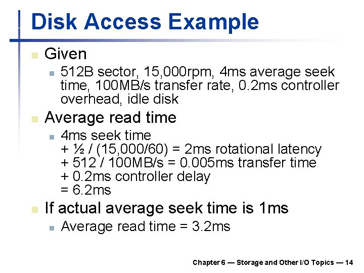
Disk Access Example n Given n n Average read time n n 512 B sector, 15, 000 rpm, 4 ms average seek time, 100 MB/s transfer rate, 0. 2 ms controller overhead, idle disk 4 ms seek time + ½ / (15, 000/60) = 2 ms rotational latency + 512 / 100 MB/s = 0. 005 ms transfer time + 0. 2 ms controller delay = 6. 2 ms If actual average seek time is 1 ms n Average read time = 3. 2 ms Chapter 6 — Storage and Other I/O Topics — 14

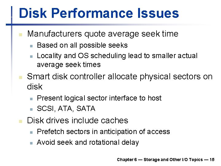
Disk Performance Issues n Manufacturers quote average seek time n n n Smart disk controller allocate physical sectors on disk n n n Based on all possible seeks Locality and OS scheduling lead to smaller actual average seek times Present logical sector interface to host SCSI, ATA, SATA Disk drives include caches n n Prefetch sectors in anticipation of access Avoid seek and rotational delay Chapter 6 — Storage and Other I/O Topics — 15

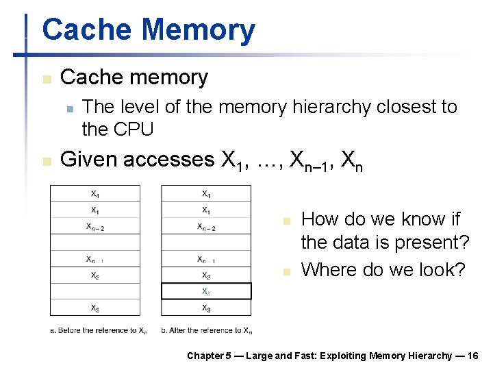
Cache Memory n Cache memory n n The level of the memory hierarchy closest to the CPU Given accesses X 1, …, Xn– 1, Xn n n How do we know if the data is present? Where do we look? Chapter 5 — Large and Fast: Exploiting Memory Hierarchy — 16

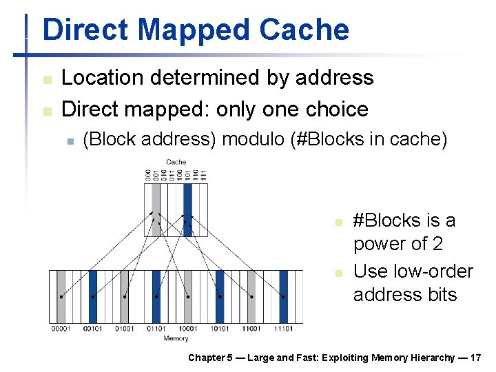
Direct Mapped Cache n n Location determined by address Direct mapped: only one choice n (Block address) modulo (#Blocks in cache) n n #Blocks is a power of 2 Use low-order address bits Chapter 5 — Large and Fast: Exploiting Memory Hierarchy — 17

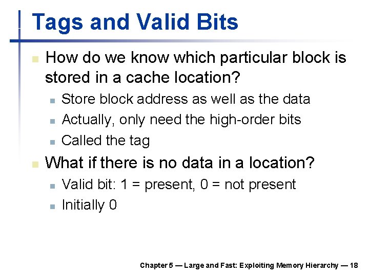
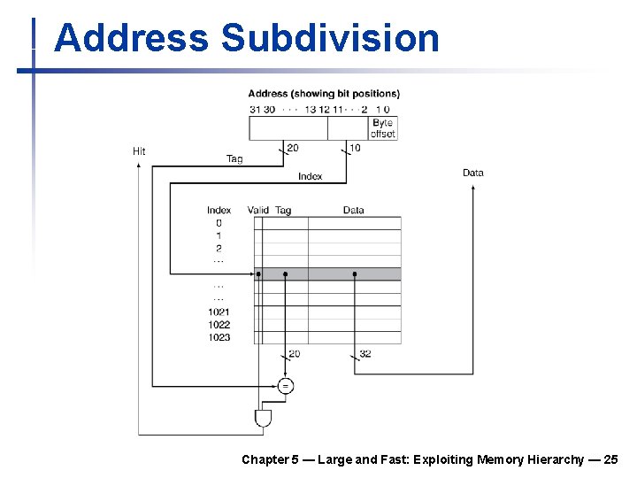
Tags and Valid Bits n How do we know which particular block is stored in a cache location? n n Store block address as well as the data Actually, only need the high-order bits Called the tag What if there is no data in a location? n n Valid bit: 1 = present, 0 = not present Initially 0 Chapter 5 — Large and Fast: Exploiting Memory Hierarchy — 18

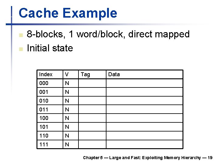
Cache Example n n 8 -blocks, 1 word/block, direct mapped Initial state Index V 000 N 001 N 010 N 011 N 100 N 101 N 110 N 111 N Tag Data Chapter 5 — Large and Fast: Exploiting Memory Hierarchy — 19

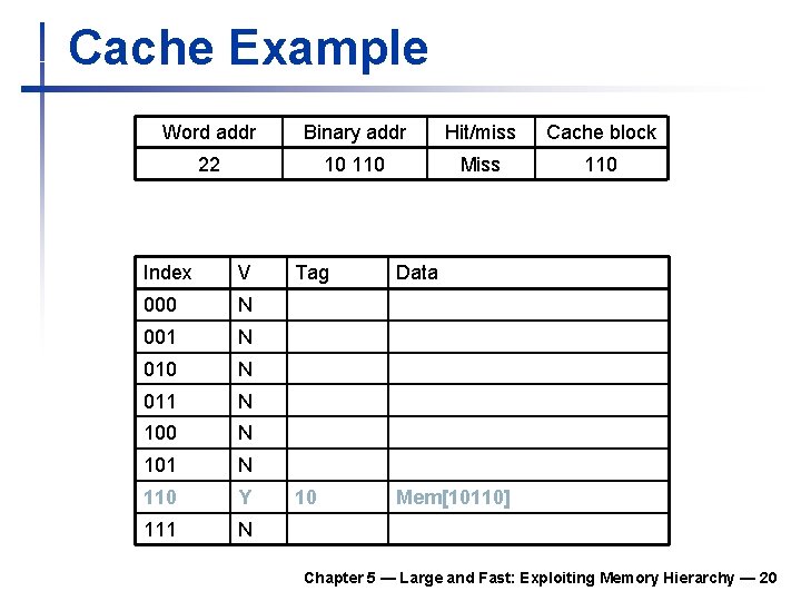
Cache Example Word addr Binary addr Hit/miss Cache block 22 10 110 Miss 110 Index V 000 N 001 N 010 N 011 N 100 N 101 N 110 Y 111 N Tag Data 10 Mem[10110] Chapter 5 — Large and Fast: Exploiting Memory Hierarchy — 20

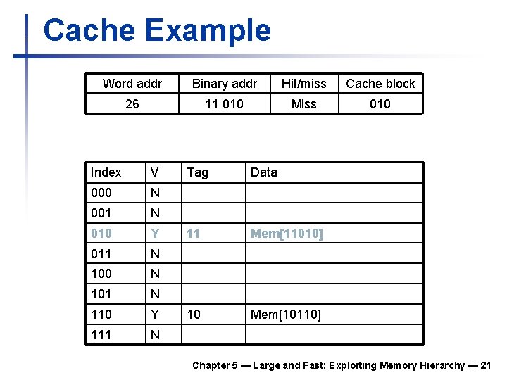
Cache Example Word addr Binary addr Hit/miss Cache block 26 11 010 Miss 010 Index V 000 N 001 N 010 Y 011 N 100 N 101 N 110 Y 111 N Tag Data 11 Mem[11010] 10 Mem[10110] Chapter 5 — Large and Fast: Exploiting Memory Hierarchy — 21

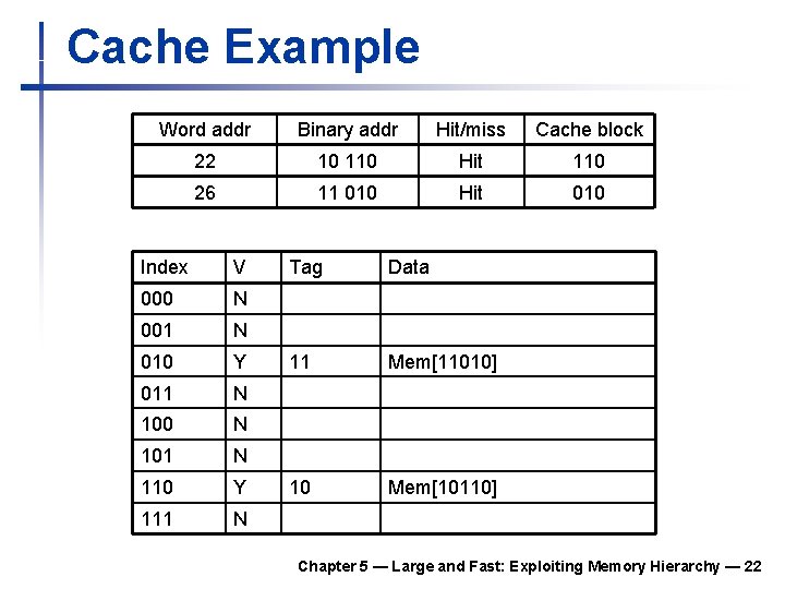
Cache Example Word addr Binary addr Hit/miss Cache block 22 10 110 Hit 110 26 11 010 Hit 010 Index V 000 N 001 N 010 Y 011 N 100 N 101 N 110 Y 111 N Tag Data 11 Mem[11010] 10 Mem[10110] Chapter 5 — Large and Fast: Exploiting Memory Hierarchy — 22

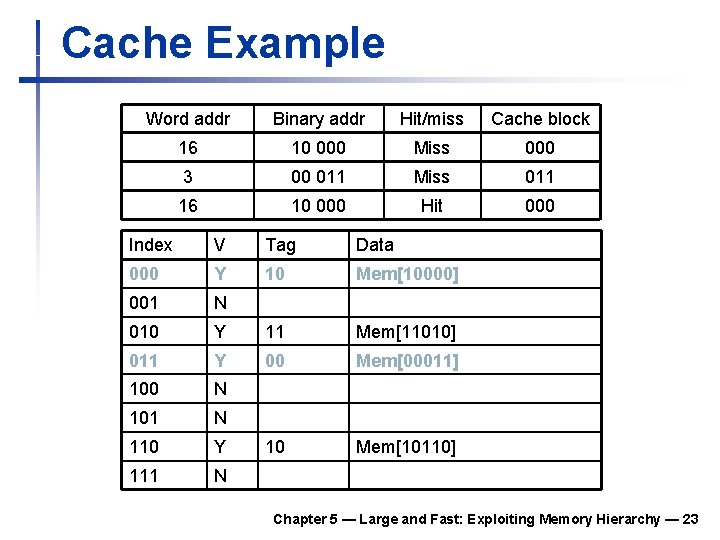
Cache Example Word addr Binary addr Hit/miss Cache block 16 10 000 Miss 000 3 00 011 Miss 011 16 10 000 Hit 000 Index V Tag Data 000 Y 10 Mem[10000] 001 N 010 Y 11 Mem[11010] 011 Y 00 Mem[00011] 100 N 101 N 110 Y 10 Mem[10110] 111 N Chapter 5 — Large and Fast: Exploiting Memory Hierarchy — 23

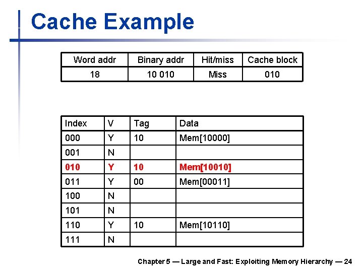
Cache Example Word addr Binary addr Hit/miss Cache block 18 10 010 Miss 010 Index V Tag Data 000 Y 10 Mem[10000] 001 N 010 Y 10 Mem[10010] 011 Y 00 Mem[00011] 100 N 101 N 110 Y 10 Mem[10110] 111 N Chapter 5 — Large and Fast: Exploiting Memory Hierarchy — 24

Address Subdivision Chapter 5 — Large and Fast: Exploiting Memory Hierarchy — 25

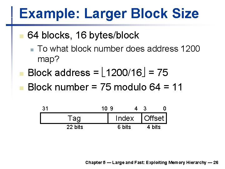
Example: Larger Block Size n 64 blocks, 16 bytes/block n n n To what block number does address 1200 map? Block address = 1200/16 = 75 Block number = 75 modulo 64 = 11 31 10 9 4 3 0 Tag Index Offset 22 bits 6 bits 4 bits Chapter 5 — Large and Fast: Exploiting Memory Hierarchy — 26

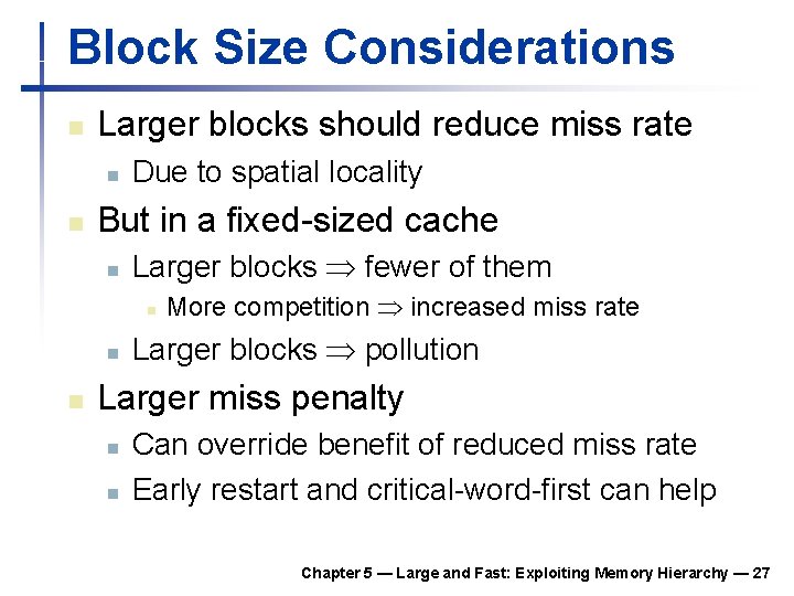
Block Size Considerations n Larger blocks should reduce miss rate n n Due to spatial locality But in a fixed-sized cache n Larger blocks fewer of them n n n More competition increased miss rate Larger blocks pollution Larger miss penalty n n Can override benefit of reduced miss rate Early restart and critical-word-first can help Chapter 5 — Large and Fast: Exploiting Memory Hierarchy — 27

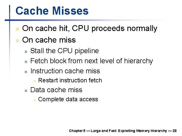
Cache Misses n n On cache hit, CPU proceeds normally On cache miss n n n Stall the CPU pipeline Fetch block from next level of hierarchy Instruction cache miss n n Restart instruction fetch Data cache miss n Complete data access Chapter 5 — Large and Fast: Exploiting Memory Hierarchy — 28

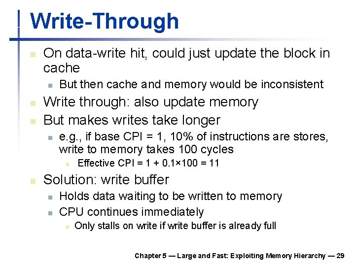
Write-Through n On data-write hit, could just update the block in cache n n n But then cache and memory would be inconsistent Write through: also update memory But makes writes take longer n e. g. , if base CPI = 1, 10% of instructions are stores, write to memory takes 100 cycles n n Effective CPI = 1 + 0. 1× 100 = 11 Solution: write buffer n n Holds data waiting to be written to memory CPU continues immediately n Only stalls on write if write buffer is already full Chapter 5 — Large and Fast: Exploiting Memory Hierarchy — 29

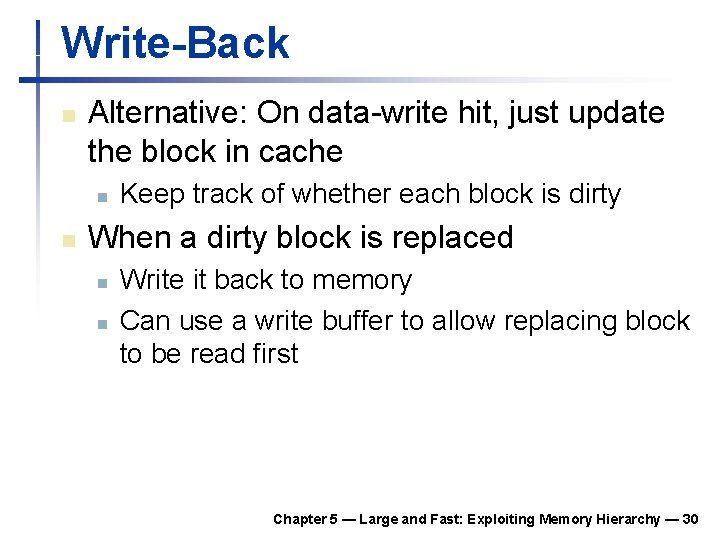
Write-Back n Alternative: On data-write hit, just update the block in cache n n Keep track of whether each block is dirty When a dirty block is replaced n n Write it back to memory Can use a write buffer to allow replacing block to be read first Chapter 5 — Large and Fast: Exploiting Memory Hierarchy — 30

Write Allocation n n What should happen on a write miss? Alternatives for write-through n n Allocate on miss: fetch the block Write around: don’t fetch the block n n Since programs often write a whole block before reading it (e. g. , initialization) For write-back n Usually fetch the block Chapter 5 — Large and Fast: Exploiting Memory Hierarchy — 31

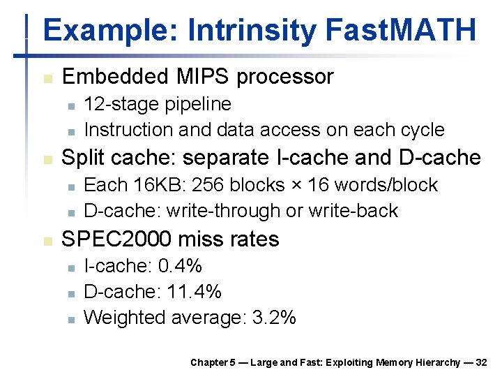
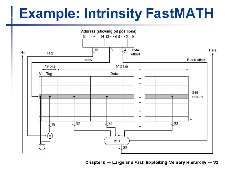
Example: Intrinsity Fast. MATH n Embedded MIPS processor n n n Split cache: separate I-cache and D-cache n n n 12 -stage pipeline Instruction and data access on each cycle Each 16 KB: 256 blocks × 16 words/block D-cache: write-through or write-back SPEC 2000 miss rates n n n I-cache: 0. 4% D-cache: 11. 4% Weighted average: 3. 2% Chapter 5 — Large and Fast: Exploiting Memory Hierarchy — 32

Example: Intrinsity Fast. MATH Chapter 5 — Large and Fast: Exploiting Memory Hierarchy — 33

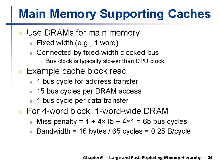
Main Memory Supporting Caches n Use DRAMs for main memory n n Fixed width (e. g. , 1 word) Connected by fixed-width clocked bus n n Example cache block read n n Bus clock is typically slower than CPU clock 1 bus cycle for address transfer 15 bus cycles per DRAM access 1 bus cycle per data transfer For 4 -word block, 1 -word-wide DRAM n n Miss penalty = 1 + 4× 15 + 4× 1 = 65 bus cycles Bandwidth = 16 bytes / 65 cycles = 0. 25 B/cycle Chapter 5 — Large and Fast: Exploiting Memory Hierarchy — 34