Computer Organization and Architecture Internal Memory Outline Internal


- Slides: 49

Computer Organization and Architecture + Internal Memory

+ Outline Internal Memory Semiconductor main memory Organization DRAM and SRAM Types of ROM Chip logic Chip packaging Module organization Interleaved memory Error correction Hard failure Soft error Hamming code

+ Semiconductor Memory Types In earlier computers, the most common form of random-access storage for computer main memory employed an array of doughnut-shaped ferromagnetic loops referred to as cores. Main memory was often referred to as core, a term that persists to this day. But the use of microelectronics has long since vanquished the magnetic core memory. Today, the use of semiconductor chips for main memory is almost universal.

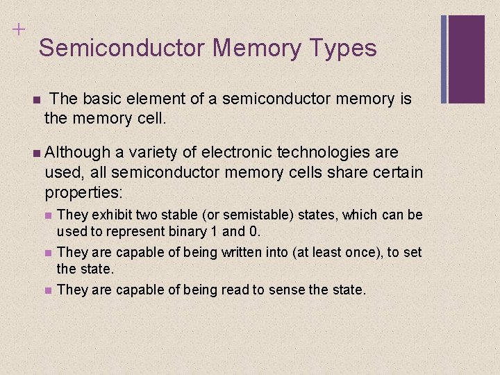
+ Semiconductor Memory Types The basic element of a semiconductor memory is the memory cell. Although a variety of electronic technologies are used, all semiconductor memory cells share certain properties: They exhibit two stable (or semistable) states, which can be used to represent binary 1 and 0. They are capable of being written into (at least once), to set the state. They are capable of being read to sense the state.

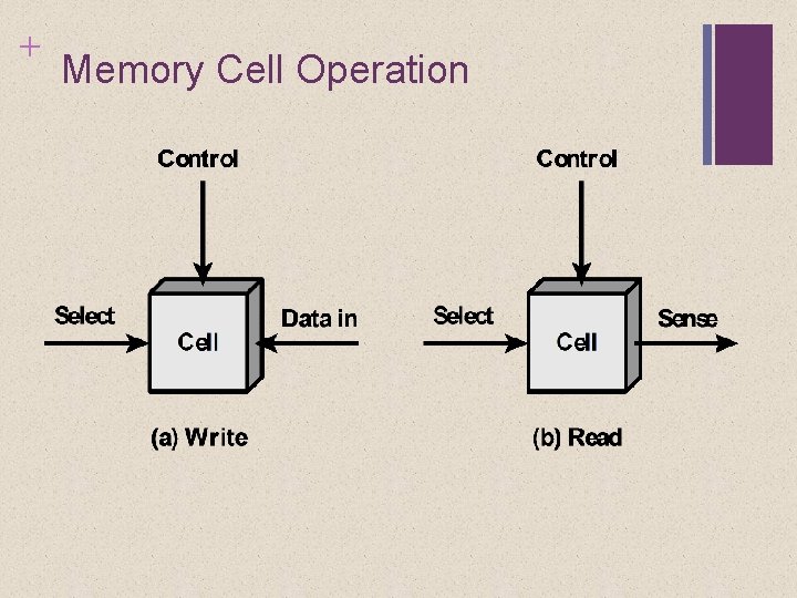
+ Memory Cell Operation

+ Semiconductor Memory Types The cell has three functional terminals capable of carrying an electrical signal. The select terminal selects a memory cell for a read or write operation. The control terminal indicates read or write.

+ Semiconductor Memory Types For writing, the other terminal provides an electrical signal that sets the state of the cell to 1 or 0. For reading, that terminal is used for output of the cell’s state. Individual cells can be selected for reading and writing operations.

Semiconductor Memory Types

+ Semiconductor Memory Types In Random-access memory (RAM) it is possible both to read data from the memory to write new data into the memory easily and rapidly. Both the reading and writing are accomplished through the use of electrical signals.

+ Semiconductor Memory Types The other distinguishing characteristic of RAM is that it is volatile. RAM If must be provided with a constant power supply. the power is interrupted data is lost. RAM The can be used only as temporary storage. two traditional forms of RAM used in computers are: Dynamic RAM (DRAM) Static RAM (SRAM)

+ Dynamic RAM (DRAM) Made with cells that store data as charge on capacitors Presence or absence of charge in a capacitor is interpreted as a binary 1 or 0 Requires periodic charge refreshing to maintain data storage The term dynamic refers to tendency of the stored charge to leak away, even with power continuously applied.

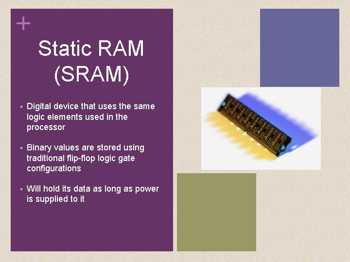
+ Static RAM (SRAM) Digital device that uses the same logic elements used in the processor Binary values are stored using traditional flip-flop logic gate configurations Will hold its data as long as power is supplied to it

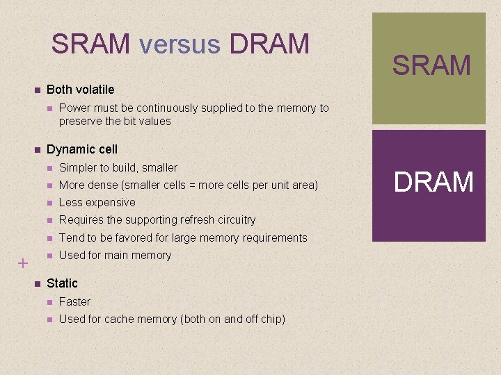
SRAM versus DRAM Both volatile + SRAM Power must be continuously supplied to the memory to preserve the bit values Dynamic cell Simpler to build, smaller More dense (smaller cells = more cells per unit area) Less expensive Requires the supporting refresh circuitry Tend to be favored for large memory requirements Used for main memory Static Faster Used for cache memory (both on and off chip) DRAM

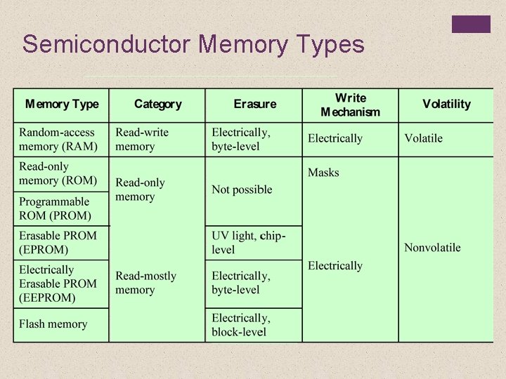
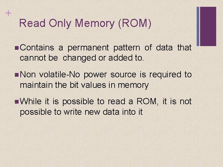
+ Read Only Memory (ROM) Contains a permanent pattern of data that cannot be changed or added to. Non volatile-No power source is required to maintain the bit values in memory While it is possible to read a ROM, it is not possible to write new data into it

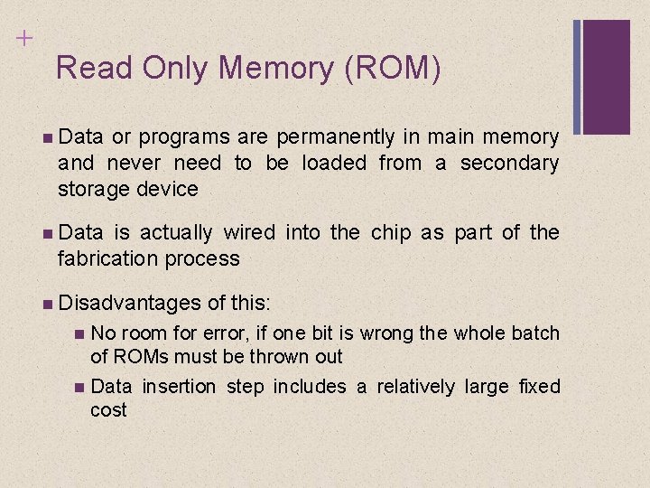
+ Read Only Memory (ROM) Data or programs are permanently in main memory and never need to be loaded from a secondary storage device Data is actually wired into the chip as part of the fabrication process Disadvantages of this: No room for error, if one bit is wrong the whole batch of ROMs must be thrown out Data insertion step includes a relatively large fixed cost

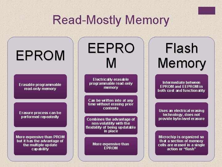
+ Programmable ROM (PROM) Less expensive alternative Nonvolatile and may be written into only once Writing process is performed electrically and may be performed by supplier or customer at a time later than the original chip fabrication Special equipment is required for the writing process Provides Attractive flexibility and convenience for high volume production runs

Read-Mostly Memory EPROM Erasable programmable read-only memory EEPRO M Electrically erasable programmable read-only memory Can be written into at any time without erasing prior contents Erasure process can be performed repeatedly More expensive than PROM but it has the advantage of the multiple update capability Combines the advantage of non-volatility with the flexibility of being updatable in place More expensive than EPROM Flash Memory Intermediate between EPROM and EEPROM in both cost and functionality Uses an electrical erasing technology, does not provide byte-level erasure Microchip is organized so that a section of memory cells are erased in a single action or “flash”

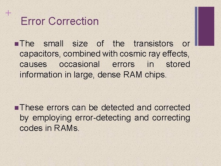
+ Error Correction The small size of the transistors or capacitors, combined with cosmic ray effects, causes occasional errors in stored information in large, dense RAM chips. These errors can be detected and corrected by employing error-detecting and correcting codes in RAMs.

+ Error Correction A semiconductor memory system is subject to errors. These can be categorized as hard failures and soft errors

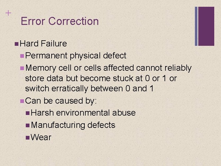
+ Error Correction Hard Failure Permanent physical defect Memory cell or cells affected cannot reliably store data but become stuck at 0 or 1 or switch erratically between 0 and 1 Can be caused by: Harsh environmental abuse Manufacturing defects Wear

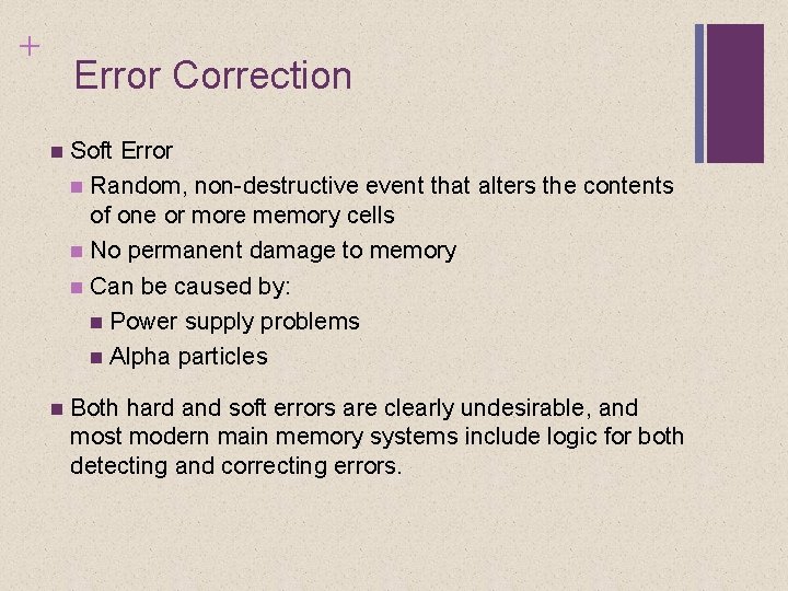
+ Error Correction Soft Error Random, non-destructive event that alters the contents of one or more memory cells No permanent damage to memory Can be caused by: Power supply problems Alpha particles Both hard and soft errors are clearly undesirable, and most modern main memory systems include logic for both detecting and correcting errors.

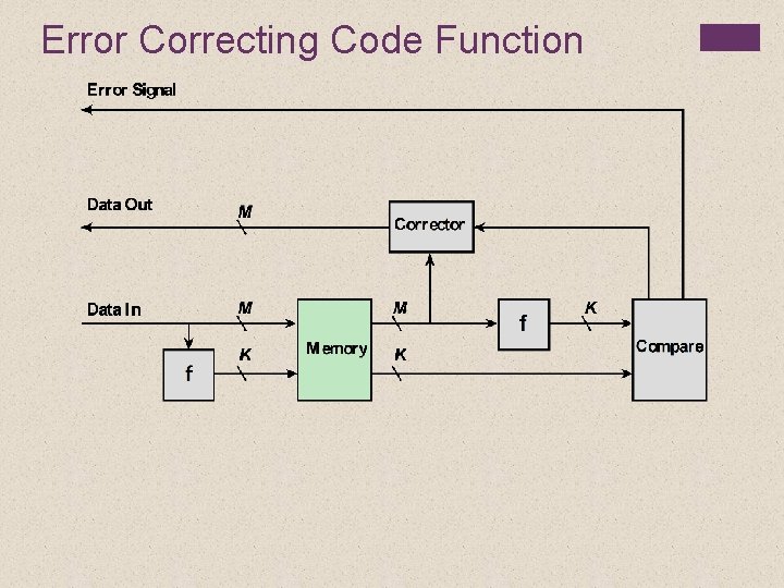
Error Correcting Code Function

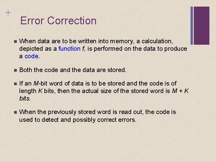
+ Error Correction When data are to be written into memory, a calculation, depicted as a function f, is performed on the data to produce a code. Both the code and the data are stored. If an M-bit word of data is to be stored and the code is of length K bits, then the actual size of the stored word is M + K bits. When the previously stored word is read out, the code is used to detect and possibly correct errors.

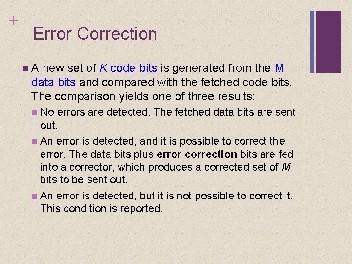
+ Error Correction A new set of K code bits is generated from the M data bits and compared with the fetched code bits. The comparison yields one of three results: No errors are detected. The fetched data bits are sent out. An error is detected, and it is possible to correct the error. The data bits plus error correction bits are fed into a corrector, which produces a corrected set of M bits to be sent out. An error is detected, but it is not possible to correct it. This condition is reported.

+ Error Correction Codes that operate in this fashion are referred to as error-correcting codes. A code is characterized by the number of bit errors in a word that it can correct and detect.

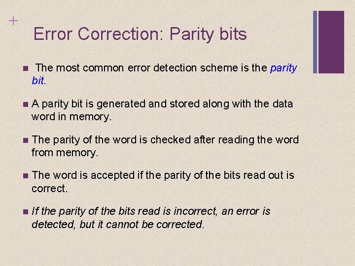
+ Error Correction: Parity bits The most common error detection scheme is the parity bit. A parity bit is generated and stored along with the data word in memory. The parity of the word is checked after reading the word from memory. The word is accepted if the parity of the bits read out is correct. If the parity of the bits read is incorrect, an error is detected, but it cannot be corrected.

+ Hamming codes The most common types of error-correcting codes used in RAM are based on the codes devised by R. W. Hamming. In the Hamming code, k parity bits are added to an M -bit data word, forming a new word of M+k bits.

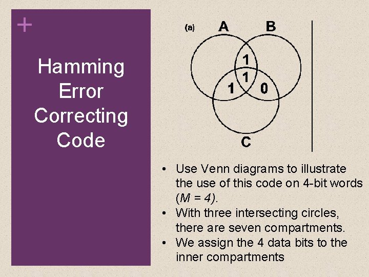
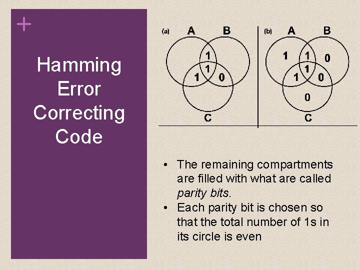
+ Hamming Error Correcting Code • Use Venn diagrams to illustrate the use of this code on 4 -bit words (M = 4). • With three intersecting circles, there are seven compartments. • We assign the 4 data bits to the inner compartments

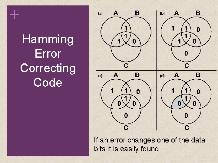
+ Hamming Error Correcting Code • The remaining compartments are filled with what are called parity bits. • Each parity bit is chosen so that the total number of 1 s in its circle is even

+ Hamming Error Correcting Code If an error changes one of the data bits it is easily found.

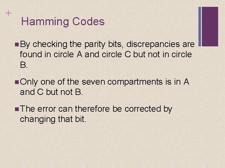
+ Hamming Codes By checking the parity bits, discrepancies are found in circle A and circle C but not in circle B. Only one of the seven compartments is in A and C but not B. The error can therefore be corrected by changing that bit.

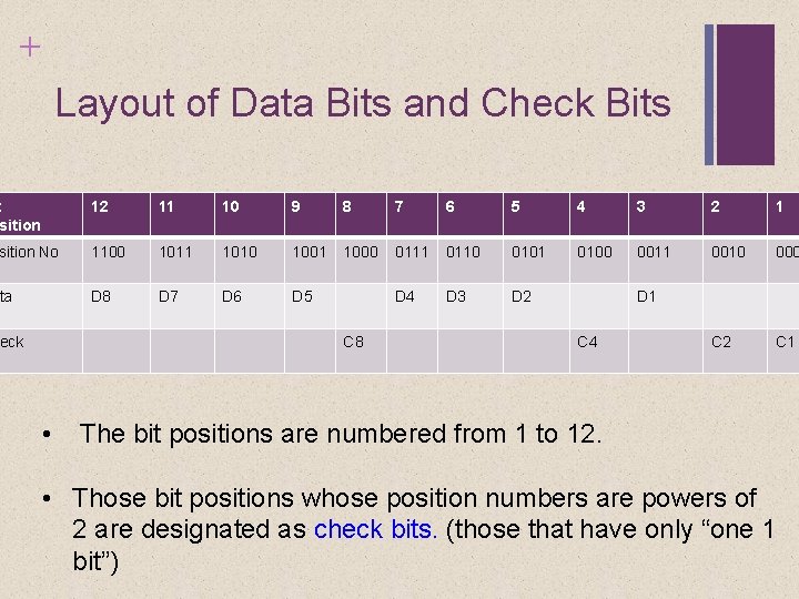
+ Hamming codes To clarify the concepts involved, we will develop a code that can detect and correct single-bit errors in 8 -bit words. In the Hamming code, k parity bits are added to an M-bit data word, forming a new word of M+k bits. The bit positions are numbered in sequence from 1 to M+k.

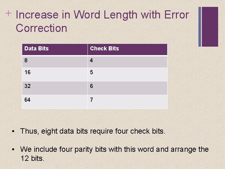
+ Increase in Word Length with Error Correction Data Bits Check Bits 8 4 16 5 32 6 64 7 • Thus, eight data bits require four check bits. • We include four parity bits with this word and arrange the 12 bits.

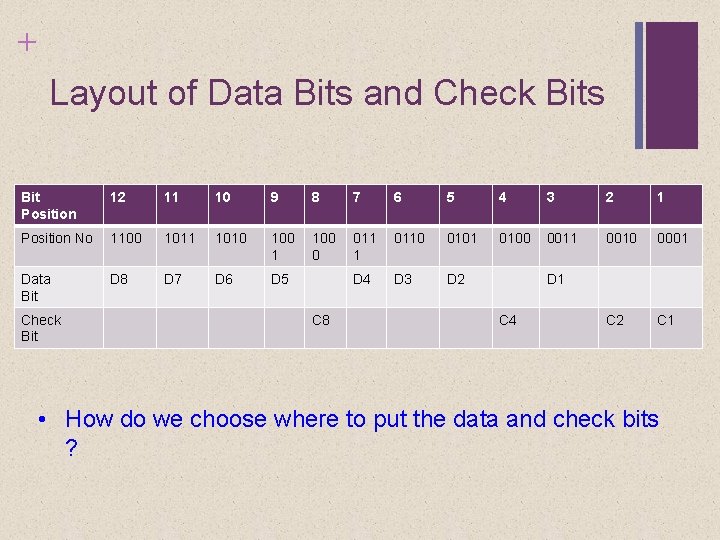
+ Layout of Data Bits and Check Bits Bit Position 12 11 10 9 8 7 6 5 4 3 2 1 Position No 1100 1011 1010 100 1 100 0 011 1 0110 0101 0100 0011 0010 0001 Data Bit D 8 D 7 D 6 D 5 D 4 D 3 D 2 C 1 Check Bit C 8 D 1 C 4 • How do we choose where to put the data and check bits ?

+ Layout of Data Bits and Check Bits t sition 12 11 10 9 8 7 6 5 4 3 2 1 sition No 1100 1011 1010 1001 1000 0111 0110 0101 0100 0011 0010 000 ta D 8 D 7 D 6 D 5 D 4 D 3 D 2 C 1 eck C 8 • D 1 C 4 The bit positions are numbered from 1 to 12. • Those bit positions whose position numbers are powers of 2 are designated as check bits. (those that have only “one 1 bit”)

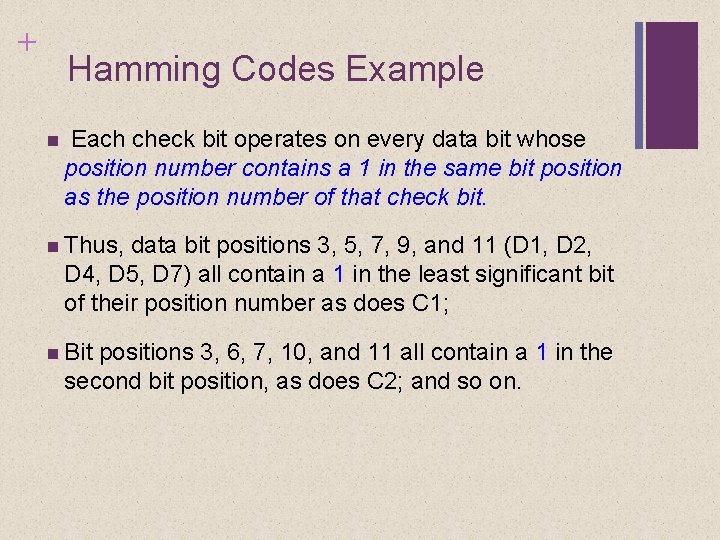
+ Hamming Codes Example Each check bit operates on every data bit whose position number contains a 1 in the same bit position as the position number of that check bit. Thus, data bit positions 3, 5, 7, 9, and 11 (D 1, D 2, D 4, D 5, D 7) all contain a 1 in the least significant bit of their position number as does C 1; Bit positions 3, 6, 7, 10, and 11 all contain a 1 in the second bit position, as does C 2; and so on.

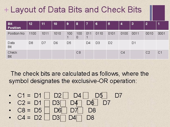
+ Layout of Data Bits and Check Bits Bit Position 12 11 10 9 8 7 6 5 4 3 2 1 Position No 1100 1011 1010 100 1 100 0 011 1 0110 0101 0100 0011 0010 0001 Data Bit D 8 D 7 D 6 D 5 D 4 D 3 D 2 C 1 Check Bit C 8 D 1 C 4 The check bits are calculated as follows, where the symbol designates the exclusive-OR operation: • • C 1 = C 2 = C 8 = C 4 = D 1 D 5 D 2 D 3 D 6 D 3 D 4 D 5 D 7 D 4 D 6 D 7 D 8 D 4 D 8

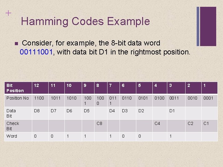
+ Hamming Codes Example Consider, for example, the 8 -bit data word 00111001, with data bit D 1 in the rightmost position. Bit Position 12 11 10 9 8 7 6 5 4 3 2 1 Position No 1100 1011 1010 100 1 100 0 011 1 0110 0101 0100 0011 0010 0001 Data Bit D 8 D 7 D 6 D 5 D 4 D 3 D 2 C 1 Check Bit Word C 8 0 0 1 1 D 1 C 4 1 0 0 1

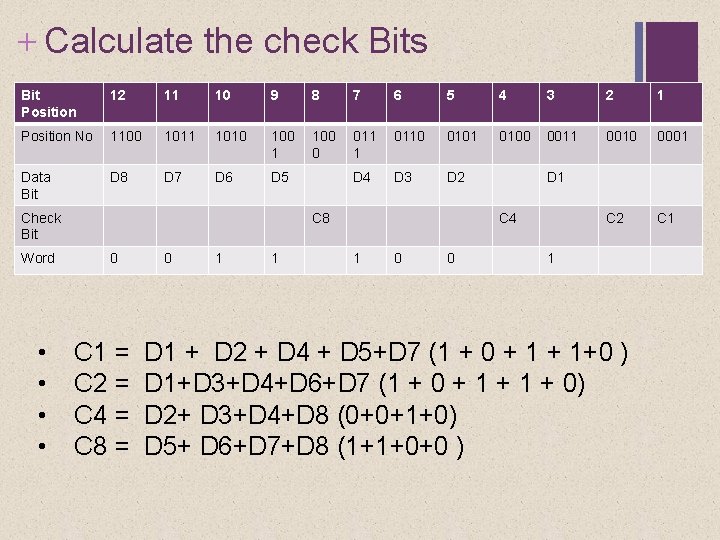
+ Calculate the check Bits Bit Position 12 11 10 9 8 7 6 5 4 3 2 1 Position No 1100 1011 1010 100 1 100 0 011 1 0110 0101 0100 0011 0010 0001 Data Bit D 8 D 7 D 6 D 5 D 4 D 3 D 2 C 1 Check Bit Word • • C 8 0 C 1 = C 2 = C 4 = C 8 = 0 1 1 D 1 C 4 1 0 0 1 D 1 + D 2 + D 4 + D 5+D 7 (1 + 0 + 1+0 ) D 1+D 3+D 4+D 6+D 7 (1 + 0 + 1 + 0) D 2+ D 3+D 4+D 8 (0+0+1+0) D 5+ D 6+D 7+D 8 (1+1+0+0 )

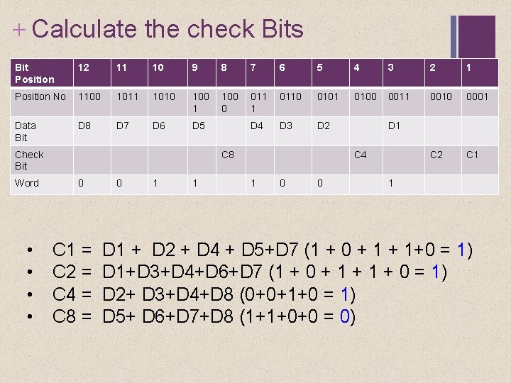
+ Calculate the check Bits Bit Position 12 11 10 9 8 7 6 5 4 3 2 1 Position No 1100 1011 1010 100 1 100 0 011 1 0110 0101 0100 0011 0010 0001 Data Bit D 8 D 7 D 6 D 5 D 4 D 3 D 2 C 1 Check Bit Word • • C 8 0 C 1 = C 2 = C 4 = C 8 = 0 1 1 D 1 C 4 1 0 0 1 D 1 + D 2 + D 4 + D 5+D 7 (1 + 0 + 1+0 = 1) D 1+D 3+D 4+D 6+D 7 (1 + 0 + 1 + 0 = 1) D 2+ D 3+D 4+D 8 (0+0+1+0 = 1) D 5+ D 6+D 7+D 8 (1+1+0+0 = 0)

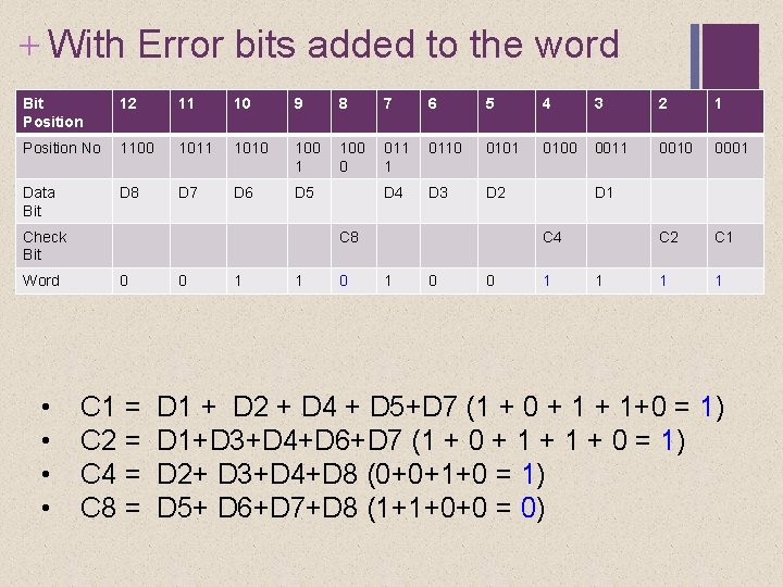
+ With Error bits added to the word Bit Position 12 11 10 9 8 7 6 5 4 3 2 1 Position No 1100 1011 1010 100 1 100 0 011 1 0110 0101 0100 0011 0010 0001 Data Bit D 8 D 7 D 6 D 5 D 4 D 3 D 2 C 1 1 1 Check Bit Word • • C 8 0 C 1 = C 2 = C 4 = C 8 = 0 1 1 0 D 1 C 4 1 0 0 1 1 D 1 + D 2 + D 4 + D 5+D 7 (1 + 0 + 1+0 = 1) D 1+D 3+D 4+D 6+D 7 (1 + 0 + 1 + 0 = 1) D 2+ D 3+D 4+D 8 (0+0+1+0 = 1) D 5+ D 6+D 7+D 8 (1+1+0+0 = 0)

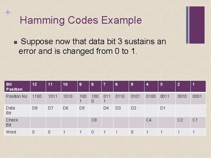
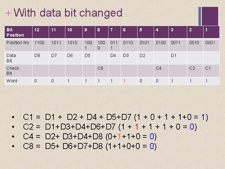
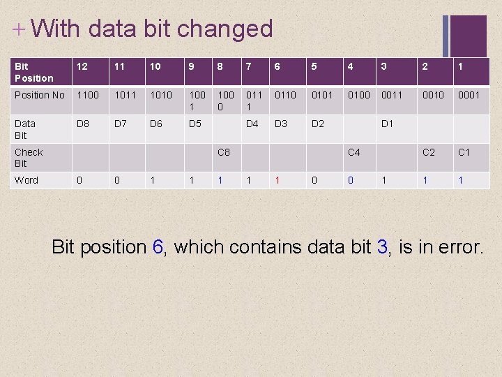
+ Hamming Codes Example Suppose now that data bit 3 sustains an error and is changed from 0 to 1. Bit Position 12 11 10 9 8 7 6 5 4 3 2 1 Position No 1100 1011 1010 100 1 100 0 011 1 0110 0101 0100 0011 0010 0001 Data Bit D 8 D 7 D 6 D 5 D 4 D 3 D 2 C 1 1 1 Check Bit Word C 8 0 0 1 1 0 D 1 C 4 1 1 0 1 1

+ With data bit changed Bit Position 12 11 10 9 8 7 6 5 4 3 2 1 Position No 1100 1011 1010 100 1 100 0 011 1 0110 0101 0100 0011 0010 0001 Data Bit D 8 D 7 D 6 D 5 D 4 D 3 D 2 C 1 1 1 Check Bit Word • • C 8 0 C 1 = C 2 = C 4 = C 8 = 0 1 1 1 D 1 C 4 1 1 0 0 1 D 1 + D 2 + D 4 + D 5+D 7 (1 + 0 + 1+0 = 1) D 1+D 3+D 4+D 6+D 7 (1 + 1 + 0 = 0) D 2+ D 3+D 4+D 8 (0+1+1+0 = 0) D 5+ D 6+D 7+D 8 (1+1+0+0 = 0)

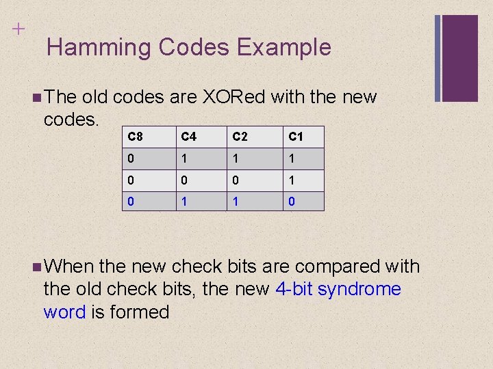
+ Hamming Codes Example The old codes are XORed with the new codes. When C 8 C 4 C 2 C 1 0 1 1 1 0 0 0 1 1 0 the new check bits are compared with the old check bits, the new 4 -bit syndrome word is formed

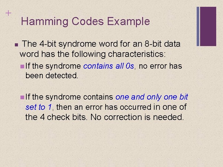
+ Hamming Codes Example The 4 -bit syndrome word for an 8 -bit data word has the following characteristics: If the syndrome contains all 0 s, no error has been detected. If the syndrome contains one and only one bit set to 1, then an error has occurred in one of the 4 check bits. No correction is needed.

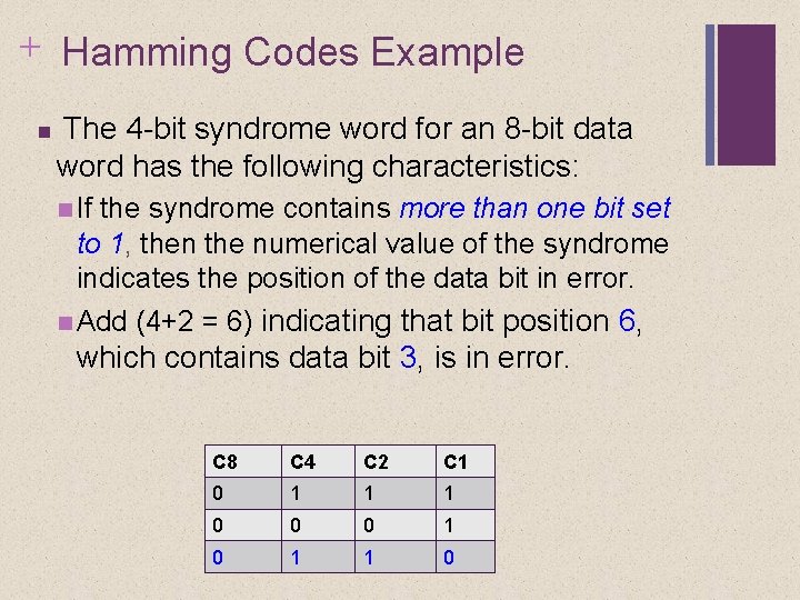
+ Hamming Codes Example The 4 -bit syndrome word for an 8 -bit data word has the following characteristics: If the syndrome contains more than one bit set to 1, then the numerical value of the syndrome indicates the position of the data bit in error. Add (4+2 = 6) indicating that bit position 6, which contains data bit 3, is in error. C 8 C 4 C 2 C 1 0 1 1 1 0 0 0 1 1 0

+ With data bit changed Bit Position 12 11 10 9 8 7 6 5 4 3 2 1 Position No 1100 1011 1010 100 1 100 0 011 1 0110 0101 0100 0011 0010 0001 Data Bit D 8 D 7 D 6 D 5 D 4 D 3 D 2 C 1 1 1 Check Bit Word C 8 0 0 1 1 1 D 1 C 4 1 1 0 0 1 Bit position 6, which contains data bit 3, is in error.

+ Summary Internal Memory Semiconductor main memory Organization DRAM and SRAM Types of ROM Chip logic Chip packaging Module organization Interleaved memory Error correction Hard failure Soft error Hamming code

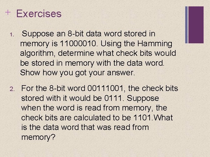
+ Exercises 1. Suppose an 8 -bit data word stored in memory is 11000010. Using the Hamming algorithm, determine what check bits would be stored in memory with the data word. Show you got your answer. 2. For the 8 -bit word 00111001, the check bits stored with it would be 0111. Suppose when the word is read from memory, the check bits are calculated to be 1101. What is the data word that was read from memory?