Computer Organization 3 Fundamental Components of Computer The




- Slides: 66

Computer Organization

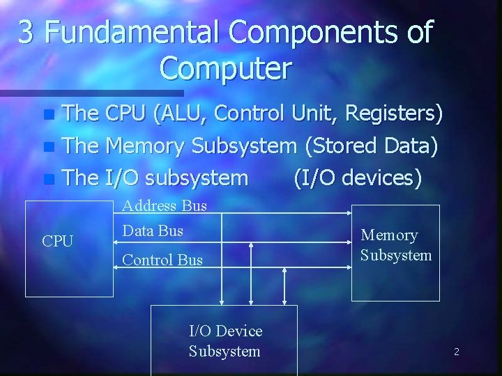
3 Fundamental Components of Computer The CPU (ALU, Control Unit, Registers) n The Memory Subsystem (Stored Data) n The I/O subsystem (I/O devices) n CPU Address Bus Data Bus Control Bus I/O Device Subsystem Memory Subsystem 2

Each of these Components are connected through Buses. BUS - Physically a set of wires. The components of the Computer are connected to these buses. n Address Bus n Data Bus n Control Bus n 3

Address Bus Used to specify the address of the memory location to access. n Each I/O devices has a unique address. (monitor, mouse, cd-rom) n CPU reads data or instructions from other locations by specifying the address of its location. n CPU always outputs to the address bus 4 and never reads from it. n

Data Bus Actual data is transferred via the data bus. n When the cpu sends an address to memory, the memory will send data via the data bus in return to the cpu. n 5

Control Bus Collection of individual control signals. n Whether the cpu will read or write data. n CPU is accessing memory or an I/O device n Memory or I/O is ready to transfer data n 6

I/O Bus or Local Bus In today’s computers the I/O controller will have an extra bus called the I/O bus. n The I/O bus will be used to access all other I/O devices connected to the system. n Example: PCI bus n 7

Instruction Cycles Procedure the CPU goes through to process an instruction. n 1. Fetch - get instruction n 2. Decode - interperate the instruction n 3. Execute - run the instruction. n 8

CPU organization CPU controls the Computer n The CPU will fetch, decode and execute instructions. n The CPU has three internal sections: register section, ALU and Control Unit n 9

Register Section Includes collection of registers and a bus. n Processor’s instruction set architecture are found in this section. n Non accessible registers by the programmer. These are to be used for registers to latch the address being accessed and a temp storage register. n 10

Arithmetic/Logic Unit (ALU) Performs most Arithmetic and logical operations. n Retrieves and stores its information with the register section of the CPU. n 11

MEMORY ORGANIZATION • Memory Hierarchy • Main Memory • Auxiliary Memory • Associative Memory • Cache Memory • Virtual Memory • Memory Management Hardware` 12

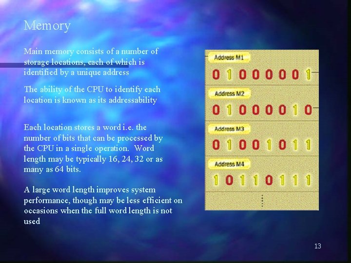
Memory Main memory consists of a number of storage locations, each of which is identified by a unique address The ability of the CPU to identify each location is known as its addressability Each location stores a word i. e. the number of bits that can be processed by the CPU in a single operation. Word length may be typically 16, 24, 32 or as many as 64 bits. A large word length improves system performance, though may be less efficient on occasions when the full word length is not used 13

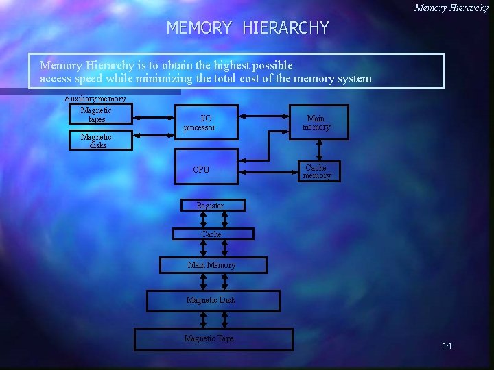
Memory Hierarchy MEMORY HIERARCHY Memory Hierarchy is to obtain the highest possible access speed while minimizing the total cost of the memory system Auxiliary memory Magnetic tapes I/O processor Main memory CPU Cache memory Magnetic disks Register Cache Main Memory Magnetic Disk Magnetic Tape 14

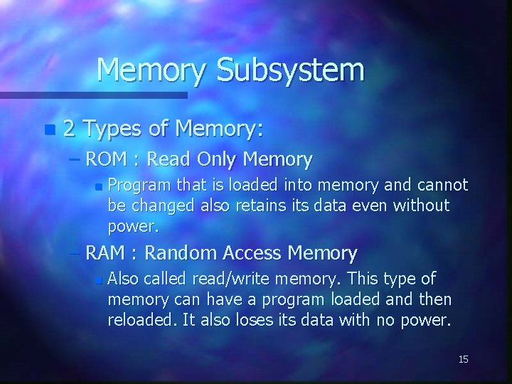
Memory Subsystem n 2 Types of Memory: – ROM : Read Only Memory n Program that is loaded into memory and cannot be changed also retains its data even without power. – RAM : Random Access Memory n Also called read/write memory. This type of memory can have a program loaded and then reloaded. It also loses its data with no power. 15

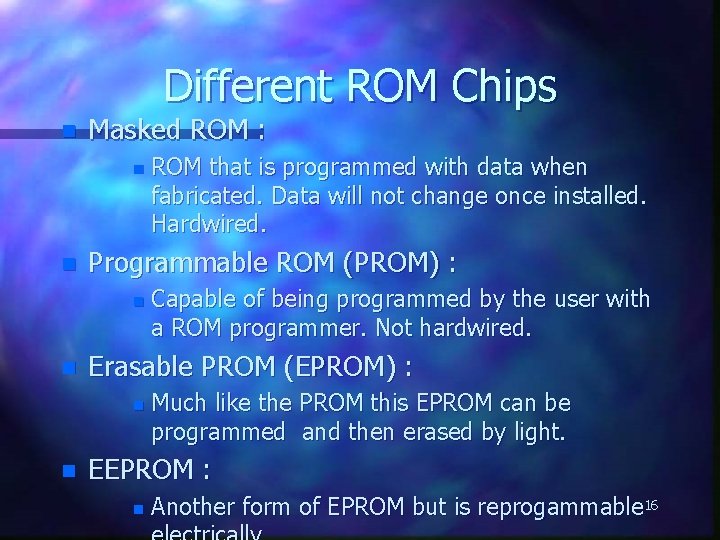
Different ROM Chips n Masked ROM : n n Programmable ROM (PROM) : n n Capable of being programmed by the user with a ROM programmer. Not hardwired. Erasable PROM (EPROM) : n n ROM that is programmed with data when fabricated. Data will not change once installed. Hardwired. Much like the PROM this EPROM can be programmed and then erased by light. EEPROM : n Another form of EPROM but is reprogammable 16

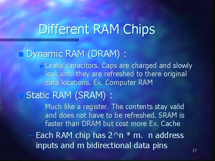
Different RAM Chips n Dynamic RAM (DRAM) : n n Leaky capacitors. Caps are charged and slowly leak until they are refreshed to there original data locations. Ex. Computer RAM Static RAM (SRAM) : n Much like a register. The contents stay valid and does not have to be refreshed. SRAM is faster than DRAM but cost more Ex. Cache – Each RAM chip has 2^n * m. n address inputs and m bidirectional data pins 17

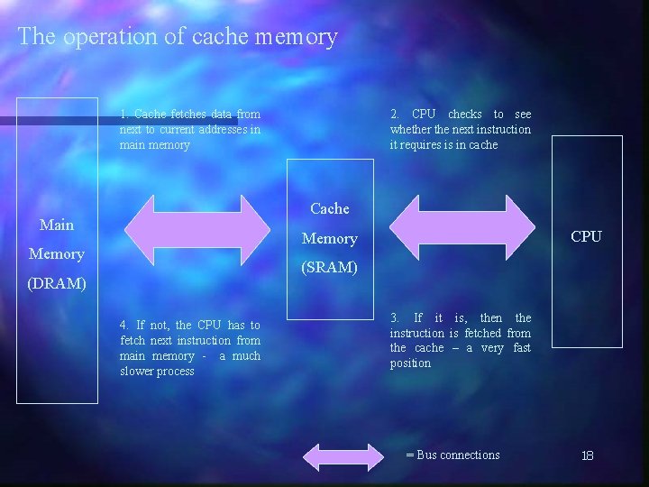
The operation of cache memory 1. Cache fetches data from next to current addresses in main memory 2. CPU checks to see whether the next instruction it requires is in cache Cache Main CPU Memory (SRAM) (DRAM) 4. If not, the CPU has to fetch next instruction from main memory - a much slower process 3. If it is, then the instruction is fetched from the cache – a very fast position = Bus connections 18

Addressing Modes Immediate n Direct n Indirect n Register Indirect n Displacement (Indexed) n Stack n 19

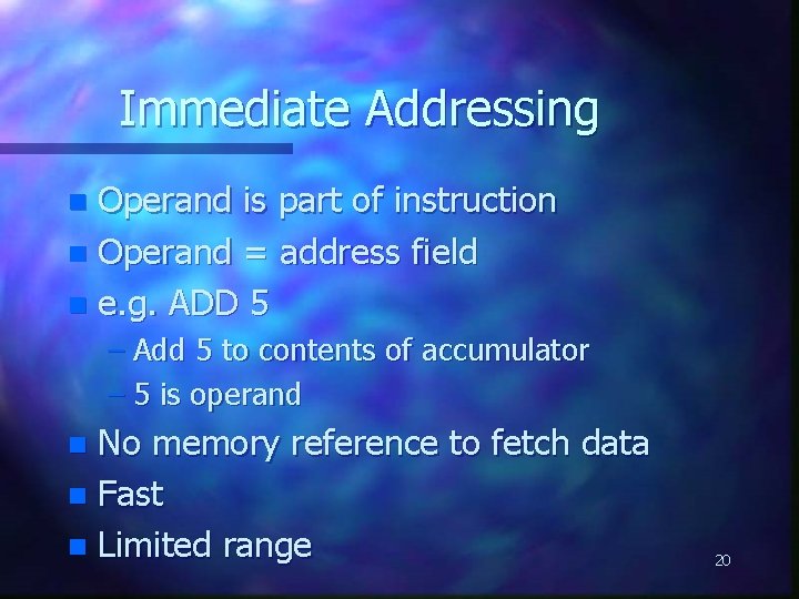
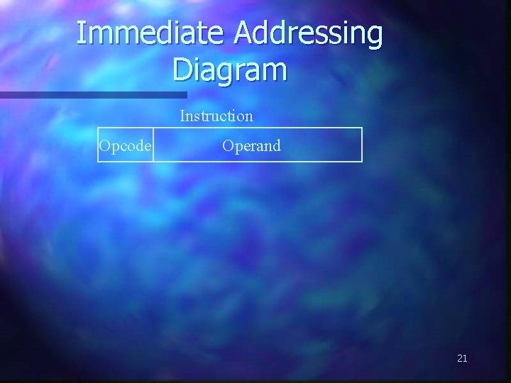
Immediate Addressing Operand is part of instruction n Operand = address field n e. g. ADD 5 n – Add 5 to contents of accumulator – 5 is operand No memory reference to fetch data n Fast n Limited range n 20

Immediate Addressing Diagram Instruction Opcode Operand 21

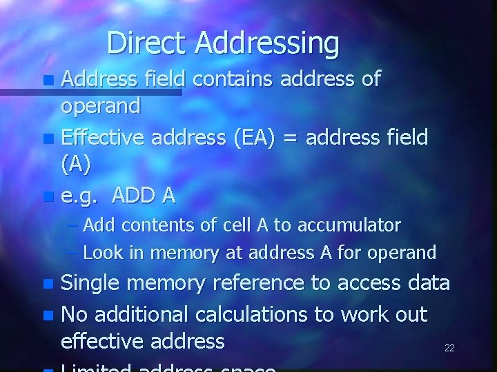
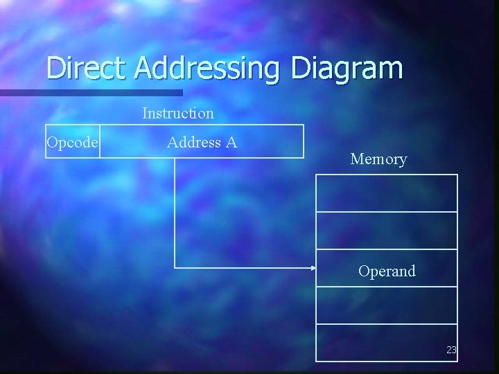
Direct Addressing Address field contains address of operand n Effective address (EA) = address field (A) n e. g. ADD A n – Add contents of cell A to accumulator – Look in memory at address A for operand Single memory reference to access data n No additional calculations to work out effective address 22 n

Direct Addressing Diagram Instruction Opcode Address A Memory Operand 23

Direct Addressing Diagram Instruction Opcode Address A Memory Operand 24

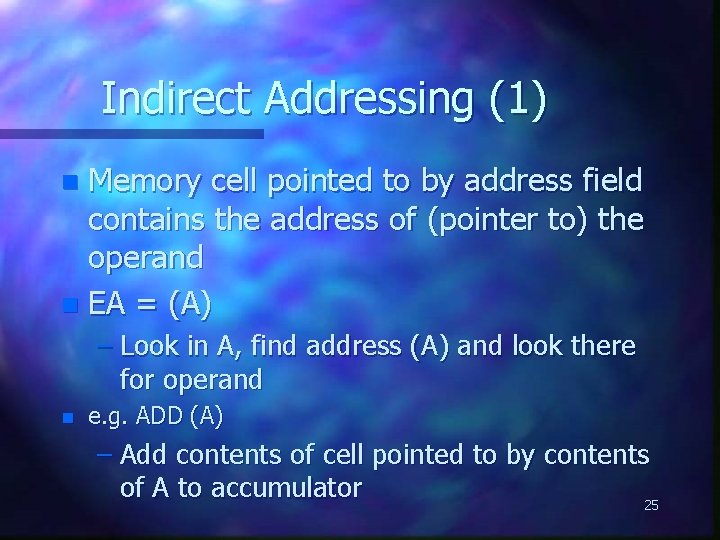
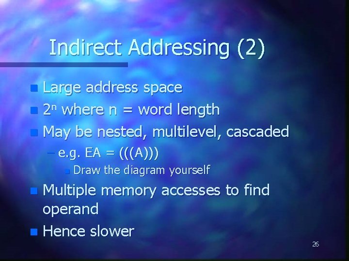
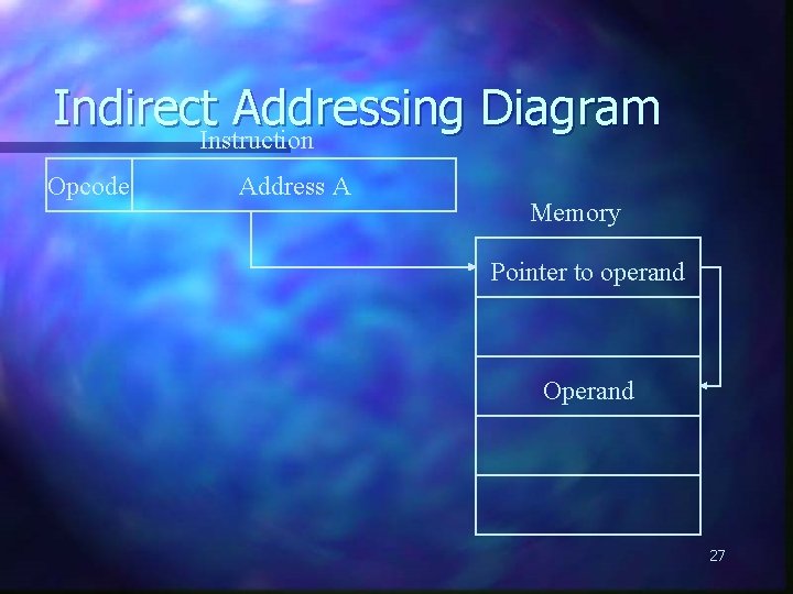
Indirect Addressing (1) Memory cell pointed to by address field contains the address of (pointer to) the operand n EA = (A) n – Look in A, find address (A) and look there for operand n e. g. ADD (A) – Add contents of cell pointed to by contents of A to accumulator 25

Indirect Addressing (2) Large address space n 2 n where n = word length n May be nested, multilevel, cascaded n – e. g. EA = (((A))) n Draw the diagram yourself Multiple memory accesses to find operand n Hence slower n 26

Indirect. Instruction Addressing Diagram Opcode Address A Memory Pointer to operand Operand 27

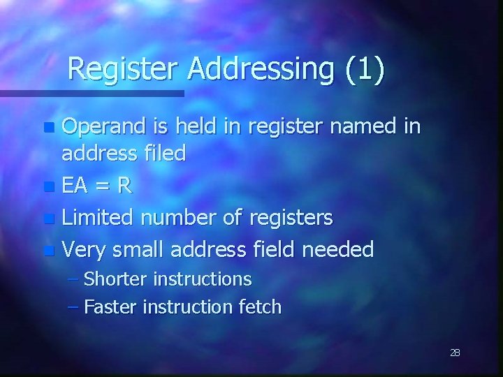
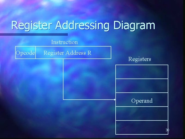
Register Addressing (1) Operand is held in register named in address filed n EA = R n Limited number of registers n Very small address field needed n – Shorter instructions – Faster instruction fetch 28

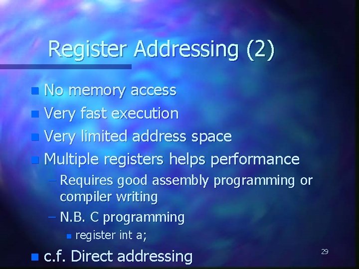
Register Addressing (2) No memory access n Very fast execution n Very limited address space n Multiple registers helps performance n – Requires good assembly programming or compiler writing – N. B. C programming n n register int a; c. f. Direct addressing 29

Register Addressing Diagram Instruction Opcode Register Address R Registers Operand 30

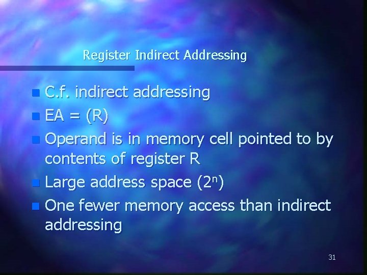
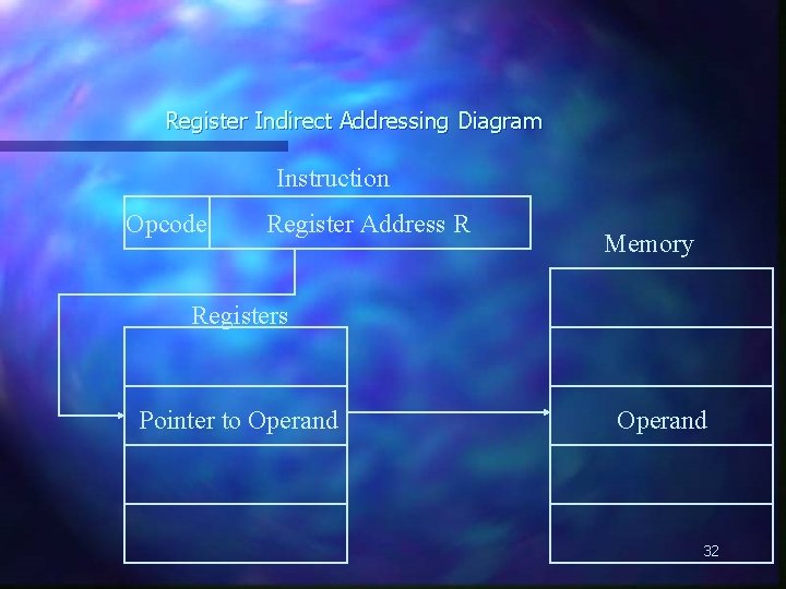
Register Indirect Addressing C. f. indirect addressing n EA = (R) n Operand is in memory cell pointed to by contents of register R n Large address space (2 n) n One fewer memory access than indirect addressing n 31

Register Indirect Addressing Diagram Instruction Opcode Register Address R Memory Registers Pointer to Operand 32

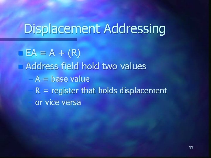
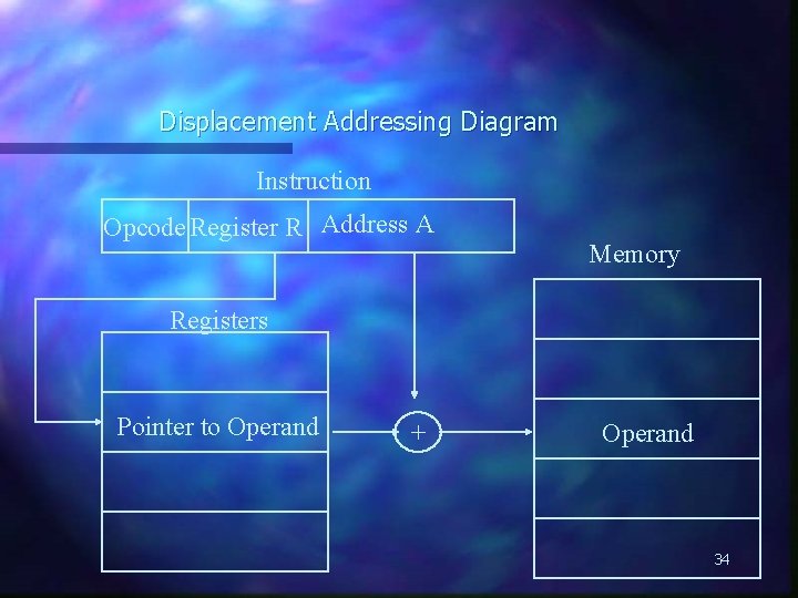
Displacement Addressing EA = A + (R) n Address field hold two values n – A = base value – R = register that holds displacement – or vice versa 33

Displacement Addressing Diagram Instruction Opcode Register R Address A Memory Registers Pointer to Operand + Operand 34

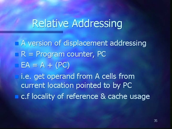
Relative Addressing A version of displacement addressing n R = Program counter, PC n EA = A + (PC) n i. e. get operand from A cells from current location pointed to by PC n c. f locality of reference & cache usage n 35

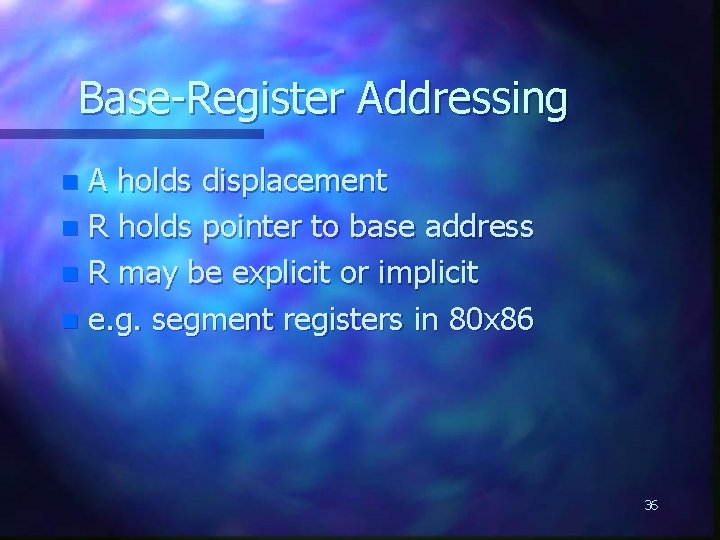
Base-Register Addressing A holds displacement n R holds pointer to base address n R may be explicit or implicit n e. g. segment registers in 80 x 86 n 36

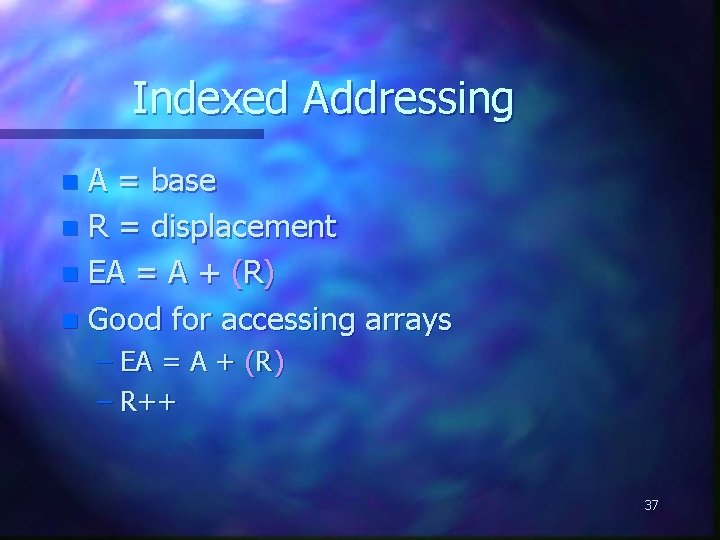
Indexed Addressing A = base n R = displacement n EA = A + (R) n Good for accessing arrays n – EA = A + (R) – R++ 37

Stack Addressing Operand is (implicitly) on top of stack n e. g. n – ADD Pop two items from stack and add 38

Input-Output Organization n 11 -1 Peripheral Devices – I/O Subsystem n Provides an efficient mode of communication between the central system and the outside environment – Peripheral (or I/O Device) n n Input or Output devices attached to the computer 11 -2 Input-Output Interface n 1) A conversion of signal values may be required 39

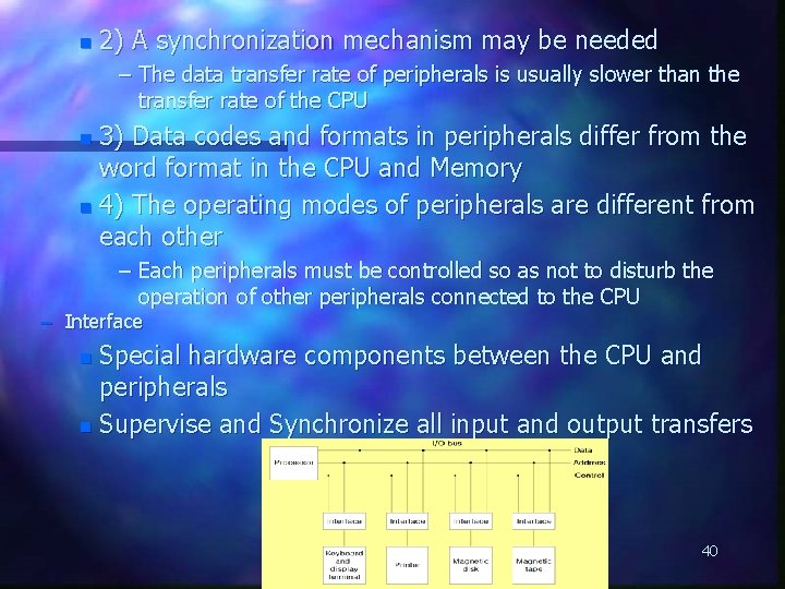
n 2) A synchronization mechanism may be needed – The data transfer rate of peripherals is usually slower than the transfer rate of the CPU 3) Data codes and formats in peripherals differ from the word format in the CPU and Memory n 4) The operating modes of peripherals are different from each other n – Each peripherals must be controlled so as not to disturb the operation of other peripherals connected to the CPU – Interface Special hardware components between the CPU and peripherals n Supervise and Synchronize all input and output transfers n 40

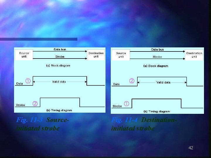
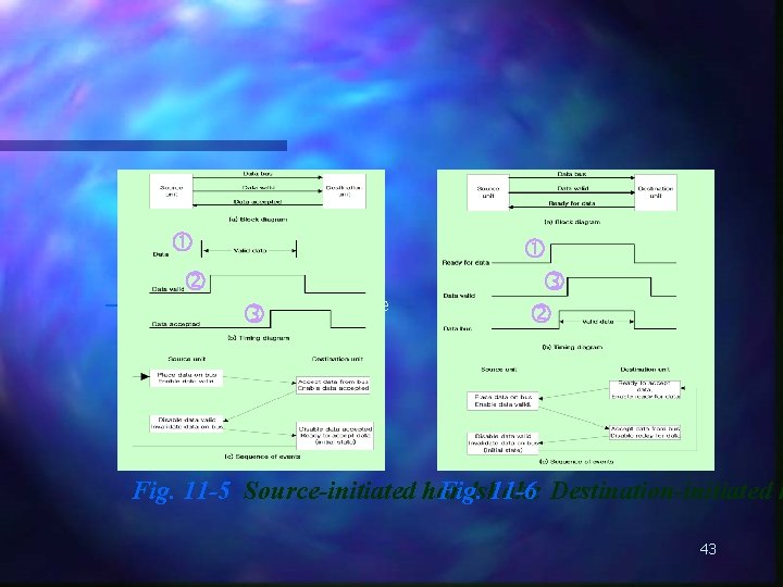
– Transfer – Synchronous Data Transfer All data transfers occur simultaneously during the occurrence of a clock pulse n Registers in the interface share a common clock with CPU registers n – Asynchronous Data Transfer Internal timing in each unit (CPU and Interface) is independent n Each unit uses its own private clock for internal registers n 41

Fig. 11 -3 Sourceinitiated strobe Fig. 11 -4 Destinationinitiated strobe 42

– Handshake : Agreement betwee Fig. 11 -5 Source-initiated handshake Fig. 11 -6 Destination-initiated h 43

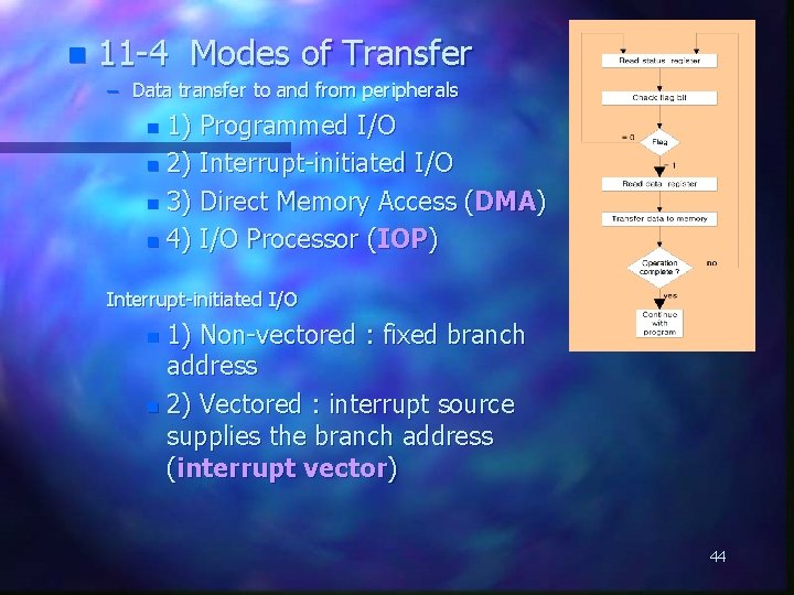
n 11 -4 Modes of Transfer – Data transfer to and from peripherals 1) Programmed I/O n 2) Interrupt-initiated I/O n 3) Direct Memory Access (DMA) n 4) I/O Processor (IOP) n Interrupt-initiated I/O 1) Non-vectored : fixed branch address n 2) Vectored : interrupt source supplies the branch address (interrupt vector) n 44

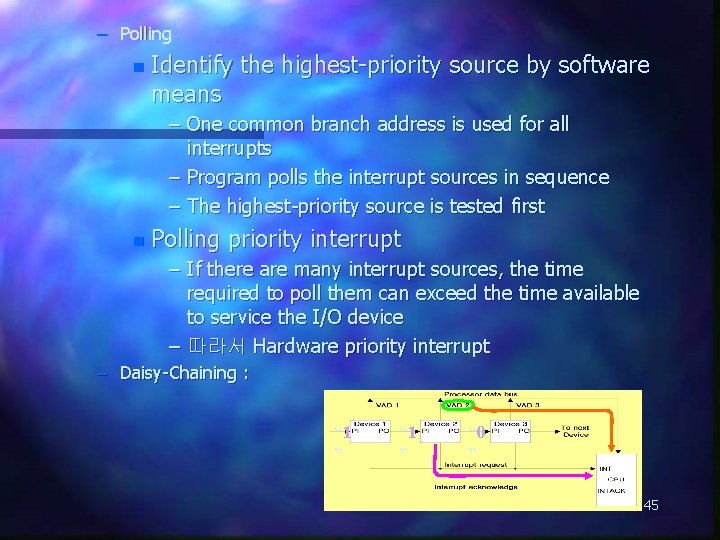
– Polling n Identify the highest-priority source by software means – One common branch address is used for all interrupts – Program polls the interrupt sources in sequence – The highest-priority source is tested first n Polling priority interrupt – If there are many interrupt sources, the time required to poll them can exceed the time available to service the I/O device – 따라서 Hardware priority interrupt – Daisy-Chaining : “ 1 ” “ 0 ” 45

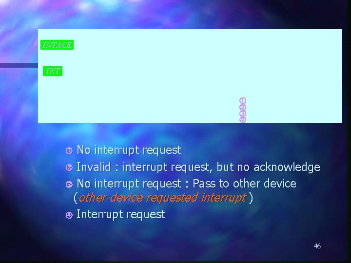
INTACK INT n One stage of the daisy-chain priority arrangement : Fig. 11 -13 No interrupt request Invalid : interrupt request, but no acknowledge No interrupt request : Pass to other device (other device requested interrupt ) Interrupt request 46

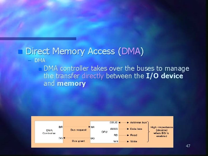
n Direct Memory Access (DMA) – DMA n DMA controller takes over the buses to manage the transfer directly between the I/O device and memory 47

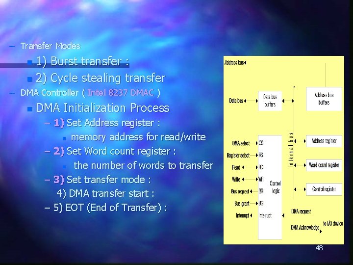
– Transfer Modes 1) Burst transfer : n 2) Cycle stealing transfer n – DMA Controller ( Intel 8237 DMAC ) n DMA Initialization Process – 1) Set Address register : n memory address for read/write – 2) Set Word count register : n the number of words to transfer – 3) Set transfer mode : 4) DMA transfer start : – 5) EOT (End of Transfer) : 48

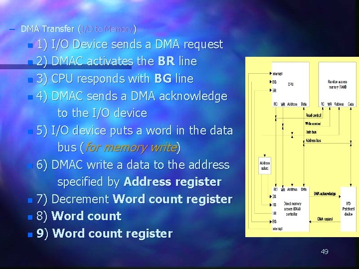
– DMA Transfer (I/O to Memory) 1) I/O Device sends a DMA request n 2) DMAC activates the BR line n 3) CPU responds with BG line n 4) DMAC sends a DMA acknowledge to the I/O device n 5) I/O device puts a word in the data bus (for memory write) n 6) DMAC write a data to the address specified by Address register n 7) Decrement Word count register n 8) Word count n 9) Word count register n 49

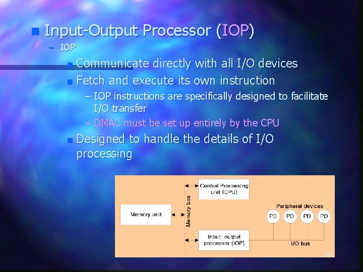
n Input-Output Processor (IOP) – IOP Communicate directly with all I/O devices n Fetch and execute its own instruction n – IOP instructions are specifically designed to facilitate I/O transfer – DMAC must be set up entirely by the CPU n Designed to handle the details of I/O processing 50

– CPU - IOP Communication n Memory units acts as a message center : – each processor leaves information for the other 51

Input/output Devices Input/output devices are required for users to communicate with the computer. n In simple terms, input devices bring information INTO the computer and output devices bring information OUT of a computer system. These input/output devices are also known as peripherals. n 52

Input Devices are: Keyboard n Mouse n Joystick n Scanner n Light Pen n Touch Screen n 53

Output devices are: Printers n Plotters n Monitor n LCD n 54

Intel 8086/8088 Microprocessors n Intel 8086 and 8088 Microprocessors are the basis of all IBM-PC compatible computers (8086 introduced in 1978, first IBM-PC released in 1981) All Intel, AMD and other advanced microprocessors are based on and are compatible with the original 8086/8 n At Power Up and Reset time, Pentiums, Athlons etc all look like 8086 processors n 55

Intel 8086/8088 Microprocessors n Intel 8086 is a 16 b microprocessor: – 16 b data registers, 16 b ALU n Width of external data bus: – 8086: 16 b – 8088: 8 b n n Width of external address bus: 16 b+4 b=20 b Some techniques to optimise the CPU performance when it’s executing programs Segment: Offset memory model Little-Endian Data Format 56

8086/8088 n n Original IBM PC used 8088 microprocessor 8088 is similar to the 8086, but it has an external 8 b data bus & only 4 B-deep queue – For cost reduction reasons n n n We can consider 8086 and 8088 together PC clones often used 8086 for better performance 8 -bit bus reduces performance, but meant cheaper computers 57

8086/8088 Functional Units 58

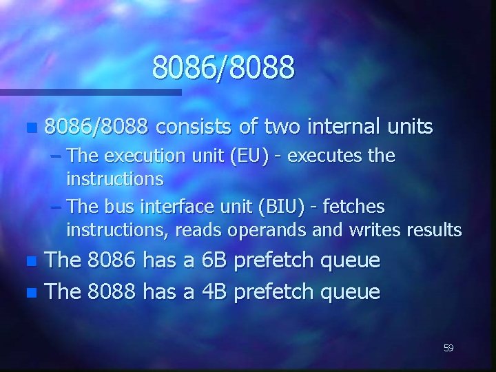
8086/8088 n 8086/8088 consists of two internal units – The execution unit (EU) - executes the instructions – The bus interface unit (BIU) - fetches instructions, reads operands and writes results The 8086 has a 6 B prefetch queue n The 8088 has a 4 B prefetch queue n 59

8086/8088 Internal Organisation 60

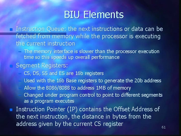
BIU Elements n Instruction Queue: the next instructions or data can be fetched from memory while the processor is executing the current instruction – The memory interface is slower than the processor execution time so this speeds up overall performance n Segment Registers: – – n CS, DS, SS and ES are 16 b registers Used with the 16 b Base registers to generate the 20 b address Allow the 8086/8088 to address 1 MB of memory Changed under program control to point to different segments as a program executes Instruction Pointer (IP) contains the Offset Address of the next instruction, the distance in bytes from the address given by the current CS register 61

8086/8088 20 -bit Addresses 62

BIU Elements n Instruction Queue: the next instructions or data can be fetched from memory while the processor is executing the current instruction – The memory interface is slower than the processor execution time so this speeds up overall performance n Segment Registers: – – n CS, DS, SS and ES are 16 b registers Used with the 16 b Base registers to generate the 20 b address Allow the 8086/8088 to address 1 MB of memory Changed under program control to point to different segments as a program executes Instruction Pointer (IP) contains the Offset Address of the next instruction, the distance in bytes from the address given by the current CS register 63

64

8086/8088 Summary First Generation (introduced June 1978) n One of the first 16 b processors on the market n 16 b internal registers n 16/8 b external data bus n 20 b address bus (1 MB addressable) n Used in 1 st generation IBM PCs (1981) n 65

n Thanks 66