Computer Architecture Prof Dr Nizamettin AYDIN naydinyildiz edu


- Slides: 34

Computer Architecture Prof. Dr. Nizamettin AYDIN naydin@yildiz. edu. tr nizamettinaydin@gmail. com http: //www. yildiz. edu. tr/~naydin 1

Internal Memory 2

Outline • Semiconductor main memory • Random Access Memory – Dynamic RAM – Static RAM • • Read Only Memory Organisation Error Correction Advanced DRAM Organization 3

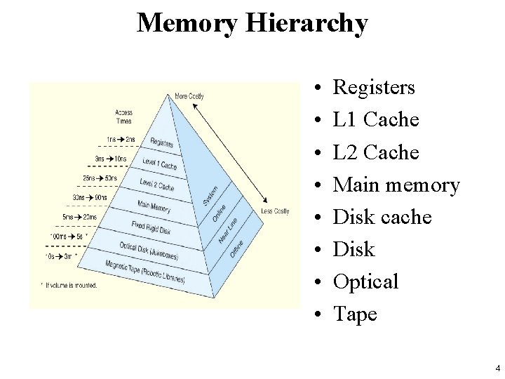
Memory Hierarchy • • Registers L 1 Cache L 2 Cache Main memory Disk cache Disk Optical Tape 4

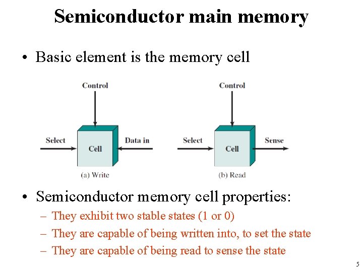
Semiconductor main memory • Basic element is the memory cell • Semiconductor memory cell properties: – They exhibit two stable states (1 or 0) – They are capable of being written into, to set the state – They are capable of being read to sense the state 5

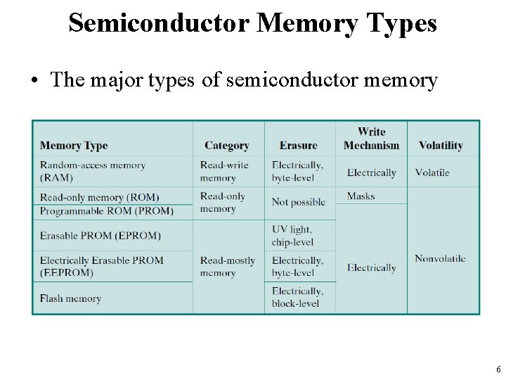
Semiconductor Memory Types • The major types of semiconductor memory 6

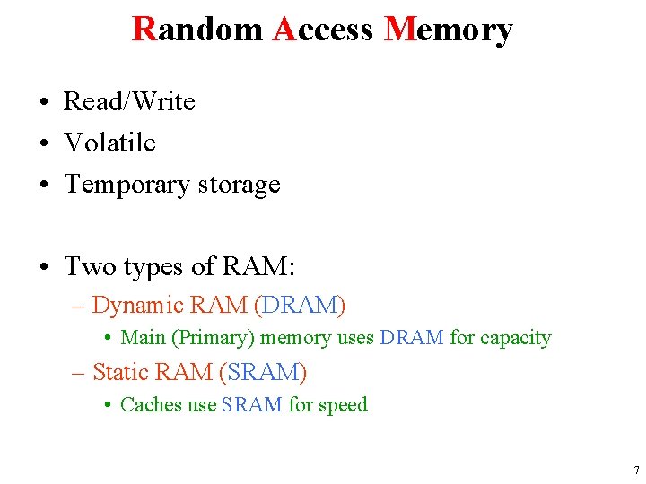
Random Access Memory • Read/Write • Volatile • Temporary storage • Two types of RAM: – Dynamic RAM (DRAM) • Main (Primary) memory uses DRAM for capacity – Static RAM (SRAM) • Caches use SRAM for speed 7

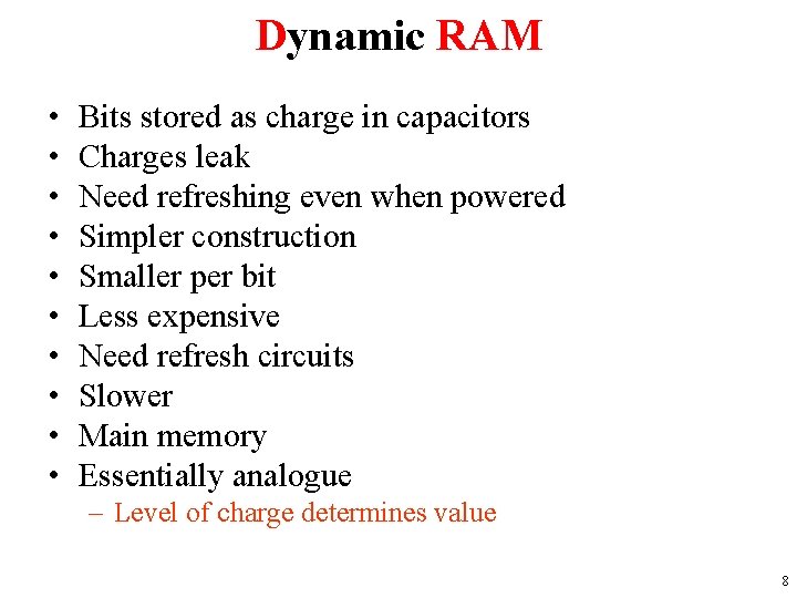
Dynamic RAM • • • Bits stored as charge in capacitors Charges leak Need refreshing even when powered Simpler construction Smaller per bit Less expensive Need refresh circuits Slower Main memory Essentially analogue – Level of charge determines value 8

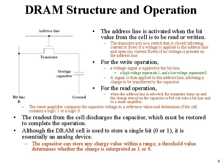
DRAM Structure and Operation • The address line is activated when the bit value from the cell is to be read or written. – The transistor acts as a switch that is closed (allowing current to flow) if a voltage is applied to the address line and open (no current flows) if no voltage is present on the address line. • For the write operation, – a voltage signal is applied to the bit line; • – a high voltage represents 1, and a low voltage represents 0. A signal is then applied to the address line, allowing a charge to be transferred to the capacitor. • For the read operation, – – when the address line is selected, the transistor turns on and the charge stored on the capacitor is fed out onto a bit line and to a sense amplifier. The sense amplifier compares the capacitor voltage to a reference value and determines if the cell contains a logic 1 or a logic 0. • The readout from the cell discharges the capacitor, which must be restored to complete the operation. • Although the DRAM cell is used to store a single bit (0 or 1), it is essentially an analog device. – The capacitor can store any charge value within a range; a threshold value determines whether the charge is interpreted as 1 or 0. 9

Static RAM • • • Bits stored as on/off switches No charges to leak No refreshing needed when powered More complex construction Larger per bit More expensive Does not need refresh circuits Faster Cache Digital – Uses flip-flops 10

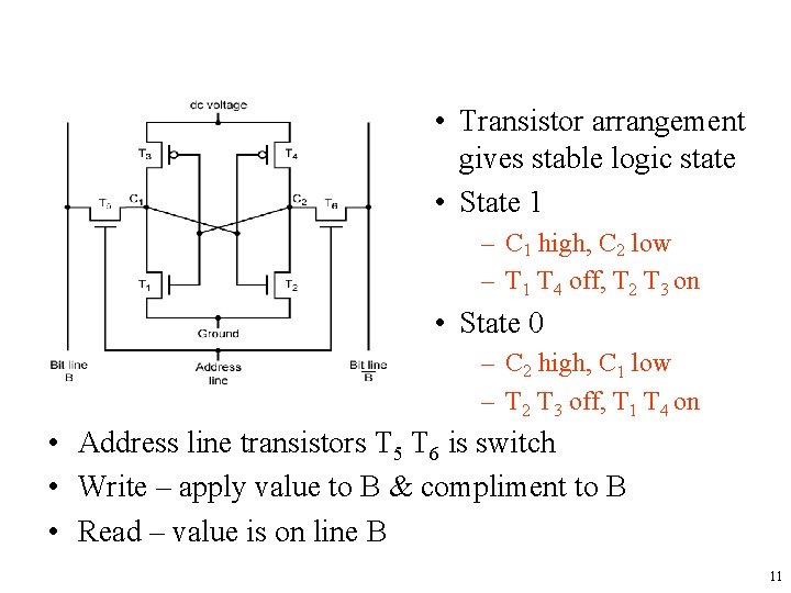
• Transistor arrangement gives stable logic state • State 1 – C 1 high, C 2 low – T 1 T 4 off, T 2 T 3 on • State 0 – C 2 high, C 1 low – T 2 T 3 off, T 1 T 4 on • Address line transistors T 5 T 6 is switch • Write – apply value to B & compliment to B • Read – value is on line B 11

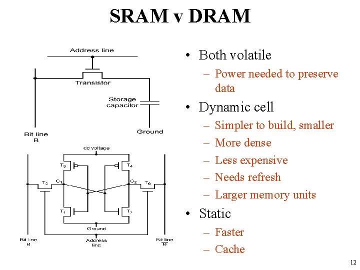
SRAM v DRAM • Both volatile – Power needed to preserve data • Dynamic cell – – – Simpler to build, smaller More dense Less expensive Needs refresh Larger memory units • Static – Faster – Cache 12

Read Only Memory • Permanent storage – Nonvolatile • Used in: – Microprogramming – Library subroutines – Systems programs (BIOS) – Function tables 13

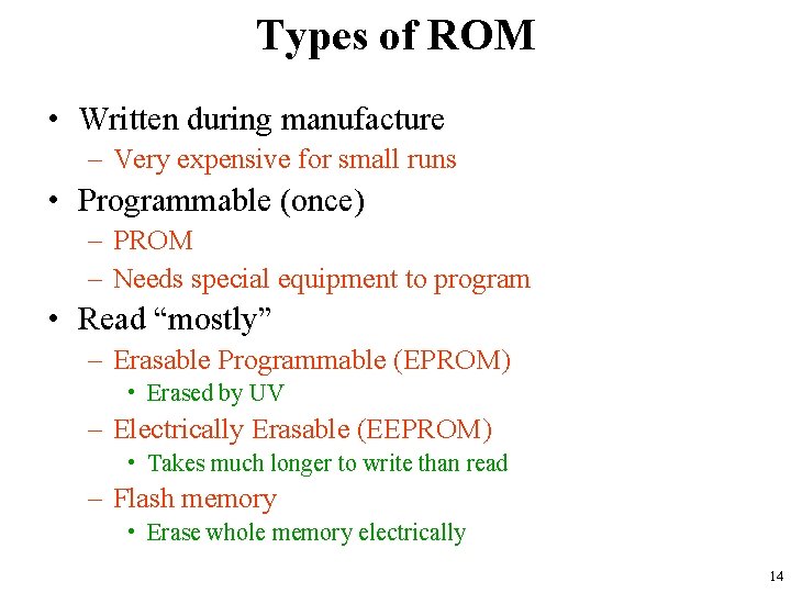
Types of ROM • Written during manufacture – Very expensive for small runs • Programmable (once) – PROM – Needs special equipment to program • Read “mostly” – Erasable Programmable (EPROM) • Erased by UV – Electrically Erasable (EEPROM) • Takes much longer to write than read – Flash memory • Erase whole memory electrically 14

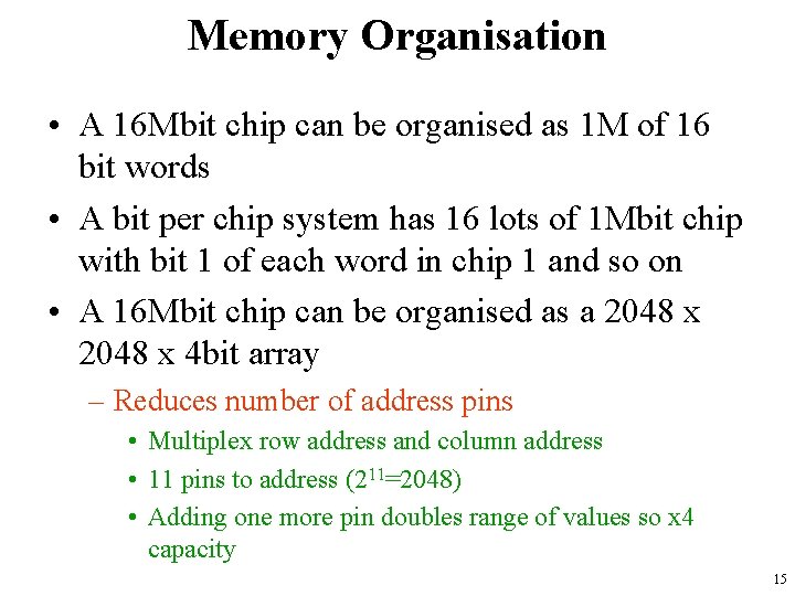
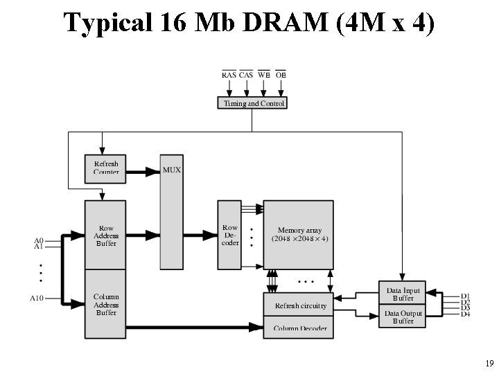
Memory Organisation • A 16 Mbit chip can be organised as 1 M of 16 bit words • A bit per chip system has 16 lots of 1 Mbit chip with bit 1 of each word in chip 1 and so on • A 16 Mbit chip can be organised as a 2048 x 4 bit array – Reduces number of address pins • Multiplex row address and column address • 11 pins to address (211=2048) • Adding one more pin doubles range of values so x 4 capacity 15

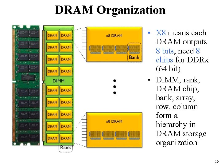
DRAM Organization • X 8 means each DRAM outputs 8 bits, need 8 chips for DDRx (64 bit) • DIMM, rank, DRAM chip, bank, array, row, column form a hierarchy in DRAM storage organization 16

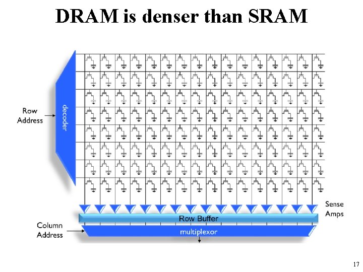
DRAM is denser than SRAM 17

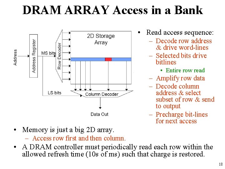
DRAM ARRAY Access in a Bank • Read access sequence: – Decode row address & drive word-lines – Selected bits drive bitlines • Entire row read – Amplify row data – Decode column address & select subset of row & send to output – Precharge bit-lines for next access • Memory is just a big 2 D array. – Access row first and then column. • A DRAM controller must periodically read each row within the allowed refresh time (10 s of ms) such that charge is restored. 18

Typical 16 Mb DRAM (4 M x 4) 19

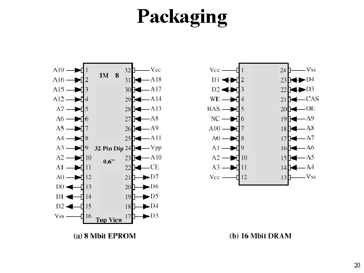
Packaging 20

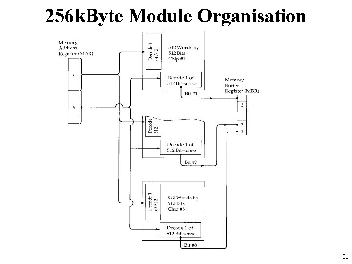
256 k. Byte Module Organisation 21

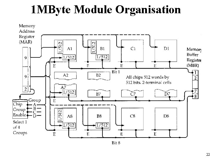
1 MByte Module Organisation 22

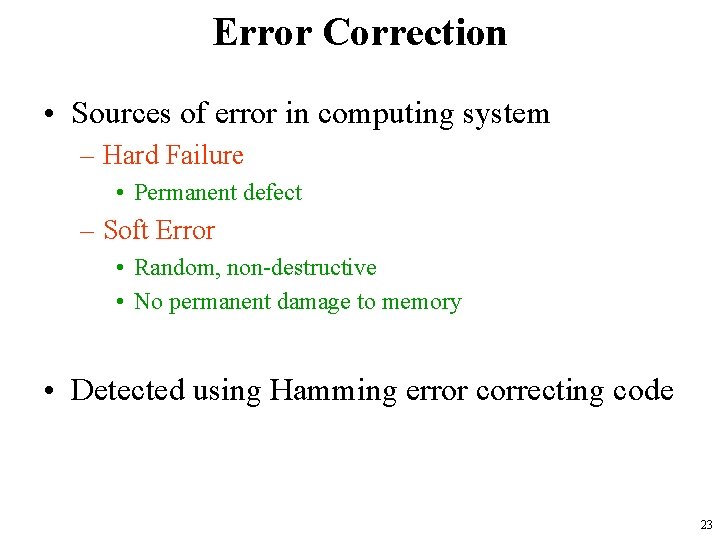
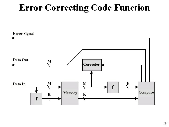
Error Correction • Sources of error in computing system – Hard Failure • Permanent defect – Soft Error • Random, non-destructive • No permanent damage to memory • Detected using Hamming error correcting code 23

Error Correcting Code Function 24

Advanced DRAM Organization • Basic DRAM same since first RAM chips • Enhanced DRAM – Contains small SRAM as well – SRAM holds last line read • Cache DRAM – Larger SRAM component – Use as cache or serial buffer 25

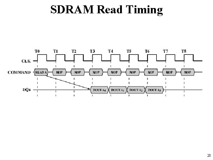
Synchronous DRAM • Access is synchronized with an external clock • Address is presented to RAM • RAM finds data (CPU waits in conventional DRAM) • Since SDRAM moves data in time with system clock, CPU knows when data will be ready • CPU does not have to wait, it can do something else • Burst mode allows SDRAM to set up stream of data and fire it out in block 26

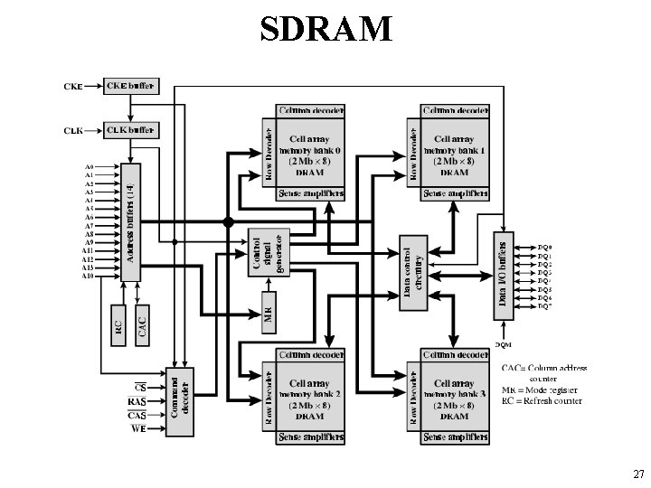
SDRAM 27

SDRAM Read Timing 28

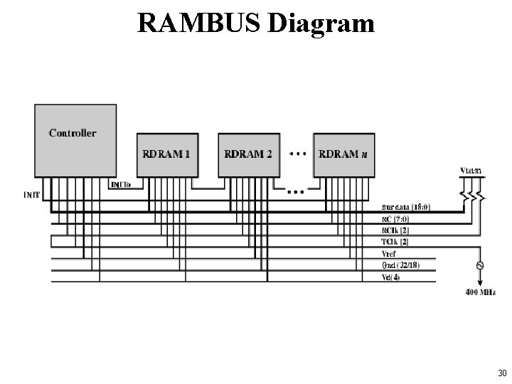
RAMBUS • • • Adopted by Intel for Pentium & Itanium Main competitor to SDRAM Vertical package – all pins on one side Data exchange over 28 wires < cm long Bus addresses up to 320 RDRAM chips at 1. 6 Gbps • Asynchronous block protocol – 480 ns access time – Then 1. 6 Gbps 29

RAMBUS Diagram 30

DDR SDRAM • SDRAM can only send data once per clock • Double-Data-Rate SDRAM can send data twice per clock cycle – Rising edge and falling edge 31

Cache DRAM • Mitsubishi • Integrates small SRAM cache (16 kb) onto generic DRAM chip • Used as true cache – 64 -bit lines – Effective for ordinary random access • To support serial access of block of data – E. g. refresh bit-mapped screen • CDRAM can prefetch data from DRAM into SRAM buffer • Subsequent accesses solely to SRAM 32

Memory Technology Cost • Bigger is slower – – SRAM, 512 Bytes, sub-nanosec SRAM, KByte~MByte, ~nanosec DRAM, Gigabyte, ~50 nanosec Hard Disk, Terabyte, ~10 millisec • Faster is more expensive (dollars and chip area) – – SRAM, < 10$ per Megabyte DRAM, < 1$ per Megabyte Hard Disk < 1$ per Gigabyte These sample values scale with time • Other technologies have their place as well – Flash memory, Phase-change memory (not mature yet) 33

34