Computer Architecture Prof Dr Nizamettin AYDIN naydinyildiz edu

- Slides: 172

Computer Architecture Prof. Dr. Nizamettin AYDIN naydin@yildiz. edu. tr http: //www. yildiz. edu. tr/~naydin 1

Information Systems: Fundamentals 2

Informatics • The term informatics broadly describes the study and practice of – creating, – storing, – finding, – manipulating – sharing information. 3

Informatics - Etymology • In 1956 the German computer scientist Karl Steinbuch coined the word Informatik • [Informatik: Automatische Informationsverarbeitung ("Informatics: Automatic Information Processing")] • The French term informatique was coined in 1962 by Philippe Dreyfus • [Dreyfus, Phillipe. L’informatique. Gestion, Paris, June 1962, pp. 240– 41] • The term was coined as a combination of information and automatic to describe the science of automating information interactions 4

Informatics - Etymology • The morphology—informat-ion + -ics—uses • the accepted form for names of sciences, – as conics, linguistics, optics, • or matters of practice, – as economics, politics, tactics • linguistically, the meaning extends easily – to encompass both • the science of information • the practice of information processing. 5

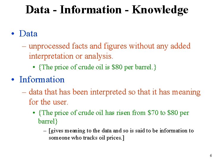
Data - Information - Knowledge • Data – unprocessed facts and figures without any added interpretation or analysis. • {The price of crude oil is $80 per barrel. } • Information – data that has been interpreted so that it has meaning for the user. • {The price of crude oil has risen from $70 to $80 per barrel} – [gives meaning to the data and so is said to be information to someone who tracks oil prices. ] 6

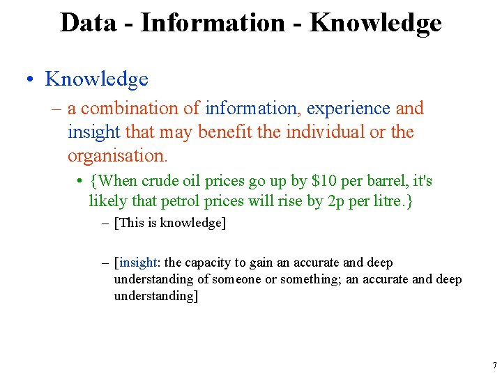
Data - Information - Knowledge • Knowledge – a combination of information, experience and insight that may benefit the individual or the organisation. • {When crude oil prices go up by $10 per barrel, it's likely that petrol prices will rise by 2 p per litre. } – [This is knowledge] – [insight: the capacity to gain an accurate and deep understanding of someone or something; an accurate and deep understanding] 7

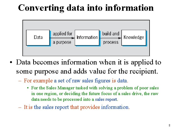
Converting data into information • Data becomes information when it is applied to some purpose and adds value for the recipient. – For example a set of raw sales figures is data. • For the Sales Manager tasked with solving a problem of poor sales in one region, or deciding the future focus of a sales drive, the raw data needs to be processed into a sales report. – It is the sales report that provides information. 8

Converting data into information • Collecting data is expensive – you need to be very clear about why you need it and how you plan to use it. – One of the main reasons that organisations collect data is to monitor and improve performance. • if you are to have the information you need for control and performance improvement, you need to: – collect data on the indicators that really do affect performance – collect data reliably and regularly – be able to convert data into the information you need. 9

Converting data into information • To be useful, data must satisfy a number of conditions. It must be: – relevant to the specific purpose – complete – accurate – timely • data that arrives after you have made your decision is of no value 10

Converting data into information – in the right format • information can only be analysed using a spreadsheet if all the data can be entered into the computer system – available at a suitable price • the benefits of the data must merit the cost of collecting or buying it. • The same criteria apply to information. – It is important • to get the right information • to get the information right 11

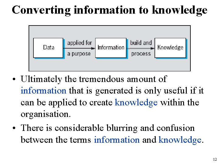
Converting information to knowledge • Ultimately the tremendous amount of information that is generated is only useful if it can be applied to create knowledge within the organisation. • There is considerable blurring and confusion between the terms information and knowledge. 12

Converting information to knowledge • think of knowledge as being of two types: – Formal, explicit or generally available knowledge. • This is knowledge that has been captured and used to develop policies and operating procedures for example. – Instinctive, subconscious, tacit or hidden knowledge. • Within the organisation there are certain people who hold specific knowledge or have the 'know how' – {"I did something very similar to that last year and this happened…. . "} 13

Converting information to knowledge • Clearly, both types of knowledge are essential for the organisation. • Information on its own will not create a knowledge-based organisation – but it is a key building block. • The right information fuels the development of intellectual capital – which in turns drives innovation and performance improvement. 14

Definition(s) of system • A system can be broadly defined as an integrated set of elements that accomplish a defined objective. • People from different engineering disciplines have different perspectives of what a "system" is. • For example, – software engineers often refer to an integrated set of computer programs as a "system" – electrical engineers might refer to complex integrated circuits or an integrated set of electrical units as a "system" • As can be seen, "system" depends on one’s perspective, and the “integrated set of elements that accomplish a defined objective” is an appropriate definition. 15

Definition(s) of system • A system is an assembly of parts where: – The parts or components are connected together in an organized way. – The parts or components are affected by being in the system (and are changed by leaving it). – The assembly does something. – The assembly has been identified by a person as being of special interest. • Any arrangement which involves the handling, processing or manipulation of resources of whatever type can be represented as a system. • Some definitions on online dictionaries – http: //en. wikipedia. org/wiki/System – http: //dictionary. reference. com/browse/systems – http: //www. businessdictionary. com/definition/system. html 16

Definition(s) of system • A system is defined as multiple parts working together for a common purpose or goal. • Systems can be large and complex – such as the air traffic control system or our global telecommunication network. • Small devices can also be considered as systems – such as a pocket calculator, alarm clock, or 10 speed bicycle. 17

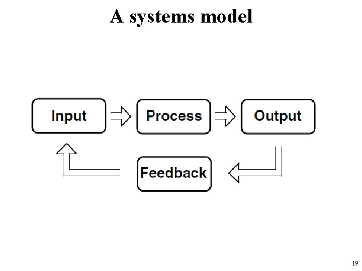
Definition(s) of system • Systems have inputs, processes, and outputs. • When feedback (direct or indirect) is involved, that component is also important to the operation of the system. • To explain all this, systems are usually explained using a model. • A model helps to illustrate the major elements and their relationship, as illustrated in the next slide 18

A systems model 19

Information Systems • The ways that organizations – Store – Move – Organize – Process their information 20

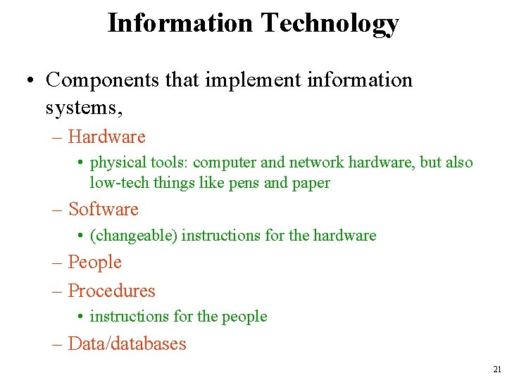
Information Technology • Components that implement information systems, – Hardware • physical tools: computer and network hardware, but also low-tech things like pens and paper – Software • (changeable) instructions for the hardware – People – Procedures • instructions for the people – Data/databases 21

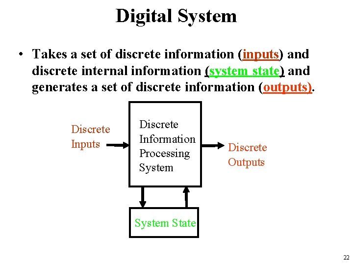
Digital System • Takes a set of discrete information (inputs) and discrete internal information (system state) and generates a set of discrete information (outputs). Discrete Inputs Discrete Information Processing System Discrete Outputs System State 22

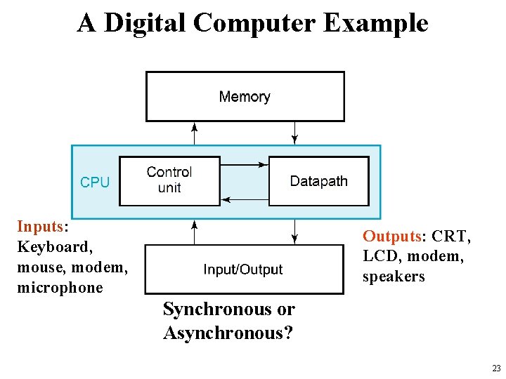
A Digital Computer Example Inputs: Keyboard, mouse, modem, microphone Outputs: CRT, LCD, modem, speakers Synchronous or Asynchronous? 23

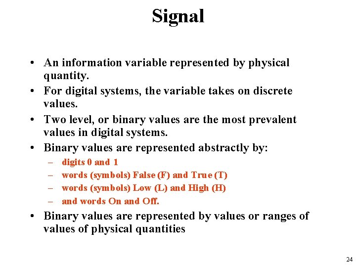
Signal • An information variable represented by physical quantity. • For digital systems, the variable takes on discrete values. • Two level, or binary values are the most prevalent values in digital systems. • Binary values are represented abstractly by: – – digits 0 and 1 words (symbols) False (F) and True (T) words (symbols) Low (L) and High (H) and words On and Off. • Binary values are represented by values or ranges of values of physical quantities 24

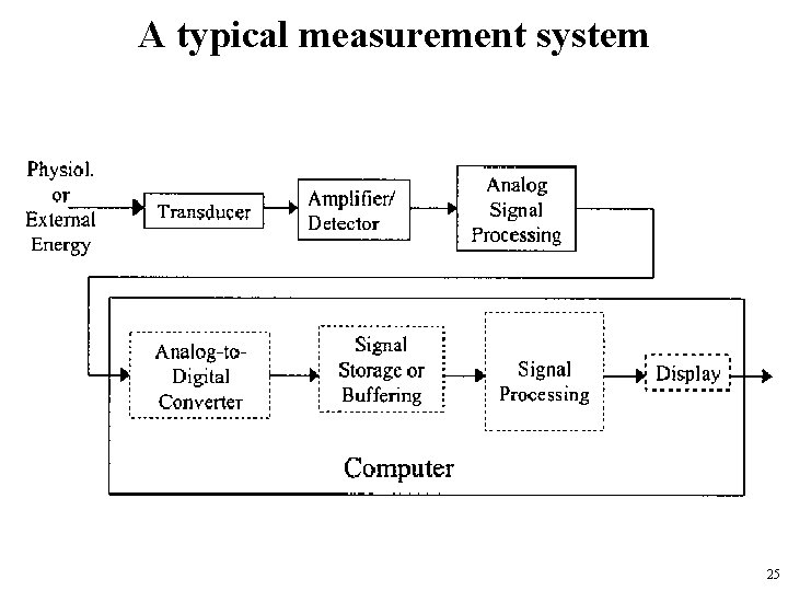
A typical measurement system 25

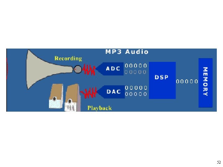
Transducers • A “transducer” is a device that converts energy from one form to another. • In signal processing applications, the purpose of energy conversion is to transfer information, not to transform energy. • In physiological measurement systems, transducers may be – input transducers (or sensors) • they convert a non-electrical energy into an electrical signal. • for example, a microphone. – output transducers (or actuators) • they convert an electrical signal into a non-electrical energy. • For example, a speaker. 26

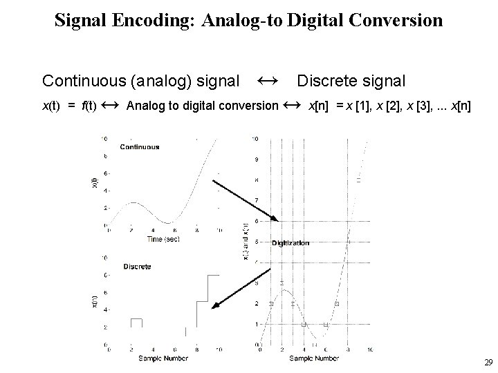
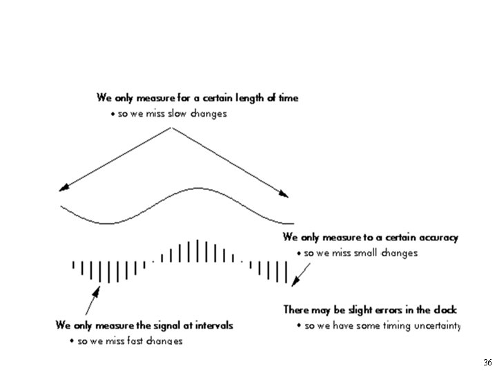
Analogue signal • The analogue signal – a continuous variable defined with infinite precision is converted to a discrete sequence of measured values which are represented digitally • Information is lost in converting from analogue to digital, due to: – inaccuracies in the measurement – uncertainty in timing – limits on the duration of the measurement • These effects are called quantisation errors 27

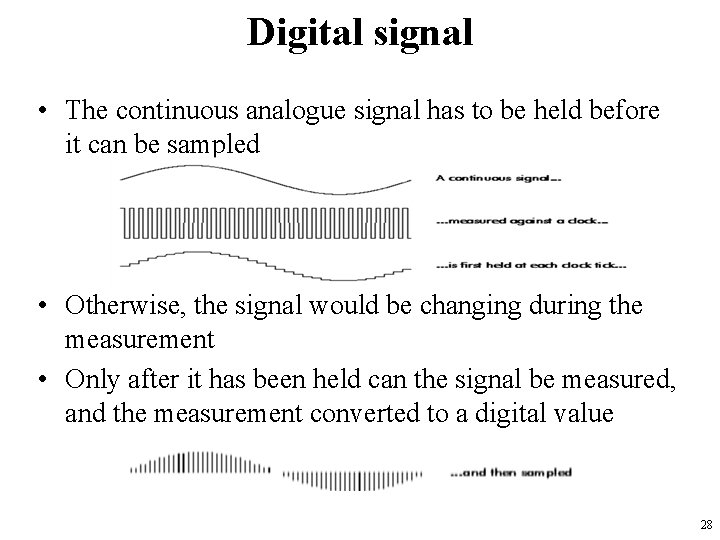
Digital signal • The continuous analogue signal has to be held before it can be sampled • Otherwise, the signal would be changing during the measurement • Only after it has been held can the signal be measured, and the measurement converted to a digital value 28

Signal Encoding: Analog-to Digital Conversion Continuous (analog) signal ↔ Discrete signal x(t) = f(t) ↔ Analog to digital conversion ↔ x[n] = x [1], x [2], x [3], . . . x[n] 29

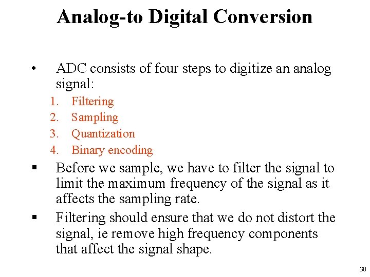
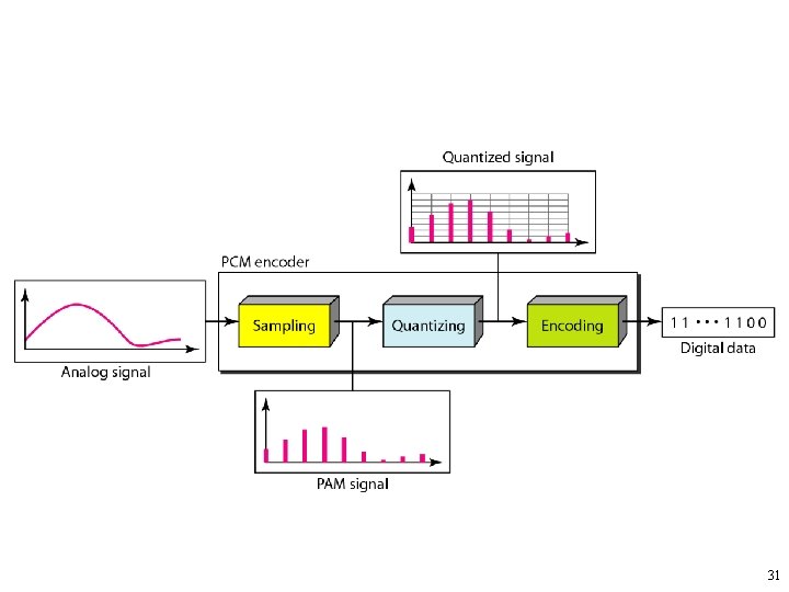
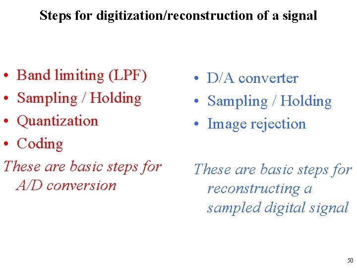
Analog-to Digital Conversion • ADC consists of four steps to digitize an analog signal: 1. 2. 3. 4. § § Filtering Sampling Quantization Binary encoding Before we sample, we have to filter the signal to limit the maximum frequency of the signal as it affects the sampling rate. Filtering should ensure that we do not distort the signal, ie remove high frequency components that affect the signal shape. 30

31

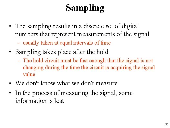
Sampling • The sampling results in a discrete set of digital numbers that represent measurements of the signal – usually taken at equal intervals of time • Sampling takes place after the hold – The hold circuit must be fast enough that the signal is not changing during the time the circuit is acquiring the signal value • We don't know what we don't measure • In the process of measuring the signal, some information is lost 32

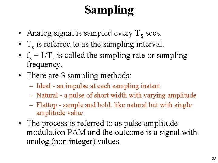
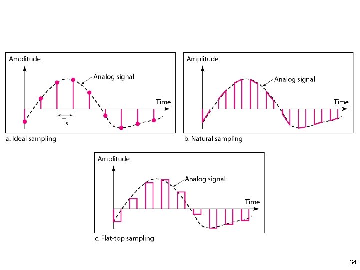
Sampling • Analog signal is sampled every TS secs. • Ts is referred to as the sampling interval. • fs = 1/Ts is called the sampling rate or sampling frequency. • There are 3 sampling methods: – Ideal - an impulse at each sampling instant – Natural - a pulse of short width with varying amplitude – Flattop - sample and hold, like natural but with single amplitude value • The process is referred to as pulse amplitude modulation PAM and the outcome is a signal with analog (non integer) values 33

34

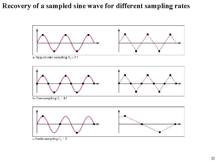
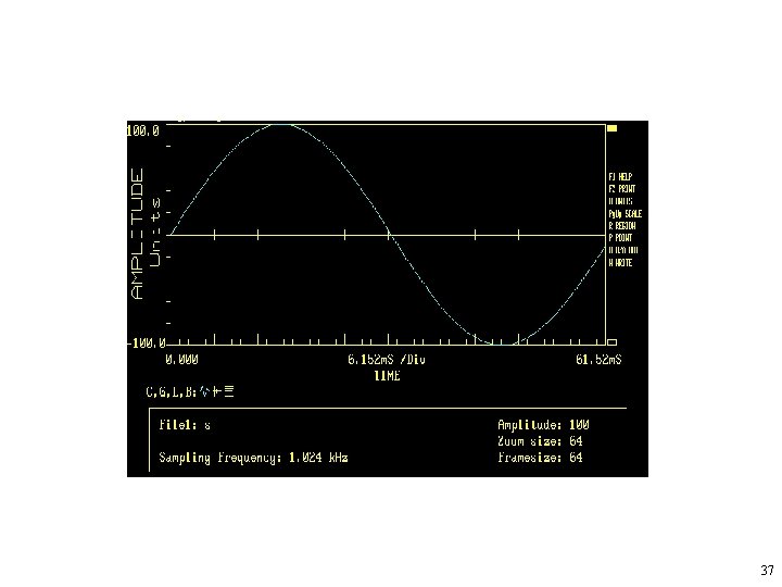
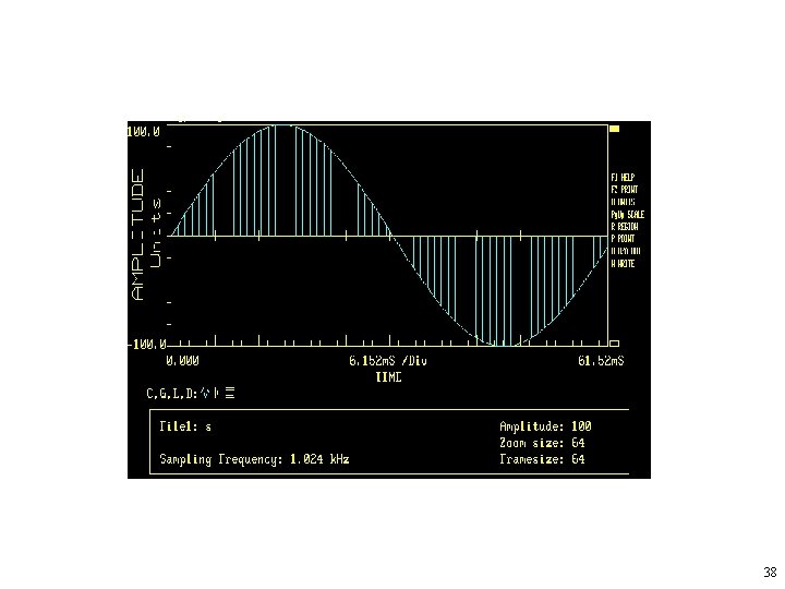
Recovery of a sampled sine wave for different sampling rates 35

36

37

38

39

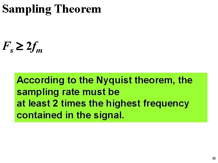
Sampling Theorem Fs 2 fm According to the Nyquist theorem, the sampling rate must be at least 2 times the highest frequency contained in the signal. 40

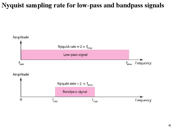
Nyquist sampling rate for low-pass and bandpass signals 41

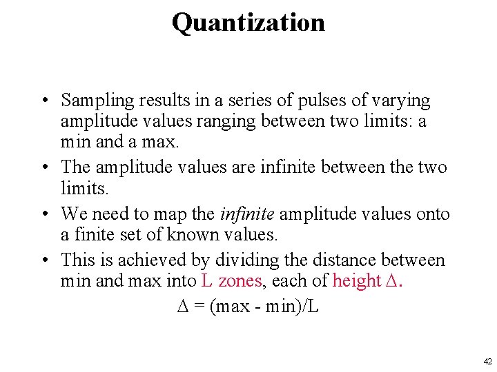
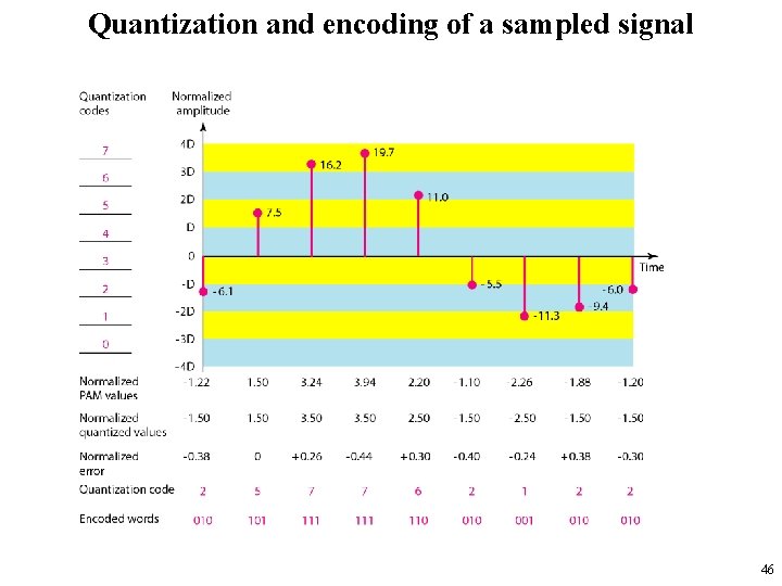
Quantization • Sampling results in a series of pulses of varying amplitude values ranging between two limits: a min and a max. • The amplitude values are infinite between the two limits. • We need to map the infinite amplitude values onto a finite set of known values. • This is achieved by dividing the distance between min and max into L zones, each of height = (max - min)/L 42

Quantization Levels • The midpoint of each zone is assigned a value from 0 to L-1 (resulting in L values) • Each sample falling in a zone is then approximated to the value of the midpoint. 43

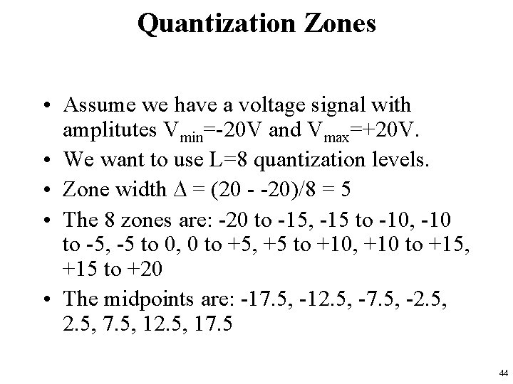
Quantization Zones • Assume we have a voltage signal with amplitutes Vmin=-20 V and Vmax=+20 V. • We want to use L=8 quantization levels. • Zone width = (20 - -20)/8 = 5 • The 8 zones are: -20 to -15, -15 to -10, -10 to -5, -5 to 0, 0 to +5, +5 to +10, +10 to +15, +15 to +20 • The midpoints are: -17. 5, -12. 5, -7. 5, -2. 5, 7. 5, 12. 5, 17. 5 44

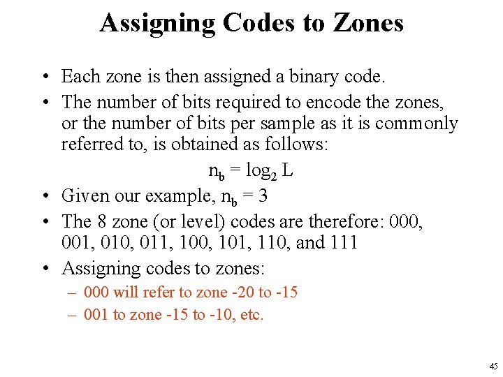
Assigning Codes to Zones • Each zone is then assigned a binary code. • The number of bits required to encode the zones, or the number of bits per sample as it is commonly referred to, is obtained as follows: nb = log 2 L • Given our example, nb = 3 • The 8 zone (or level) codes are therefore: 000, 001, 010, 011, 100, 101, 110, and 111 • Assigning codes to zones: – 000 will refer to zone -20 to -15 – 001 to zone -15 to -10, etc. 45

Quantization and encoding of a sampled signal 46

Quantization Error • When a signal is quantized, we introduce an error – the coded signal is an approximation of the actual amplitude value. • The difference between actual and coded value (midpoint) is referred to as the quantization error. • The more zones, the smaller – which results in smaller errors. • BUT, the more zones the more bits required to encode the samples – higher bit rate 47

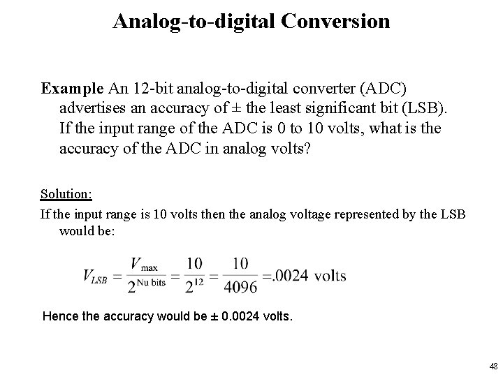
Analog-to-digital Conversion Example An 12 -bit analog-to-digital converter (ADC) advertises an accuracy of ± the least significant bit (LSB). If the input range of the ADC is 0 to 10 volts, what is the accuracy of the ADC in analog volts? Solution: If the input range is 10 volts then the analog voltage represented by the LSB would be: Hence the accuracy would be ± 0. 0024 volts. 48

Sampling related concepts • • Over/exact/under sampling Regular/irregular sampling Linear/Logarithmic sampling Aliasing Anti-aliasing filter Image Anti-image filter 49

Steps for digitization/reconstruction of a signal • Band limiting (LPF) • Sampling / Holding • Quantization • Coding These are basic steps for A/D conversion • D/A converter • Sampling / Holding • Image rejection These are basic steps for reconstructing a sampled digital signal 50

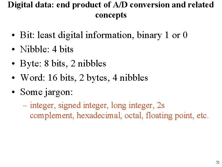
Digital data: end product of A/D conversion and related concepts • • • Bit: least digital information, binary 1 or 0 Nibble: 4 bits Byte: 8 bits, 2 nibbles Word: 16 bits, 2 bytes, 4 nibbles Some jargon: – integer, signed integer, long integer, 2 s complement, hexadecimal, octal, floating point, etc. 51

52

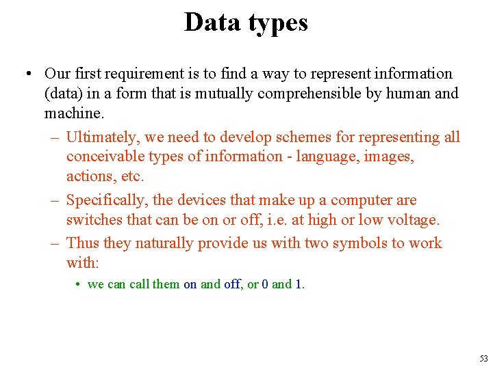
Data types • Our first requirement is to find a way to represent information (data) in a form that is mutually comprehensible by human and machine. – Ultimately, we need to develop schemes for representing all conceivable types of information - language, images, actions, etc. – Specifically, the devices that make up a computer are switches that can be on or off, i. e. at high or low voltage. – Thus they naturally provide us with two symbols to work with: • we can call them on and off, or 0 and 1. 53

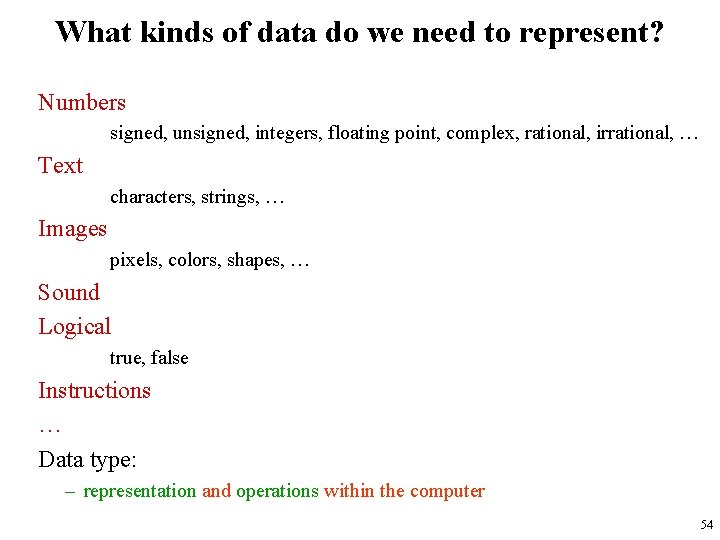
What kinds of data do we need to represent? Numbers signed, unsigned, integers, floating point, complex, rational, irrational, … Text characters, strings, … Images pixels, colors, shapes, … Sound Logical true, false Instructions … Data type: – representation and operations within the computer 54

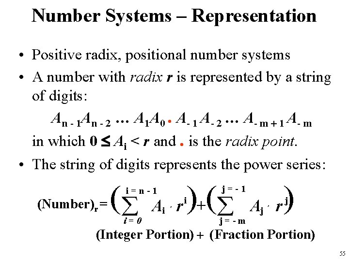
Number Systems – Representation • Positive radix, positional number systems • A number with radix r is represented by a string of digits: An - 1 An - 2 … A 1 A 0. A- 1 A- 2 … A- m + 1 A- m in which 0 £ Ai < r and. is the radix point. • The string of digits represents the power series: (å i=n-1 (Number)r = i=0 Ai r )+( å j=-1 i j=-m Aj r) j (Integer Portion) + (Fraction Portion) 55

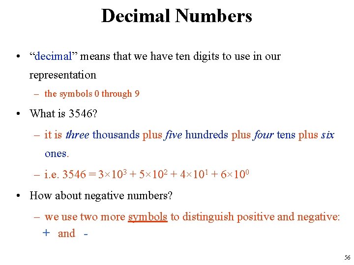
Decimal Numbers • “decimal” means that we have ten digits to use in our representation – the symbols 0 through 9 • What is 3546? – it is three thousands plus five hundreds plus four tens plus six ones. – i. e. 3546 = 3× 10³ + 5× 10² + 4× 101 + 6× 100 • How about negative numbers? – we use two more symbols to distinguish positive and negative: + and 56

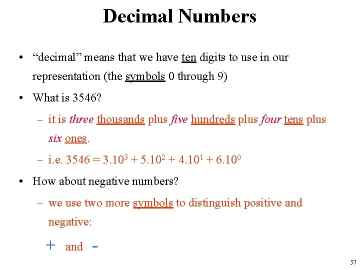
Decimal Numbers • “decimal” means that we have ten digits to use in our representation (the symbols 0 through 9) • What is 3546? – it is three thousands plus five hundreds plus four tens plus six ones. – i. e. 3546 = 3. 103 + 5. 102 + 4. 101 + 6. 100 • How about negative numbers? – we use two more symbols to distinguish positive and negative: + and 57

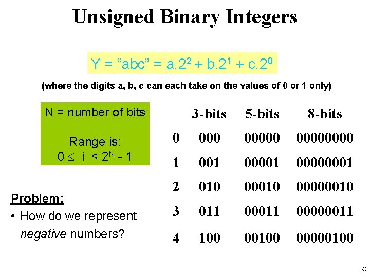
Unsigned Binary Integers Y = “abc” = a. 22 + b. 21 + c. 20 (where the digits a, b, c can each take on the values of 0 or 1 only) N = number of bits Range is: 0 i < 2 N - 1 Problem: • How do we represent negative numbers? 3 -bits 5 -bits 8 -bits 0 00000 1 00001 00000001 2 010 00000010 3 011 00000011 4 100 00000100 58

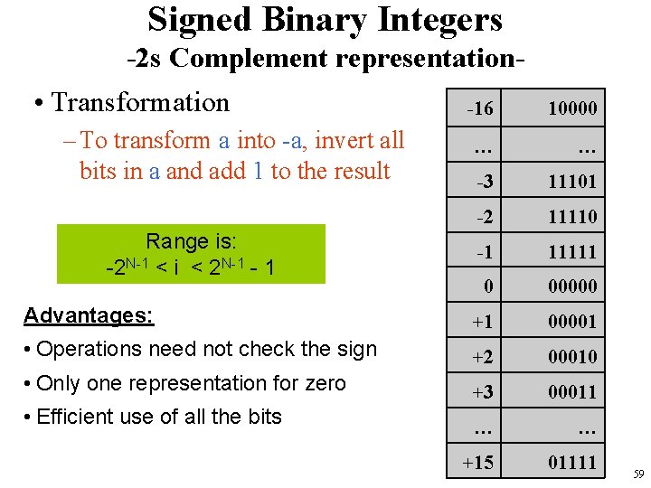
Signed Binary Integers -2 s Complement representation- • Transformation -16 10000 … … -3 11101 -2 11110 -1 11111 0 00000 Advantages: +1 00001 • Operations need not check the sign +2 00010 • Only one representation for zero +3 00011 • Efficient use of all the bits … … +15 01111 – To transform a into -a, invert all bits in a and add 1 to the result Range is: -2 N-1 < i < 2 N-1 - 1 59

Limitations of integer representations • Most numbers are not integer! – Even with integers, there are two other considerations: • Range: – The magnitude of the numbers we can represent is determined by how many bits we use: • e. g. with 32 bits the largest number we can represent is about +/- 2 billion, far too small for many purposes. • Precision: – The exactness with which we can specify a number: • e. g. a 32 bit number gives us 31 bits of precision, or roughly 9 figure precision in decimal repesentation. • We need another data type! 60

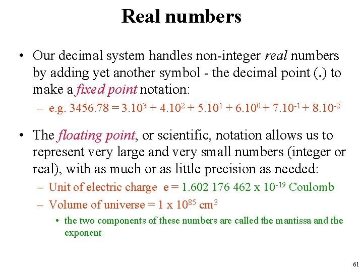
Real numbers • Our decimal system handles non-integer real numbers by adding yet another symbol - the decimal point (. ) to make a fixed point notation: – e. g. 3456. 78 = 3. 103 + 4. 102 + 5. 101 + 6. 100 + 7. 10 -1 + 8. 10 -2 • The floating point, or scientific, notation allows us to represent very large and very small numbers (integer or real), with as much or as little precision as needed: – Unit of electric charge e = 1. 602 176 462 x 10 -19 Coulomb – Volume of universe = 1 x 1085 cm 3 • the two components of these numbers are called the mantissa and the exponent 61

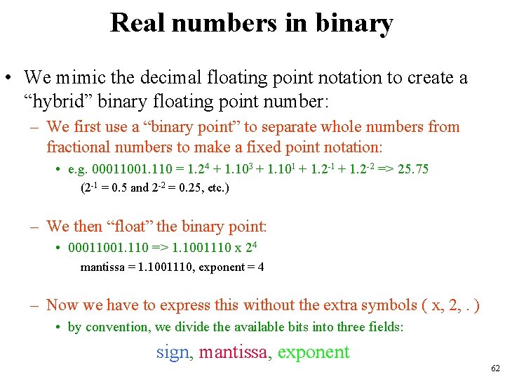
Real numbers in binary • We mimic the decimal floating point notation to create a “hybrid” binary floating point number: – We first use a “binary point” to separate whole numbers from fractional numbers to make a fixed point notation: • e. g. 00011001. 110 = 1. 24 + 1. 103 + 1. 101 + 1. 2 -2 => 25. 75 (2 -1 = 0. 5 and 2 -2 = 0. 25, etc. ) – We then “float” the binary point: • 00011001. 110 => 1. 1001110 x 24 mantissa = 1. 1001110, exponent = 4 – Now we have to express this without the extra symbols ( x, 2, . ) • by convention, we divide the available bits into three fields: sign, mantissa, exponent 62

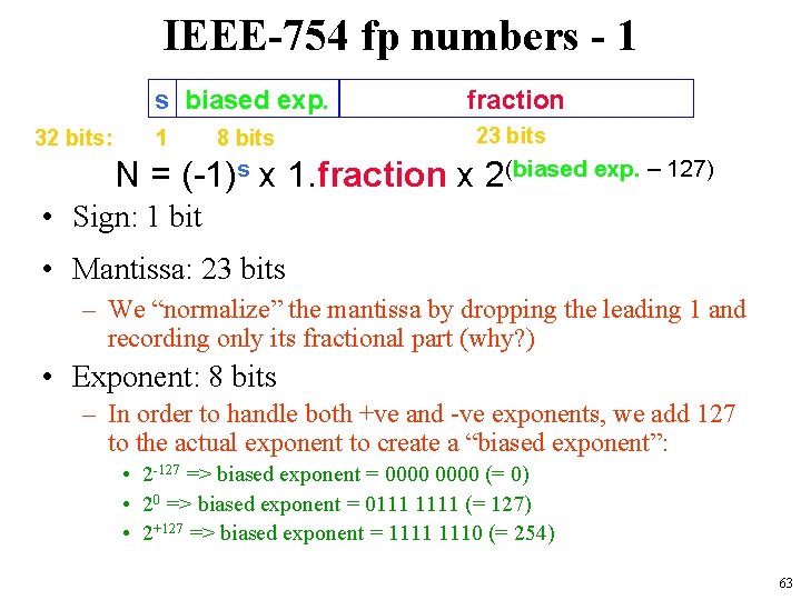
IEEE-754 fp numbers - 1 s biased exp. 32 bits: 1 8 bits fraction 23 bits N = (-1)s x 1. fraction x 2(biased exp. – 127) • Sign: 1 bit • Mantissa: 23 bits – We “normalize” the mantissa by dropping the leading 1 and recording only its fractional part (why? ) • Exponent: 8 bits – In order to handle both +ve and -ve exponents, we add 127 to the actual exponent to create a “biased exponent”: • 2 -127 => biased exponent = 0000 (= 0) • 20 => biased exponent = 0111 1111 (= 127) • 2+127 => biased exponent = 1111 1110 (= 254) 63

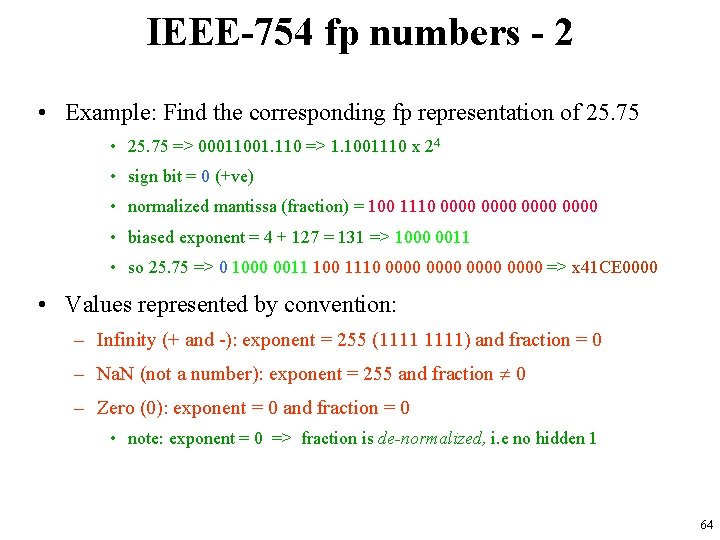
IEEE-754 fp numbers - 2 • Example: Find the corresponding fp representation of 25. 75 • 25. 75 => 00011001. 110 => 1. 1001110 x 24 • sign bit = 0 (+ve) • normalized mantissa (fraction) = 100 1110 0000 • biased exponent = 4 + 127 = 131 => 1000 0011 • so 25. 75 => 0 1000 0011 100 1110 0000 => x 41 CE 0000 • Values represented by convention: – Infinity (+ and -): exponent = 255 (1111) and fraction = 0 – Na. N (not a number): exponent = 255 and fraction 0 – Zero (0): exponent = 0 and fraction = 0 • note: exponent = 0 => fraction is de-normalized, i. e no hidden 1 64

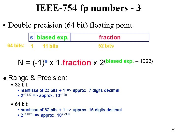
IEEE-754 fp numbers - 3 • Double precision (64 bit) floating point 64 bits: s biased exp. fraction 1 52 bits 11 bits N = (-1)s x 1. fraction x 2(biased exp. – 1023) l Range & Precision: w 32 bit: § mantissa of 23 bits + 1 => approx. 7 digits decimal § 2+/-127 => approx. 10+/-38 w 64 bit: § mantissa of 52 bits + 1 => approx. 15 digits decimal § 2+/-1023 => approx. 10+/-306 65

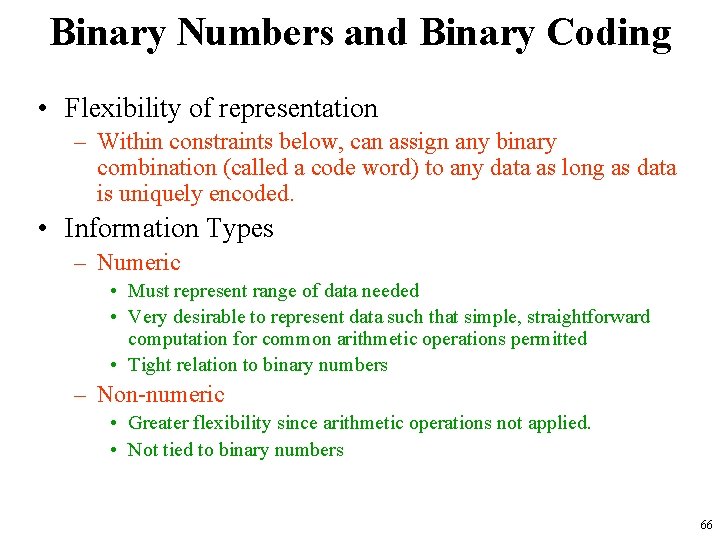
Binary Numbers and Binary Coding • Flexibility of representation – Within constraints below, can assign any binary combination (called a code word) to any data as long as data is uniquely encoded. • Information Types – Numeric • Must represent range of data needed • Very desirable to represent data such that simple, straightforward computation for common arithmetic operations permitted • Tight relation to binary numbers – Non-numeric • Greater flexibility since arithmetic operations not applied. • Not tied to binary numbers 66

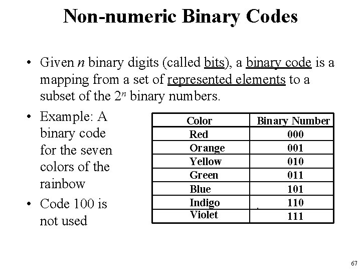
Non-numeric Binary Codes • Given n binary digits (called bits), a binary code is a mapping from a set of represented elements to a subset of the 2 n binary numbers. • Example: A Binary Number Color binary code Red 000 Orange 001 for the seven Yellow 010 colors of the Green 011 rainbow Blue 101 Indigo 110 • Code 100 is Violet 111 not used 67

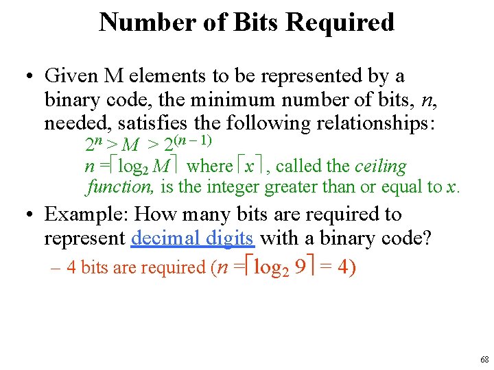
Number of Bits Required • Given M elements to be represented by a binary code, the minimum number of bits, n, needed, satisfies the following relationships: 2 n > M > 2(n – 1) n = log 2 M where x , called the ceiling function, is the integer greater than or equal to x. • Example: How many bits are required to represent decimal digits with a binary code? – 4 bits are required (n = log 2 9 = 4) 68

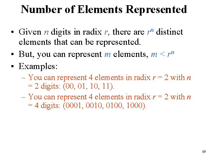
Number of Elements Represented • Given n digits in radix r, there are rn distinct elements that can be represented. • But, you can represent m elements, m < rn • Examples: – You can represent 4 elements in radix r = 2 with n = 2 digits: (00, 01, 10, 11). – You can represent 4 elements in radix r = 2 with n = 4 digits: (0001, 0010, 0100, 1000). 69

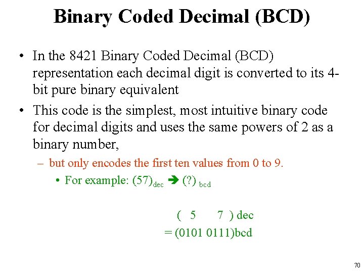
Binary Coded Decimal (BCD) • In the 8421 Binary Coded Decimal (BCD) representation each decimal digit is converted to its 4 bit pure binary equivalent • This code is the simplest, most intuitive binary code for decimal digits and uses the same powers of 2 as a binary number, – but only encodes the first ten values from 0 to 9. • For example: (57)dec (? ) bcd ( 5 7 ) dec = (0101 0111)bcd 70

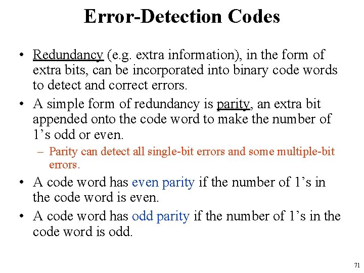
Error-Detection Codes • Redundancy (e. g. extra information), in the form of extra bits, can be incorporated into binary code words to detect and correct errors. • A simple form of redundancy is parity, an extra bit appended onto the code word to make the number of 1’s odd or even. – Parity can detect all single-bit errors and some multiple-bit errors. • A code word has even parity if the number of 1’s in the code word is even. • A code word has odd parity if the number of 1’s in the code word is odd. 71

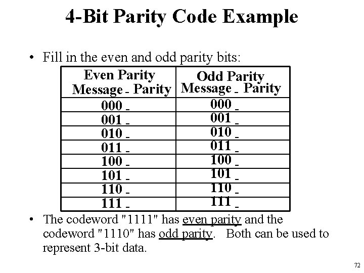
4 -Bit Parity Code Example • Fill in the even and odd parity bits: Even Parity Odd Parity Message - Parity 000 001 010 011 100 101 110 111 - • The codeword "1111" has even parity and the codeword "1110" has odd parity. Both can be used to represent 3 -bit data. 72

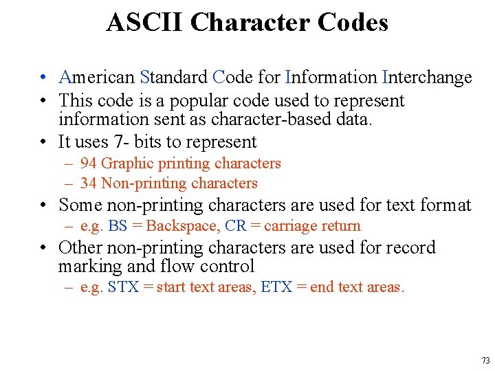
ASCII Character Codes • American Standard Code for Information Interchange • This code is a popular code used to represent information sent as character-based data. • It uses 7 - bits to represent – 94 Graphic printing characters – 34 Non-printing characters • Some non-printing characters are used for text format – e. g. BS = Backspace, CR = carriage return • Other non-printing characters are used for record marking and flow control – e. g. STX = start text areas, ETX = end text areas. 73

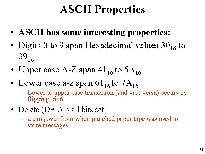
ASCII Properties • ASCII has some interesting properties: • Digits 0 to 9 span Hexadecimal values 3016 to 3916 • Upper case A-Z span 4116 to 5 A 16 • Lower case a-z span 6116 to 7 A 16 – Lower to upper case translation (and vice versa) occurs by flipping bit 6 • Delete (DEL) is all bits set, – a carryover from when punched paper tape was used to store messages 74

UNICODE • UNICODE extends ASCII to 65, 536 universal characters codes – For encoding characters in world languages – Available in many modern applications – 2 byte (16 -bit) code words 75

Warning: Conversion or Coding? • Do NOT mix up "conversion of a decimal number to a binary number" with "coding a decimal number with a binary code". • 1310 = 11012 – This is conversion • 13 0001 0011 BCD – This is coding 76

Another use for bits: Logic • Beyond numbers – logical variables can be true or false, on or off, etc. , and so are readily represented by the binary system. – A logical variable A can take the values false = 0 or true = 1 only. – The manipulation of logical variables is known as Boolean Algebra, and has its own set of operations • which are not to be confused with the arithmetical operations. – Some basic operations: NOT, AND, OR, XOR 77

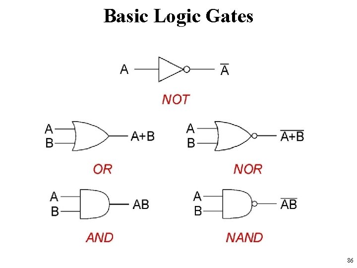
Binary Logic and Gates • Binary variables take on one of two values. • Logical operators operate on binary values and binary variables. • Basic logical operators are the logic functions AND, OR and NOT. • Logic gates implement logic functions. • Boolean Algebra: a useful mathematical system for specifying and transforming logic functions. • We study Boolean algebra as foundation for designing and analyzing digital systems! 78

Binary Variables • Recall that the two binary values have different names: – True/False – On/Off – Yes/No – 1/0 • We use 1 and 0 to denote the two values. • Variable identifier examples: – A, B, y, z, or X 1 for now – RESET, START_IT, or ADD 1 later 79

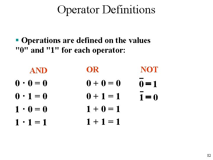
Logical Operations • The three basic logical operations are: – AND – OR – NOT • AND is denoted by a dot (·) • OR is denoted by a plus (+) • NOT is denoted by an overbar ( ¯ ), a single quote mark (') after, or (~) before the variable 80

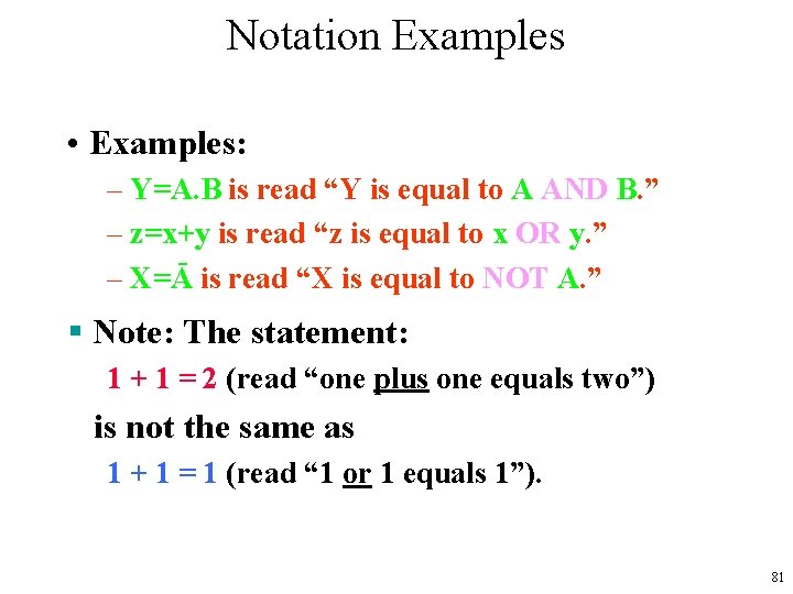
Notation Examples • Examples: – Y=A. B is read “Y is equal to A AND B. ” – z=x+y is read “z is equal to x OR y. ” – X=Ā is read “X is equal to NOT A. ” § Note: The statement: 1 + 1 = 2 (read “one plus one equals two”) is not the same as 1 + 1 = 1 (read “ 1 or 1 equals 1”). 81

Operator Definitions § Operations are defined on the values "0" and "1" for each operator: AND 0· 0=0 0· 1=0 1· 0=0 1· 1=1 OR NOT 0+0=0 0+1=1 1+0=1 1+1=1 0=1 1=0 82

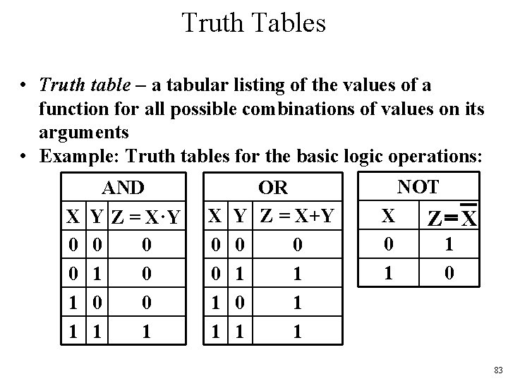
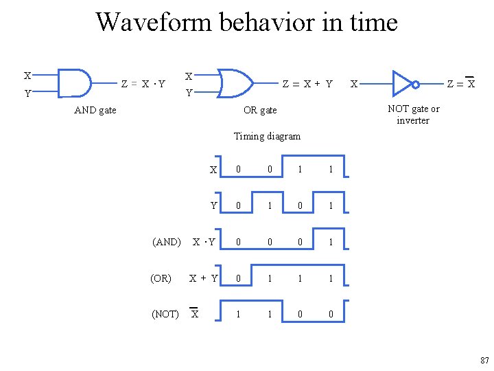
Truth Tables • Truth table - a tabular listing of the values of a function for all possible combinations of values on its arguments • Example: Truth tables for the basic logic operations: X 0 0 1 1 AND Y Z = X·Y 0 0 1 0 0 0 1 1 X 0 0 1 1 Y 0 1 OR Z = X+Y 0 1 1 1 NOT X 0 1 Z=X 1 0 83

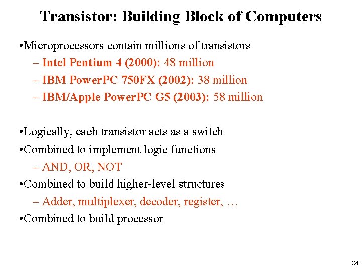
Transistor: Building Block of Computers • Microprocessors contain millions of transistors – Intel Pentium 4 (2000): 48 million – IBM Power. PC 750 FX (2002): 38 million – IBM/Apple Power. PC G 5 (2003): 58 million • Logically, each transistor acts as a switch • Combined to implement logic functions – AND, OR, NOT • Combined to build higher-level structures – Adder, multiplexer, decoder, register, … • Combined to build processor 84

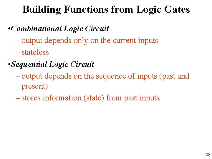
Building Functions from Logic Gates • Combinational Logic Circuit – output depends only on the current inputs – stateless • Sequential Logic Circuit – output depends on the sequence of inputs (past and present) – stores information (state) from past inputs 85

Basic Logic Gates 86

Waveform behavior in time X Z = X ·Y Y X Z= X+ Y Y Z= X NOT gate or inverter OR gate AND gate X Timing diagram X 0 0 1 1 Y 0 1 X ·Y 0 0 0 1 (OR) X+ Y 0 1 1 1 (NOT) X 1 1 0 0 (AND) 87

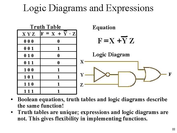
Logic Diagrams and Expressions Truth Table XYZ 000 001 010 011 100 101 110 111 F = X + Y ×Z 0 1 0 X 0 1 Y 1 1 Z 1 Equation F = X +Y Z Logic Diagram F • Boolean equations, truth tables and logic diagrams describe the same function! • Truth tables are unique; expressions and logic diagrams are not. This gives flexibility in implementing functions. 88

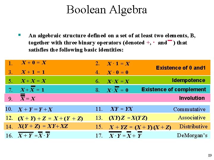
Boolean Algebra § 1. 3. 5. 7. 9. An algebraic structure defined on a set of at least two elements, B, together with three binary operators (denoted +, · and ) that satisfies the following basic identities: X+0= X X+1 =1 X+X =X X+X =1 X=X 10. X + Y = Y + X 12. (X + Y) + Z = X + (Y + Z) 14. X(Y + Z) = XY + XZ 16. X + Y = X. Y 2. 4. 6. 8. X. 1 =X X 0 =0. Existence of 0 and 1 X. X = X Idempotence X. X = 0 Existence of complement Involution 11. XY = YX Commutative Associative 13. (XY) Z = X(YZ) 15. X + YZ = (X + Y) (X + Z) Distributive De. Morgan’s 17. X. Y = X + Y 89

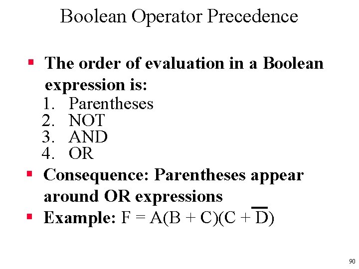
Boolean Operator Precedence § The order of evaluation in a Boolean expression is: 1. Parentheses 2. NOT 3. AND 4. OR § Consequence: Parentheses appear around OR expressions § Example: F = A(B + C)(C + D) 90

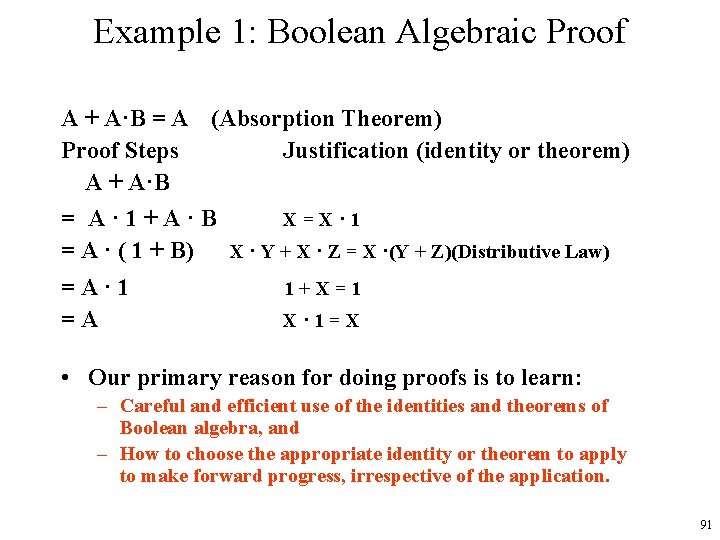
Example 1: Boolean Algebraic Proof A + A·B = A (Absorption Theorem) Proof Steps Justification (identity or theorem) A + A·B = A· 1+A·B X=X· 1 = A · ( 1 + B) X · Y + X · Z = X ·(Y + Z)(Distributive Law) =A· 1 =A 1+X=1 X· 1=X • Our primary reason for doing proofs is to learn: – Careful and efficient use of the identities and theorems of Boolean algebra, and – How to choose the appropriate identity or theorem to apply to make forward progress, irrespective of the application. 91

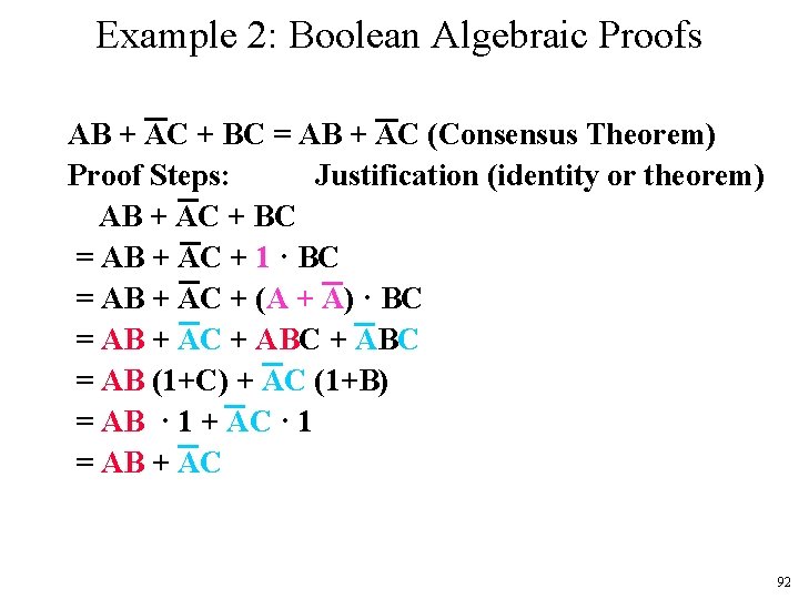
Example 2: Boolean Algebraic Proofs AB + AC + BC = AB + AC (Consensus Theorem) Proof Steps: Justification (identity or theorem) AB + AC + BC = AB + AC + 1 · BC = AB + AC + (A + A) · BC = AB + AC + ABC = AB (1+C) + AC (1+B) = AB · 1 + AC · 1 = AB + AC 92

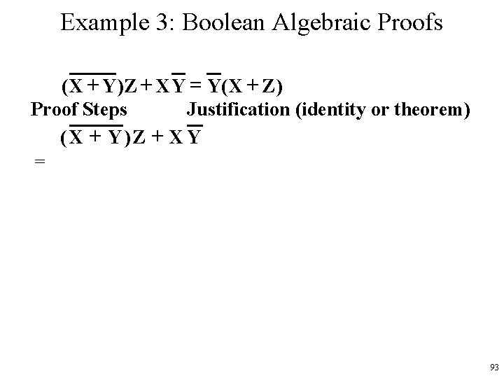
Example 3: Boolean Algebraic Proofs ( X + Y ) Z + X Y = Y( X + Z ) Proof Steps Justification (identity or theorem) ( X + Y )Z + X Y = 93

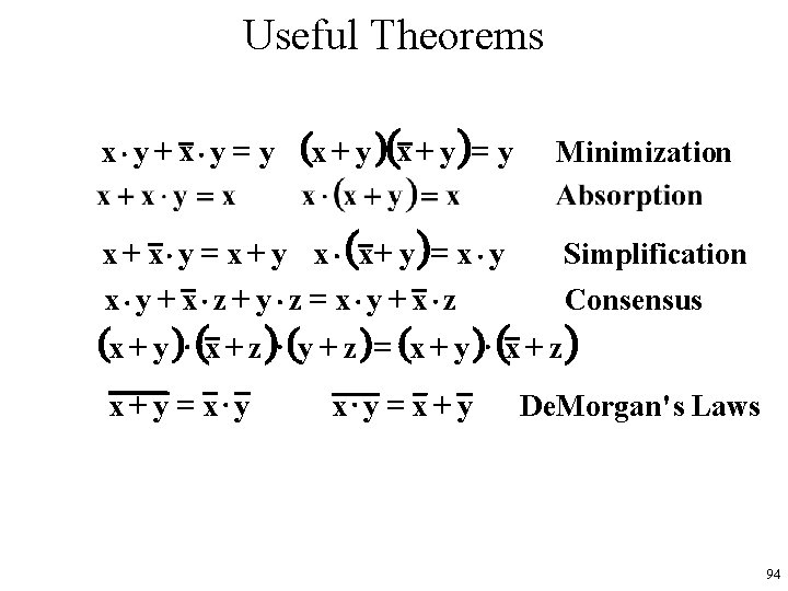
Useful Theorems x×y + x×y = y (x + y )= y Minimization x + x × y = x + y x × (x + y )= x × y Simplification x×y + x×z + y×z = x×y + x×z Consensus (x + y )× (x + z )× (y + z ) = (x + y )× (x + z ) x + y = x×y = x + y De. Morgan' s Laws 94

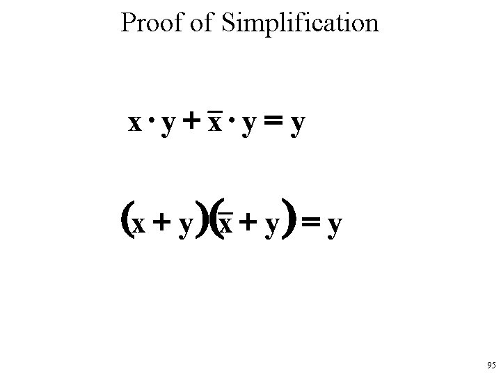
Proof of Simplification x×y + x×y = y (x + y ) = y 95

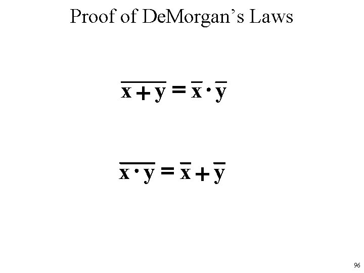
Proof of De. Morgan’s Laws x + y = x×y = x + y 96

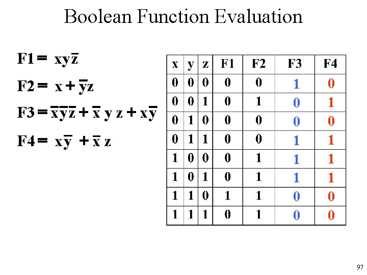
Boolean Function Evaluation F 1 = xy z F 2 = x + yz F 3 = x y z + x y F 4 = x y + x z 1 0 0 1 1 1 0 0 97

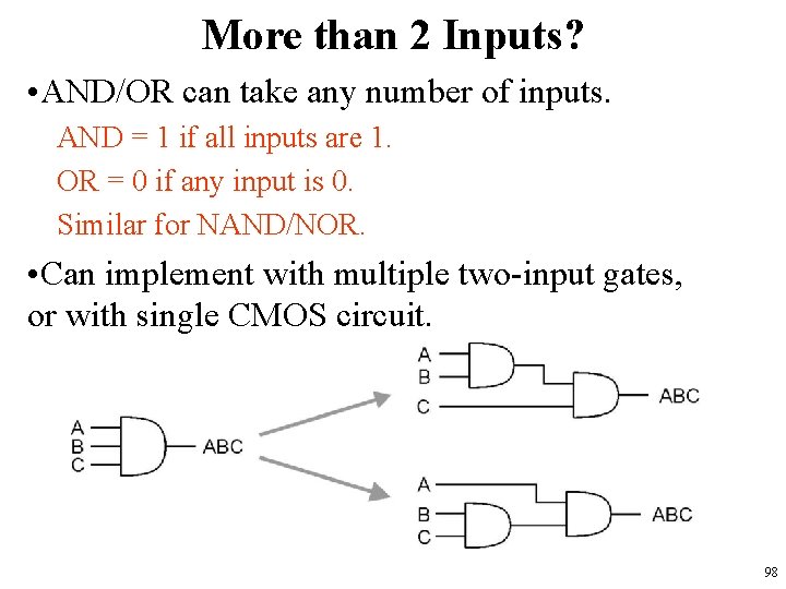
More than 2 Inputs? • AND/OR can take any number of inputs. AND = 1 if all inputs are 1. OR = 0 if any input is 0. Similar for NAND/NOR. • Can implement with multiple two-input gates, or with single CMOS circuit. 98

Functions and Functional Blocks • The functions considered are those found to be very useful in design • Corresponding to each of the functions is a combinational circuit implementation called a functional block. • In the past, many functional blocks were implemented as SSI, MSI, and LSI circuits. • Today, they are often simply parts within a VLSI circuit. 99

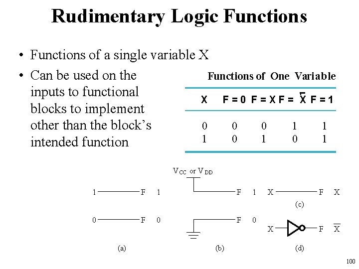
Rudimentary Logic Functions • Functions of a single variable X • Can be used on the Functions of One Variab le inputs to functional X F=0 F=XF= X F=1 blocks to implement 0 0 0 1 1 other than the block’s 1 0 1 intended function V CC or V DD 1 F 1 X F X (c) 0 F 0 X (a) (b) (d) 100

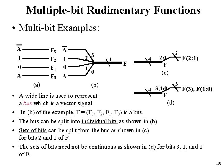
Multiple-bit Rudimentary Functions • Multi-bit Examples: A 1 0 A F 3 A F 2 1 F 1 0 F 0 A (a) 2 1 3 0 (b) 4 F 4 2: 1 2 F (c) 4 3, 1: 0 3 F(2: 1) F(3), F(1: 0) F • A wide line is used to represent (d) a bus which is a vector signal • In (b) of the example, F = (F 3, F 2, F 1, F 0) is a bus. • The bus can be split into individual bits as shown in (b) • Sets of bits can be split from the bus as shown in (c) for bits 2 and 1 of F. • The sets of bits need not be continuous as shown in (d) for bits 3, 1, and 0 of F. 101

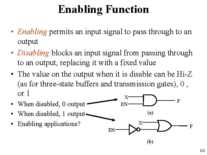
Enabling Function • Enabling permits an input signal to pass through to an output • Disabling blocks an input signal from passing through to an output, replacing it with a fixed value • The value on the output when it is disable can be Hi-Z (as for three-state buffers and transmission gates), 0 , or 1 X • When disabled, 0 output • When disabled, 1 output • Enabling applications? F EN (a) X F EN (b) 102

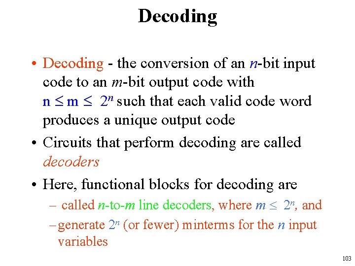
Decoding • Decoding - the conversion of an n-bit input code to an m-bit output code with n m 2 n such that each valid code word produces a unique output code • Circuits that perform decoding are called decoders • Here, functional blocks for decoding are – called n-to-m line decoders, where m 2 n, and – generate 2 n (or fewer) minterms for the n input variables 103

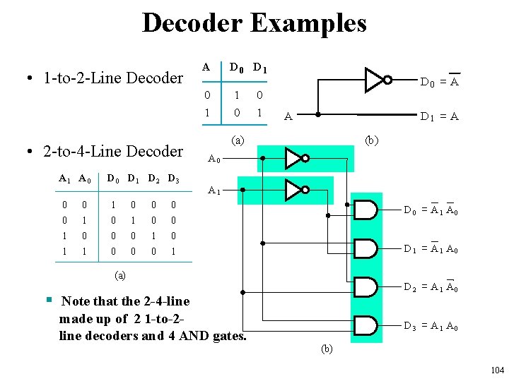
Decoder Examples • 1 -to-2 -Line Decoder A 0 1 • 2 -to-4 -Line Decoder A 1 A 0 0 0 1 1 0 1 D 0 D 1 D 2 D 3 1 0 0 0 0 1 0 D 1 1 0 0 1 D 0 = A D 1 = A A (a) (b) A 0 A 1 0 0 0 1 D 0 = A 1 A 0 D 1 = A 1 A 0 (a) D 2 = A 1 A 0 § Note that the 2 -4 -line made up of 2 1 -to-2 line decoders and 4 AND gates. D 3 = A 1 A 0 (b) 104

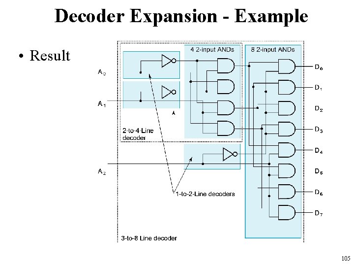
Decoder Expansion - Example • Result 105

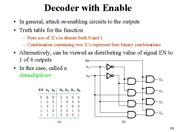
Decoder with Enable • In general, attach m-enabling circuits to the outputs • Truth table for the function – Note use of X’s to denote both 0 and 1 – Combination containing two X’s represent four binary combinations • Alternatively, can be viewed as distributing value of signal EN to 1 of 4 outputs EN A • In this case, called a A demultiplexer 1 0 EN A 1 A 0 0 1 1 X 0 1 D 0 D 1 D 2 D 3 0 1 0 0 0 (a) 0 0 1 0 D 1 0 0 1 D 2 D 3 (b) 106

Encoding • Encoding - the opposite of decoding - the conversion of an m-bit input code to a n-bit output code with n m 2 n such that each valid code word produces a unique output code • Circuits that perform encoding are called encoders • An encoder has 2 n (or fewer) input lines and n output lines which generate the binary code corresponding to the input values • Typically, an encoder converts a code containing exactly one bit that is 1 to a binary code corresponding to the position in which the 1 appears. 107

Selecting • Selecting of data or information is a critical function in digital systems and computers • Circuits that perform selecting have: – A set of information inputs from which the selection is made – A single output – A set of control lines for making the selection • Logic circuits that perform selecting are called multiplexers • Selecting can also be done by three-state logic or transmission gates 108

Multiplexers • A multiplexer selects information from an input line and directs the information to an output line • A typical multiplexer has n control inputs (Sn - 1, … S 0) called selection inputs, 2 n information inputs (I 2 n - 1, … I 0), and one output Y • A multiplexer can be designed to have m information inputs with m < 2 n as well as n selection inputs 109

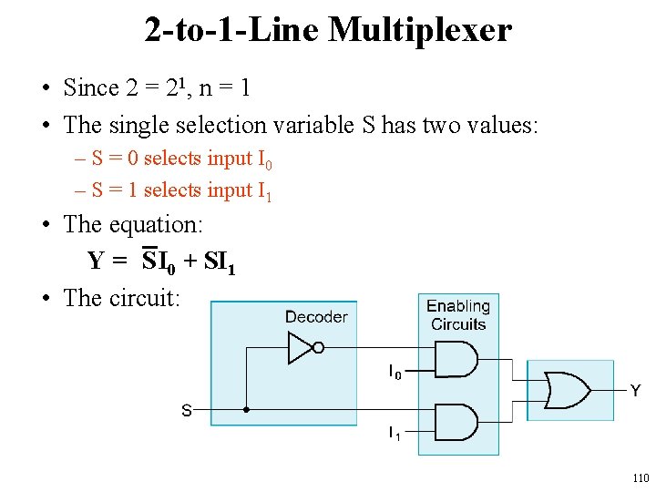
2 -to-1 -Line Multiplexer • Since 2 = 21, n = 1 • The single selection variable S has two values: – S = 0 selects input I 0 – S = 1 selects input I 1 • The equation: Y = S I 0 + SI 1 • The circuit: 110

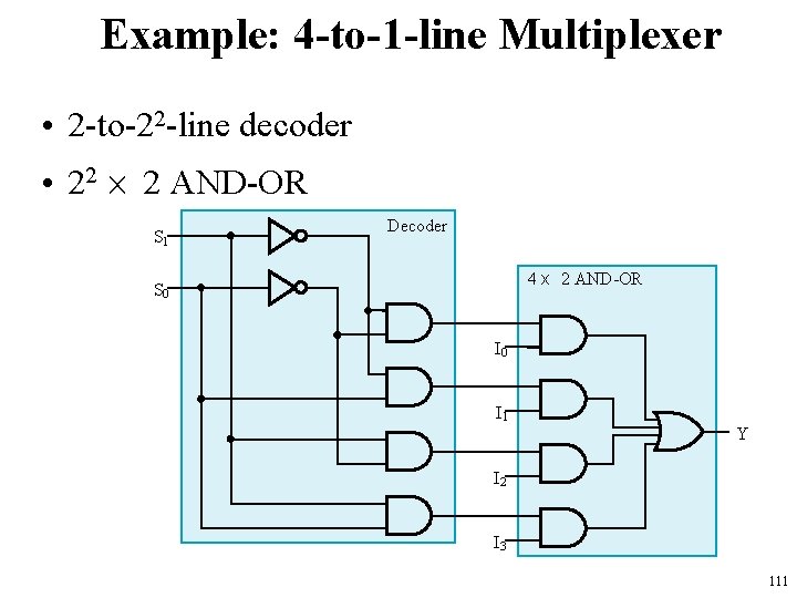
Example: 4 -to-1 -line Multiplexer • 2 -to-22 -line decoder • 22 2 AND-OR Decoder S 1 4 x 2 AND-OR S 0 S 1 S 0 Decoder I 0 I 1 Y Y I 2 I 3 111

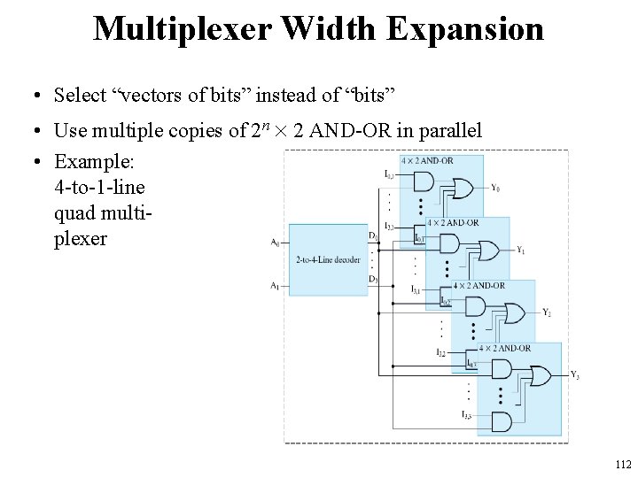
Multiplexer Width Expansion • Select “vectors of bits” instead of “bits” • Use multiple copies of 2 n 2 AND-OR in parallel • Example: 4 -to-1 -line quad multiplexer 112

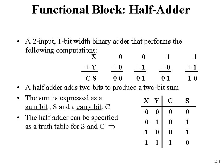
Functional Blocks: Addition • Binary addition used frequently • Addition Development: – Half-Adder (HA), a 2 -input bit-wise addition functional block, – Full-Adder (FA), a 3 -input bit-wise addition functional block, – Ripple Carry Adder, an iterative array to perform binary addition, and – Carry-Look-Ahead Adder (CLA), a hierarchical structure to improve performance. 113

Functional Block: Half-Adder • A 2 -input, 1 -bit width binary adder that performs the following computations: X +Y 0 +0 0 +1 1 +0 CS 00 01 01 • A half adder adds two bits to produce a two-bit sum • The sum is expressed as a sum bit , S and a carry bit, C • The half adder can be specified as a truth table for S and C 1 +1 10 X Y C S 0 0 1 1 0 0 0 1 0 1 114

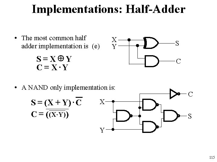
Implementations: Half-Adder • The most common half adder implementation is (e) X Y S = XÅY C = X×Y C • A NAND only implementation is: S = ( X + Y) × C C = ( ( X ×Y ) ) S X C S Y 115

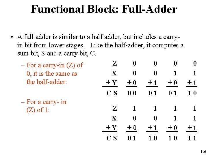
Functional Block: Full-Adder • A full adder is similar to a half adder, but includes a carryin bit from lower stages. Like the half-adder, it computes a sum bit, S and a carry bit, C. Z 0 0 0 – For a carry-in (Z) of X 0 0 1 0, it is the same as the half-adder: +Y +0 +1 +0 CS 00 01 01 – For a carry- in Z 1 1 1 (Z) of 1: X 0 0 1 +Y +0 +1 +0 CS 01 10 10 0 1 +1 10 1 1 +1 11 116

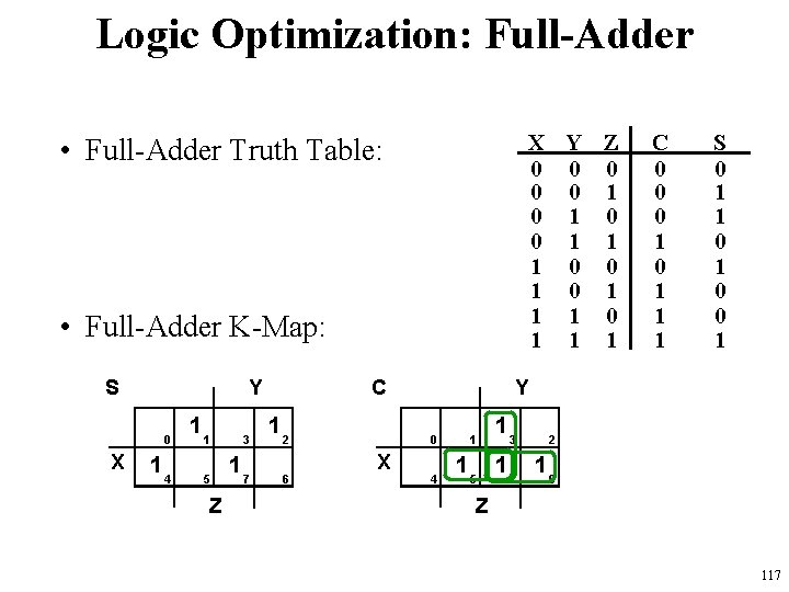
Logic Optimization: Full-Adder X Y Z 0 0 0 1 1 1 0 0 1 1 1 • Full-Adder Truth Table: • Full-Adder K-Map: S Y 0 X 14 11 3 5 17 Z C 12 6 S 0 1 1 0 0 1 Y 0 X C 0 0 0 1 1 1 4 1 13 2 15 17 16 Z 117

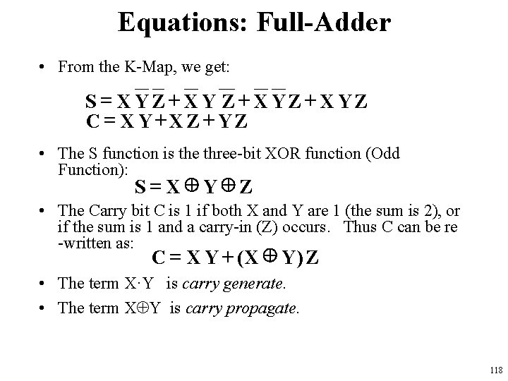
Equations: Full-Adder • From the K-Map, we get: S = XYZ+ XYZ C = XY+XZ+YZ • The S function is the three-bit XOR function (Odd Function): S = XÅYÅZ • The Carry bit C is 1 if both X and Y are 1 (the sum is 2), or if the sum is 1 and a carry-in (Z) occurs. Thus C can be re -written as: C = X Y + ( X Å Y) Z • The term X·Y is carry generate. • The term X Y is carry propagate. 118

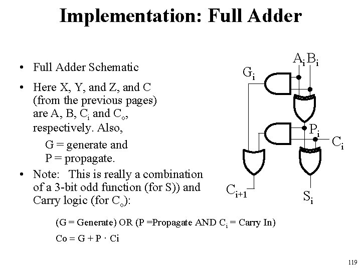
Implementation: Full Adder • Full Adder Schematic • Here X, Y, and Z, and C (from the previous pages) are A, B, Ci and Co, respectively. Also, G = generate and P = propagate. • Note: This is really a combination of a 3 -bit odd function (for S)) and Carry logic (for Co): Gi Ai B i Pi Ci+1 Ci Si (G = Generate) OR (P =Propagate AND Ci = Carry In) Co = G + P · Ci 119

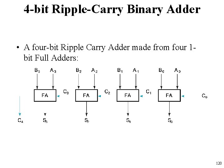
4 -bit Ripple-Carry Binary Adder • A four-bit Ripple Carry Adder made from four 1 bit Full Adders: 120

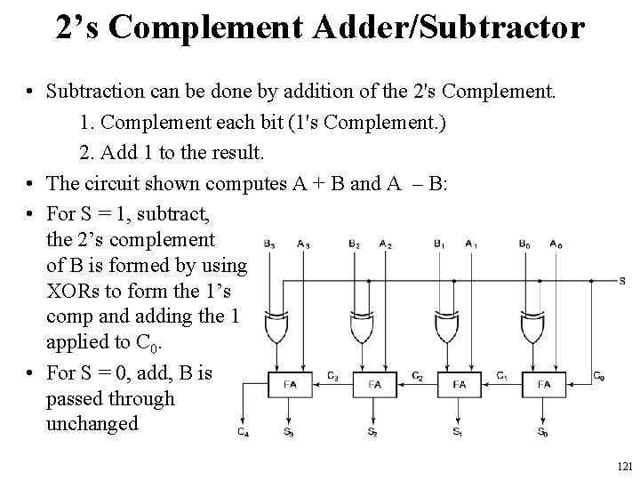
2’s Complement Adder/Subtractor • Subtraction can be done by addition of the 2's Complement. 1. Complement each bit (1's Complement. ) 2. Add 1 to the result. • The circuit shown computes A + B and A – B: • For S = 1, subtract, the 2’s complement of B is formed by using XORs to form the 1’s comp and adding the 1 applied to C 0. • For S = 0, add, B is passed through unchanged 121

Combinational vs. Sequential • Combinational Circuit – always gives the same output for a given set of inputs • ex: adder always generates sum and carry, regardless of previous inputs • Sequential Circuit – stores information – output depends on stored information (state) plus input • so a given input might produce different outputs, depending on the stored information 122

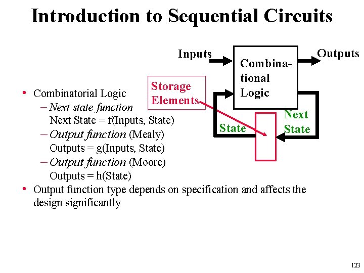
Introduction to Sequential Circuits Inputs • Combinatorial Logic – Next state function Storage Elements Combinational Logic Outputs Next State = f(Inputs, State) State – Output function (Mealy) Outputs = g(Inputs, State) – Output function (Moore) Outputs = h(State) • Output function type depends on specification and affects the designificantly 123

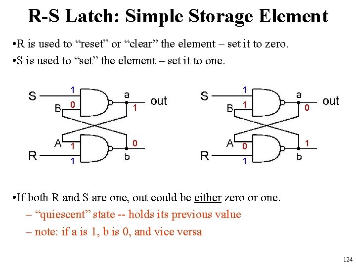
R-S Latch: Simple Storage Element • R is used to “reset” or “clear” the element – set it to zero. • S is used to “set” the element – set it to one. 1 1 0 0 1 1 • If both R and S are one, out could be either zero or one. – “quiescent” state -- holds its previous value – note: if a is 1, b is 0, and vice versa 124

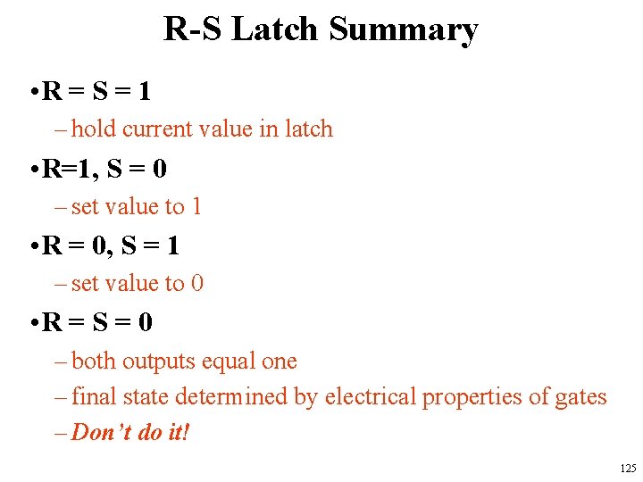
R-S Latch Summary • R = S = 1 – hold current value in latch • R=1, S = 0 – set value to 1 • R = 0, S = 1 – set value to 0 • R = S = 0 – both outputs equal one – final state determined by electrical properties of gates – Don’t do it! 125

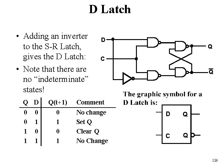
D Latch • Adding an inverter to the S-R Latch, gives the D Latch: • Note that there are no “indeterminate” states! Q 0 0 1 1 D 0 1 Q(t+1) 0 1 D Q C Comment No change Set Q Clear Q No Change Q D Q C Q 126

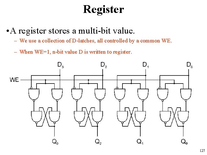
Register • A register stores a multi-bit value. – We use a collection of D-latches, all controlled by a common WE. – When WE=1, n-bit value D is written to register. 127

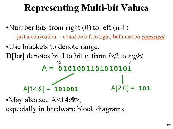
Representing Multi-bit Values • Number bits from right (0) to left (n-1) – just a convention -- could be left to right, but must be consistent • Use brackets to denote range: D[l: r] denotes bit l to bit r, from left to right 0 15 A = 010100110101 A[14: 9] = 101001 A[2: 0] = 101 • May also see A<14: 9>, especially in hardware block diagrams. 128

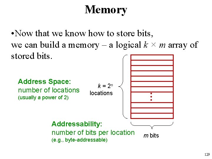
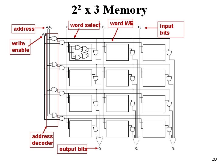
Memory • Now that we know how to store bits, we can build a memory – a logical k × m array of stored bits. Address Space: number of locations (usually a power of 2) k = 2 n locations Addressability: number of bits per location (e. g. , byte-addressable) • • • m bits 129

22 x 3 Memory address word select word WE input bits write enable address decoder output bits 130

More Memory Details • This is a not the way actual memory is implemented. – fewer transistors, much more dense, relies on electrical properties • But the logical structure is very similar. – address decoder – word select line – word write enable • Two basic kinds of RAM (Random Access Memory) • Static RAM (SRAM) – fast, maintains data as long as power applied • Dynamic RAM (DRAM) – slower but denser, bit storage decays – must be periodically refreshed Also, non-volatile memories: ROM, PROM, flash, … 131

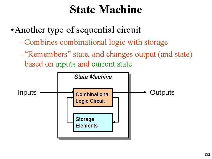
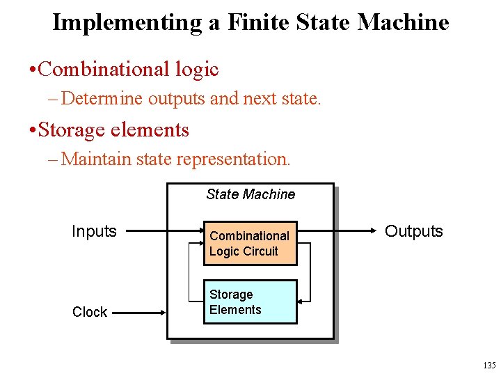
State Machine • Another type of sequential circuit – Combines combinational logic with storage – “Remembers” state, and changes output (and state) based on inputs and current state State Machine Inputs Combinational Logic Circuit Outputs Storage Elements 132

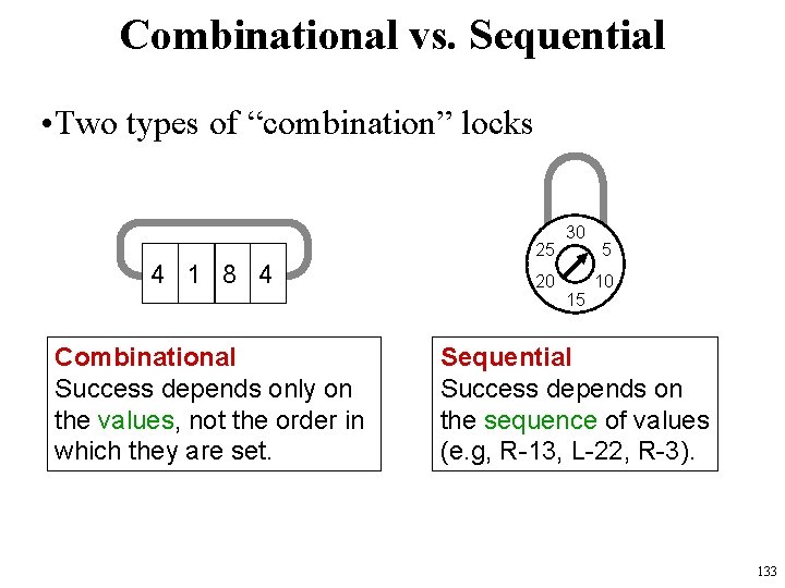
Combinational vs. Sequential • Two types of “combination” locks 25 4 1 8 4 Combinational Success depends only on the values, not the order in which they are set. 20 30 15 5 10 Sequential Success depends on the sequence of values (e. g, R-13, L-22, R-3). 133

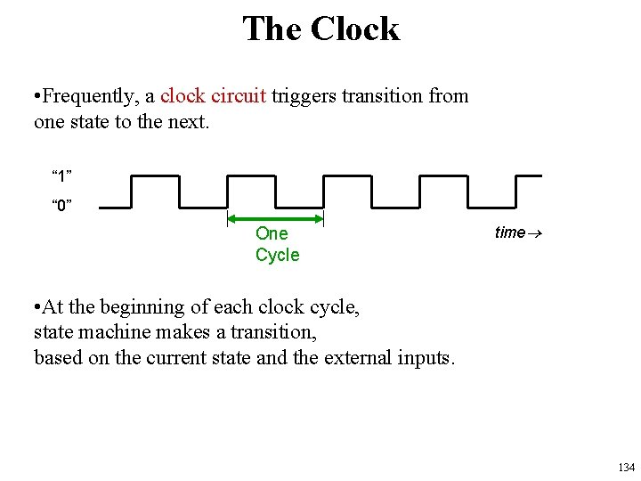
The Clock • Frequently, a clock circuit triggers transition from one state to the next. “ 1” “ 0” One Cycle time • At the beginning of each clock cycle, state machine makes a transition, based on the current state and the external inputs. 134

Implementing a Finite State Machine • Combinational logic – Determine outputs and next state. • Storage elements – Maintain state representation. State Machine Inputs Clock Combinational Logic Circuit Outputs Storage Elements 135

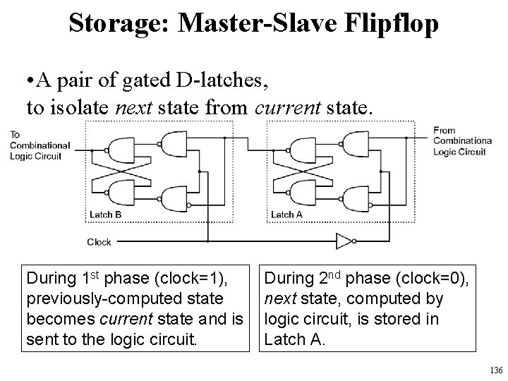
Storage: Master-Slave Flipflop • A pair of gated D-latches, to isolate next state from current state. During 1 st phase (clock=1), previously-computed state becomes current state and is sent to the logic circuit. During 2 nd phase (clock=0), next state, computed by logic circuit, is stored in Latch A. 136

Storage • Each master-slave flipflop stores one state bit. • The number of storage elements (flipflops) needed is determined by the number of states (and the representation of each state). • Examples: – Sequential lock • Four states – two bits 137

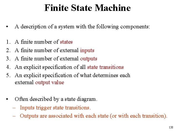
Finite State Machine • A description of a system with the following components: 1. 2. 3. 4. 5. A finite number of states A finite number of external inputs A finite number of external outputs An explicit specification of all state transitions An explicit specification of what determines each external output value • Often described by a state diagram. – Inputs trigger state transitions. – Outputs are associated with each state (or with each transition). 138

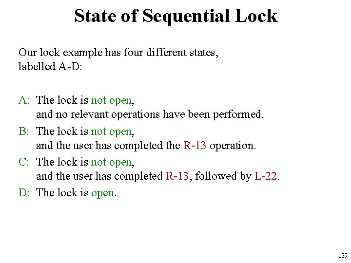
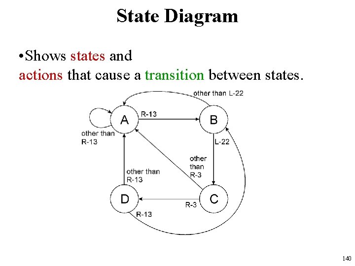
State of Sequential Lock Our lock example has four different states, labelled A-D: A: The lock is not open, and no relevant operations have been performed. B: The lock is not open, and the user has completed the R-13 operation. C: The lock is not open, and the user has completed R-13, followed by L-22. D: The lock is open. 139

State Diagram • Shows states and actions that cause a transition between states. 140

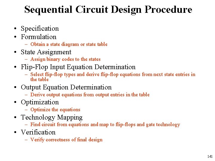
Sequential Circuit Design Procedure • Specification • Formulation – Obtain a state diagram or state table • State Assignment – Assign binary codes to the states • Flip-Flop Input Equation Determination – Select flip-flop types and derive flip-flop equations from next state entries in the table • Output Equation Determination – Derive output equations from output entries in the table • Optimization – Optimize the equations • Technology Mapping – Find circuit from equations and map to flip-flops and gate technology • Verification – Verify correctness of final design 141

Example: Sequence Recognizer Procedure • To develop a sequence recognizer state diagram: – Begin in an initial state in which NONE of the initial portion of the sequence has occurred (typically “reset” state). – Add a state that recognizes that the first symbol has occurred. – Add states that recognize each successive symbol occurring. – The final state represents the input sequence (possibly less the final input value) occurence. – Add state transition arcs which specify what happens when a symbol not in the proper sequence has occurred. – Add other arcs on non-sequence inputs which transition to states that represent the input subsequence that has occurred. • The last step is required because the circuit must recognize the input sequence regardless of where it occurs within the overall sequence applied since “reset. ”. 142

State Assignment • Each of the m states must be assigned a unique code • Minimum number of bits required is n such that n ≥ log 2 m where x is the smallest integer ≥ x • There are useful state assignments that use more than the minimum number of bits • There are 2 n - m unused states 143

Sequence Recognizer Example • Example: Recognize the sequence 1101 – Note that the sequence 1111101 contains 1101 and "11" is a proper sub-sequence of the sequence. • Thus, the sequential machine must remember that the first two one's have occurred as it receives another symbol. • Also, the sequence 1101101 contains 1101 as both an initial subsequence and a final subsequence with some overlap, i. e. , 1101101 or 1101101. • And, the 1 in the middle, 1101101, is in both subsequences. • The sequence 1101 must be recognized each time it occurs in the input sequence. 144

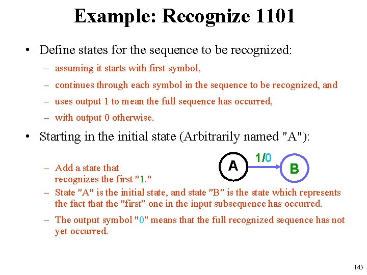
Example: Recognize 1101 • Define states for the sequence to be recognized: – assuming it starts with first symbol, – continues through each symbol in the sequence to be recognized, and – uses output 1 to mean the full sequence has occurred, – with output 0 otherwise. • Starting in the initial state (Arbitrarily named "A"): 1/0 A – Add a state that B recognizes the first "1. " – State "A" is the initial state, and state "B" is the state which represents the fact that the "first" one in the input subsequence has occurred. – The output symbol "0" means that the full recognized sequence has not yet occurred. 145

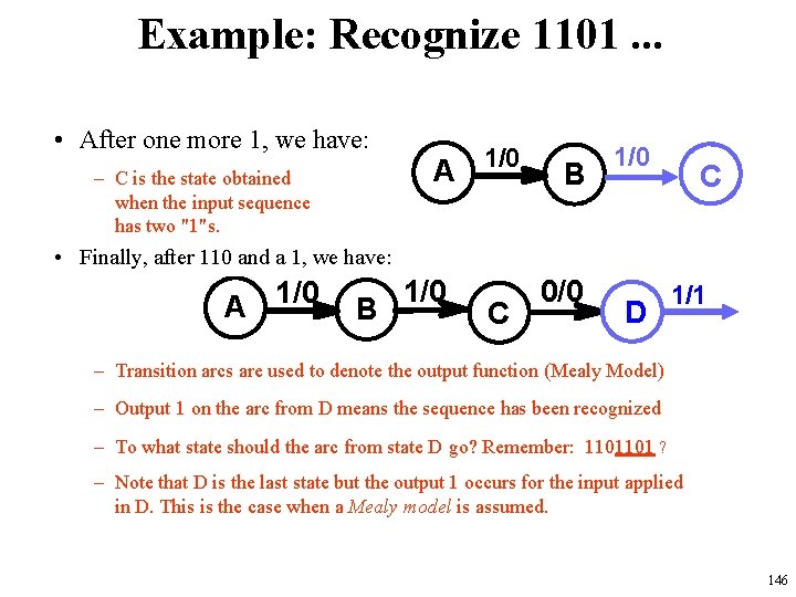
Example: Recognize 1101. . . • After one more 1, we have: – C is the state obtained when the input sequence has two "1"s. A 1/0 B 1/0 C • Finally, after 110 and a 1, we have: A 1/0 B 1/0 C 0/0 D 1/1 – Transition arcs are used to denote the output function (Mealy Model) – Output 1 on the arc from D means the sequence has been recognized – To what state should the arc from state D go? Remember: 1101101 ? – Note that D is the last state but the output 1 occurs for the input applied in D. This is the case when a Mealy model is assumed. 146

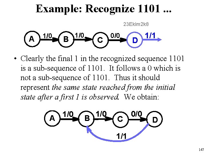
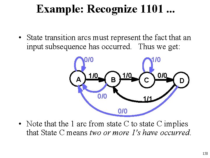
Example: Recognize 1101. . . 23 Ekim 2 k 8 A 1/0 B 1/0 C 0/0 D 1/1 • Clearly the final 1 in the recognized sequence 1101 is a sub-sequence of 1101. It follows a 0 which is not a sub-sequence of 1101. Thus it should represent the same state reached from the initial state after a first 1 is observed. We obtain: A 1/0 B 1/0 C 0/0 D 1/1 147

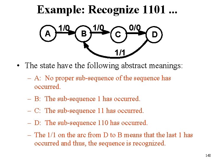
Example: Recognize 1101. . . A 1/0 B 1/0 C 0/0 D 1/1 • The state have the following abstract meanings: – A: No proper sub-sequence of the sequence has occurred. – B: The sub-sequence 1 has occurred. – C: The sub-sequence 11 has occurred. – D: The sub-sequence 110 has occurred. – The 1/1 on the arc from D to B means that the last 1 has occurred and thus, the sequence is recognized. 148

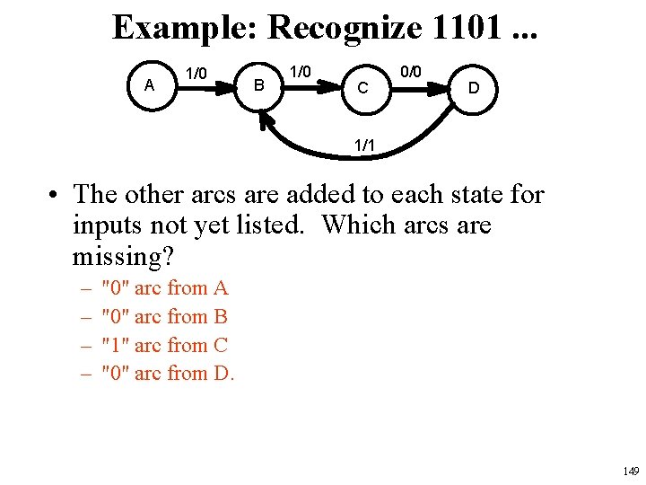
Example: Recognize 1101. . . A 1/0 B 1/0 C 0/0 D 1/1 • The other arcs are added to each state for inputs not yet listed. Which arcs are missing? – – "0" arc from A "0" arc from B "1" arc from C "0" arc from D. 149

Example: Recognize 1101. . . • State transition arcs must represent the fact that an input subsequence has occurred. Thus we get: 0/0 A 1/0 B 1/0 0/0 C 0/0 D 1/1 0/0 • Note that the 1 arc from state C to state C implies that State C means two or more 1's have occurred. 150

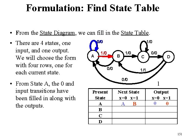
Formulation: Find State Table • From the State Diagram, we can fill in the State Table. • There are 4 states, one input, and one output. We will choose the form with four rows, one for each current state. • From State A, the 0 and input transitions have been filled in along with the outputs. 0/0 A 1/0 1/0 B C 0/0 1/1 0/0 Present State A B C D D 1 Next State x=0 x=1 A B Output x=0 x=1 0 0 151

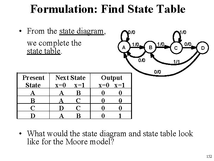
Formulation: Find State Table • From the state diagram, we complete the state table. 0/0 A 1/0 B 1/0 0/0 Present State A B C D Next State x=0 x=1 A B A C D C A B Output x=0 x=1 0 0 0 0 1 C 0/0 D 1/1 0/0 • What would the state diagram and state table look like for the Moore model? 152

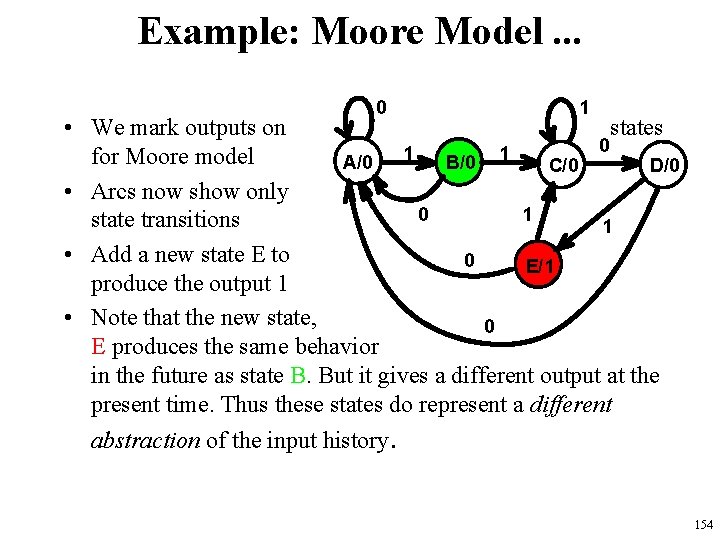
Example: Moore Model for Sequence 1101 • For the Moore Model, outputs are associated with states. • We need to add a state "E" with output value 1 for the final 1 in the recognized input sequence. – This new state E, though similar to B, would generate an output of 1 and thus be different from B. • The Moore model for a sequence recognizer usually has more states than the Mealy model. 153

Example: Moore Model. . . 0 1 • We mark outputs on states 0 1 1 for Moore model A/0 B/0 C/0 D/0 • Arcs now show only 0 1 state transitions 1 • Add a new state E to 0 E/1 produce the output 1 • Note that the new state, 0 E produces the same behavior in the future as state B. But it gives a different output at the present time. Thus these states do represent a different abstraction of the input history. 154

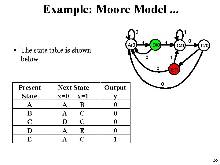
Example: Moore Model. . . 0 A/0 • The state table is shown below 1 1 B/0 1 0 Present State A B C D E Next State x=0 x=1 A B A C D C A E A C Output y 0 0 1 C/0 0 D/0 1 E/1 0 155

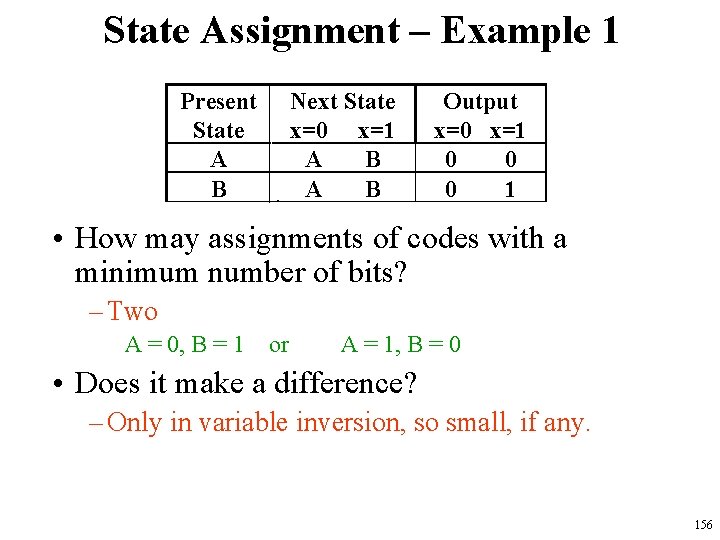
State Assignment – Example 1 Present State A B Next State x=0 x=1 A B Output x=0 x=1 0 0 0 1 • How may assignments of codes with a minimum number of bits? – Two A = 0, B = 1 or A = 1, B = 0 • Does it make a difference? – Only in variable inversion, so small, if any. 156

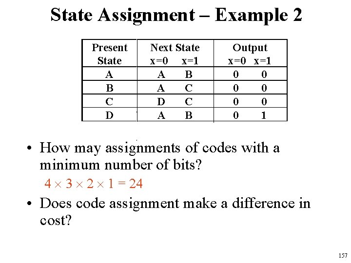
State Assignment – Example 2 Present State A B C D Next State x=0 x=1 A B A C D C A B Output x=0 x=1 0 0 0 0 1 • How may assignments of codes with a minimum number of bits? 4 3 2 1 = 24 • Does code assignment make a difference in cost? 157

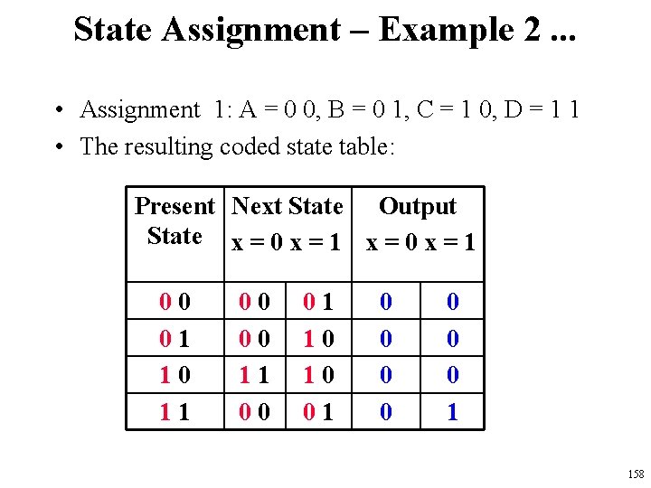
State Assignment – Example 2. . . • Assignment 1: A = 0 0, B = 0 1, C = 1 0, D = 1 1 • The resulting coded state table: Present Next State Output State x = 0 x = 1 00 01 10 11 00 01 10 10 01 0 0 0 0 1 158

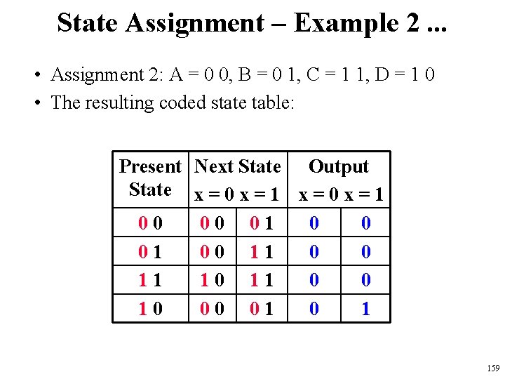
State Assignment – Example 2. . . • Assignment 2: A = 0 0, B = 0 1, C = 1 1, D = 1 0 • The resulting coded state table: Present Next State Output State x = 0 x = 1 00 00 01 00 11 0 0 11 10 11 0 0 10 00 01 0 1 159

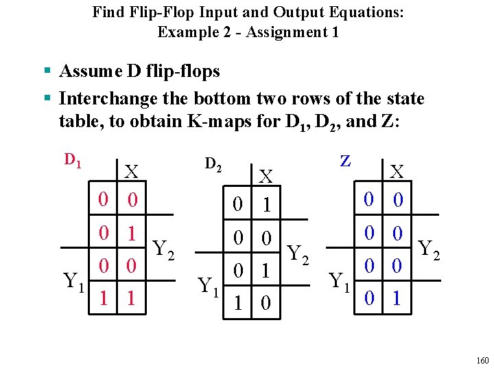
Find Flip-Flop Input and Output Equations: Example 2 - Assignment 1 § Assume D flip-flops § Interchange the bottom two rows of the state table, to obtain K-maps for D 1, D 2, and Z: D 1 X 0 0 0 1 Y 2 0 0 Y 1 1 1 D 2 X 0 1 Z X 0 0 0 Y 2 0 0 0 1 Y 1 0 160

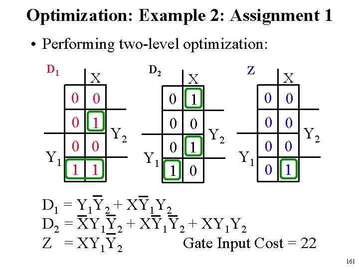
Optimization: Example 2: Assignment 1 • Performing two-level optimization: D 1 X 0 0 0 1 Y 2 0 0 Y 1 1 1 D 2 X 0 1 Z X 0 0 0 Y 2 0 0 0 1 Y 1 0 1 1 0 D 1 = Y 1 Y 2 + XY 1 Y 2 D 2 = XY 1 Y 2 + XY 1 Y 2 Z = XY 1 Y 2 Gate Input Cost = 22 161

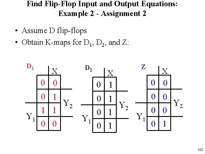
Find Flip-Flop Input and Output Equations: Example 2 - Assignment 2 • Assume D flip-flops • Obtain K-maps for D 1, D 2, and Z: D 1 X 0 0 0 1 Y 2 1 1 Y 1 0 0 D 2 X 0 1 Z X 0 0 0 1 Y 2 0 0 0 1 Y 1 0 1 162

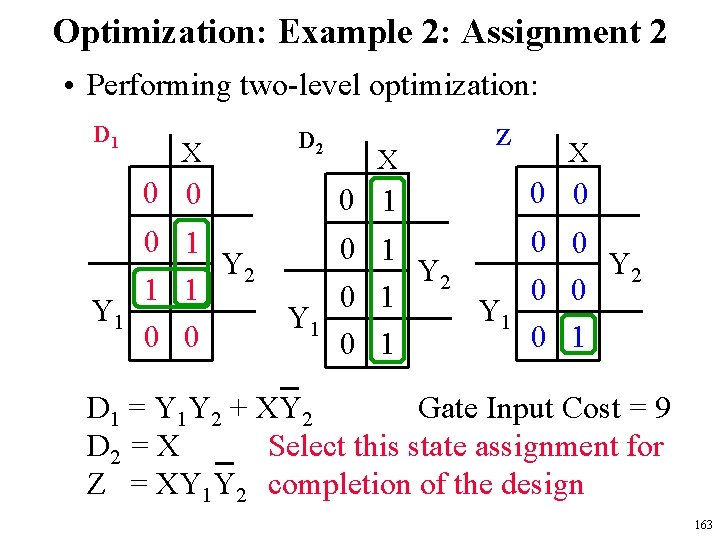
Optimization: Example 2: Assignment 2 • Performing two-level optimization: D 1 X 0 0 0 1 Y 2 1 1 Y 1 0 0 D 2 X 0 1 Z X 0 0 0 1 Y 2 0 0 0 1 Y 1 0 1 D 1 = Y 1 Y 2 + XY 2 Gate Input Cost = 9 D 2 = X Select this state assignment for Z = XY 1 Y 2 completion of the design 163

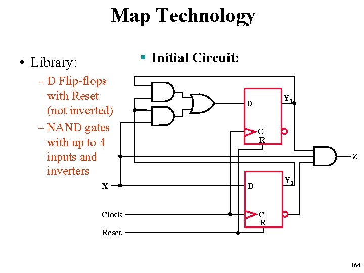
Map Technology § Initial Circuit: • Library: – D Flip-flops with Reset (not inverted) – NAND gates with up to 4 inputs and inverters X Clock Y 1 D C R Z Y 2 D C R Reset 164

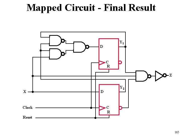
Mapped Circuit - Final Result Y 1 D C R Z X Clock Y 2 D C R Reset 165

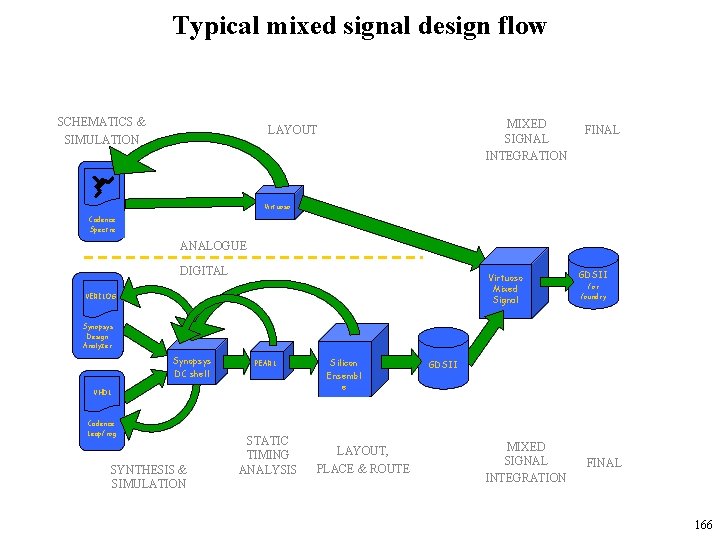
Typical mixed signal design flow SCHEMATICS & SIMULATION MIXED SIGNAL INTEGRATION LAYOUT FINAL Virtuoso Cadence Spectre ANALOGUE DIGITAL Virtuoso Mixed Signal VERILOG GDSII for foundry Synopsys Design Analyzer Synopsys DC shell PEARL VHDL Cadence Leapfrog SYNTHESIS & SIMULATION STATIC TIMING ANALYSIS Silicon Ensembl e LAYOUT, PLACE & ROUTE GDSII MIXED SIGNAL INTEGRATION FINAL 166

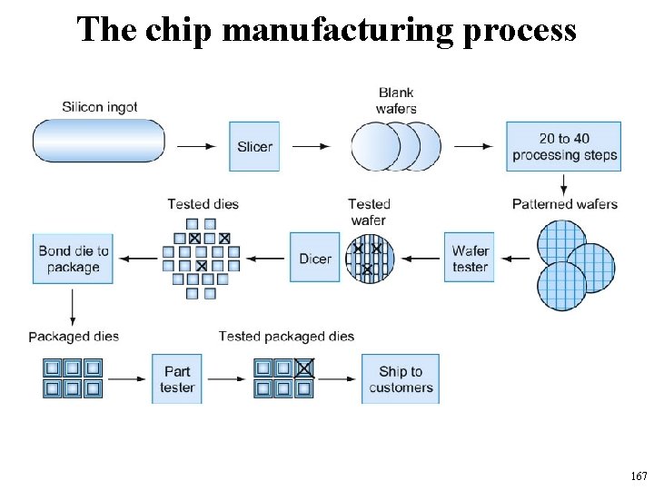
The chip manufacturing process 167

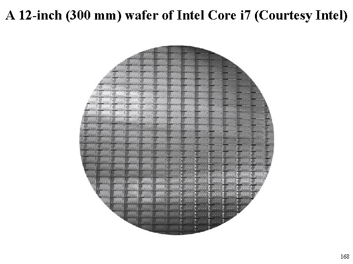
A 12 -inch (300 mm) wafer of Intel Core i 7 (Courtesy Intel) 168

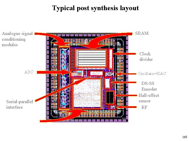
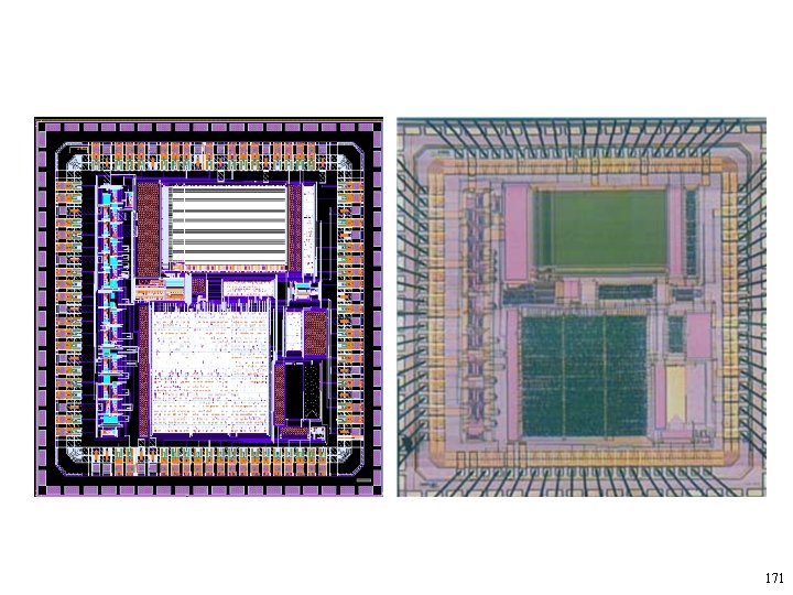
Typical post synthesis layout SRAM Analogue signal conditioning modules Clock divider ADC Oscillator+DAC DS-SS Encoder Hall-effect sensor RF Serial-parallel interface u. Processor 169

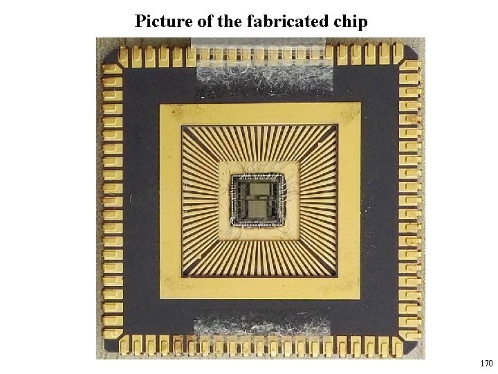
Picture of the fabricated chip 170

171

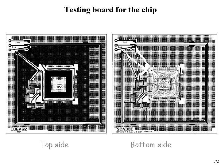
Testing board for the chip Top side Bottom side 172