Computer Architecture Prof Dr Nizamettin AYDIN naydinyildiz edu


- Slides: 77

Computer Architecture Prof. Dr. Nizamettin AYDIN naydin@yildiz. edu. tr nizamettinaydin@gmail. com http: //www. yildiz. edu. tr/~naydin 1

Memory Hierarchy 2

Outline • • Introduction Characteristics Memory hierarchy Cache Mapping function Replacement algorithms Write policy Examples 3

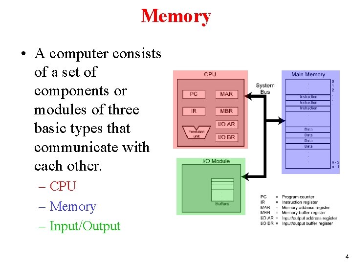
Memory • A computer consists of a set of components or modules of three basic types that communicate with each other. – CPU – Memory – Input/Output 4

Introduction • Memory lies at the heart of the storedprogram computer. • In this lecture, we focus on memory organization and architecture. • A clear understanding of these ideas is essential for the analysis of system performance. 5

Memory in a Modern Computer 6

Characteristics • • Location Capacity Unit of transfer Access method Performance Physical type Physical characteristics Organisation 7

Characteristics • Location • CPU is the reference – Internal – External • Capacity – Word size • The natural unit of organisation – Number of words • or Bytes 8

Characteristics • Unit of Transfer – Internal • Usually governed by data bus width – External • Usually a block which is much larger than a word – Addressable unit • Smallest location which can be uniquely addressed • Word internally • Cluster on disks 9

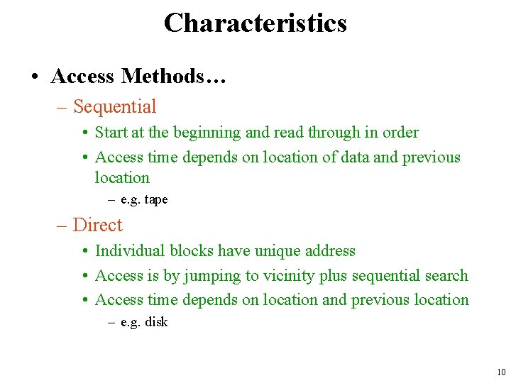
Characteristics • Access Methods… – Sequential • Start at the beginning and read through in order • Access time depends on location of data and previous location – e. g. tape – Direct • Individual blocks have unique address • Access is by jumping to vicinity plus sequential search • Access time depends on location and previous location – e. g. disk 10

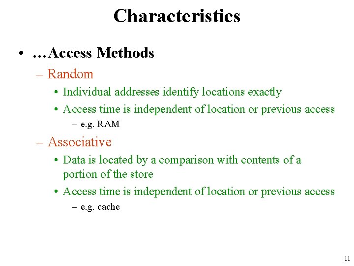
Characteristics • …Access Methods – Random • Individual addresses identify locations exactly • Access time is independent of location or previous access – e. g. RAM – Associative • Data is located by a comparison with contents of a portion of the store • Access time is independent of location or previous access – e. g. cache 11

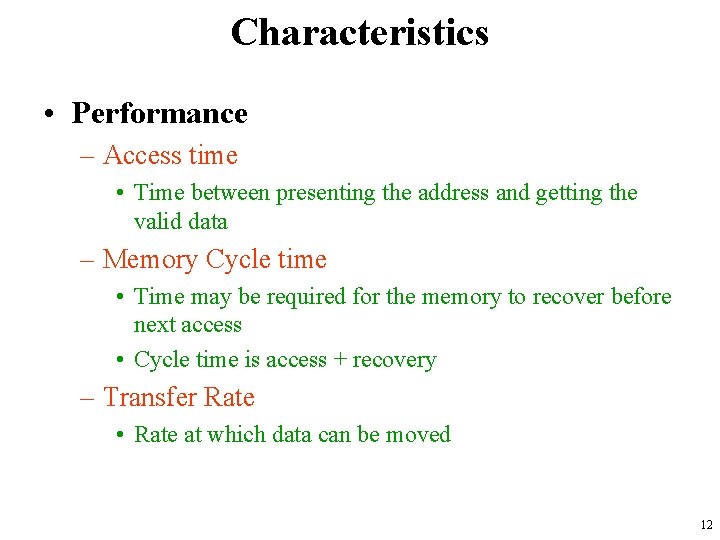
Characteristics • Performance – Access time • Time between presenting the address and getting the valid data – Memory Cycle time • Time may be required for the memory to recover before next access • Cycle time is access + recovery – Transfer Rate • Rate at which data can be moved 12

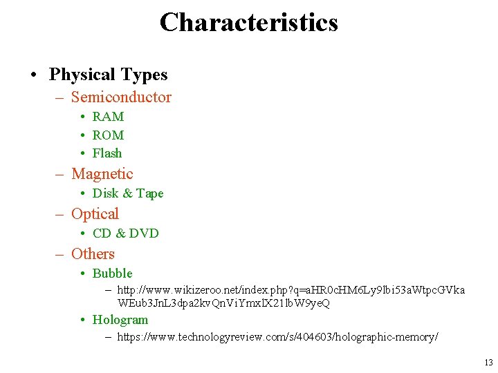
Characteristics • Physical Types – Semiconductor • RAM • ROM • Flash – Magnetic • Disk & Tape – Optical • CD & DVD – Others • Bubble – http: //www. wikizeroo. net/index. php? q=a. HR 0 c. HM 6 Ly 9 lbi 53 a. Wtpc. GVka WEub 3 Jn. L 3 dpa 2 kv. Qn. Vi. Ymxl. X 21 lb. W 9 ye. Q • Hologram – https: //www. technologyreview. com/s/404603/holographic-memory/ 13

Characteristics • Physical Characteristics – Decay – Volatility – Erasable – Power consumption • Organisation – Physical arrangement of bits into words – Not always obvious • e. g. interleaved 14

Characteristics • The Bottom Line – How much? • Capacity – How fast? • Time is money – How expensive? • So you want fast? – It is possible to build a computer which uses only static RAM • This would be very fast • This would need no cache • This would cost a very large amount 15

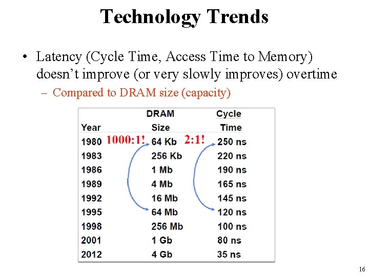
Technology Trends • Latency (Cycle Time, Access Time to Memory) doesn’t improve (or very slowly improves) overtime – Compared to DRAM size (capacity) 16

Processor-Memory Performance Gap 17

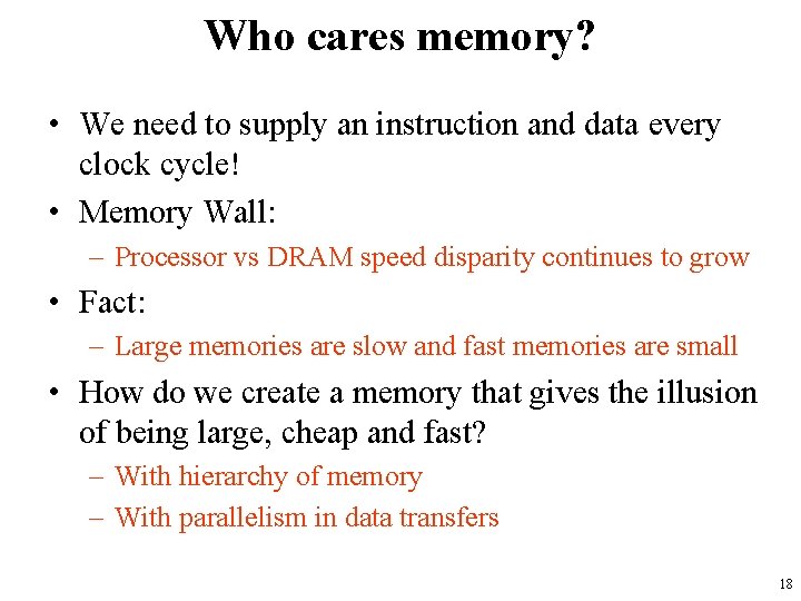
Who cares memory? • We need to supply an instruction and data every clock cycle! • Memory Wall: – Processor vs DRAM speed disparity continues to grow • Fact: – Large memories are slow and fast memories are small • How do we create a memory that gives the illusion of being large, cheap and fast? – With hierarchy of memory – With parallelism in data transfers 18

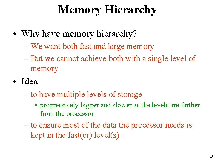
Memory Hierarchy • Why have memory hierarchy? – We want both fast and large memory – But we cannot achieve both with a single level of memory • Idea – to have multiple levels of storage • progressively bigger and slower as the levels are farther from the processor – to ensure most of the data the processor needs is kept in the fast(er) level(s) 19

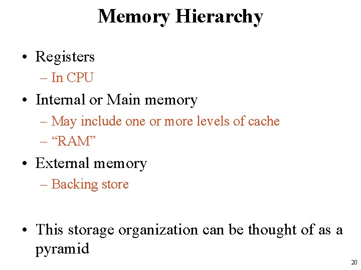
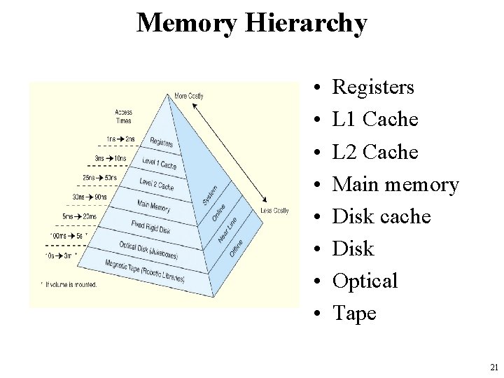
Memory Hierarchy • Registers – In CPU • Internal or Main memory – May include one or more levels of cache – “RAM” • External memory – Backing store • This storage organization can be thought of as a pyramid 20

Memory Hierarchy • • Registers L 1 Cache L 2 Cache Main memory Disk cache Disk Optical Tape 21

Cache • Stores data so that future requests for that data can be served faster – Cache hit: if the requested data is in the cache – Otherwise it is a cache miss • Two type of caches – Instruction cache – Data cache • Every general purpose computer built today includes caches • Completely managed by the hardware, transparent to the programmer 22

A Typical Memory Hierarchy • The principle of locality states that programs access a relatively small portion of the address space at any instant of time. 23

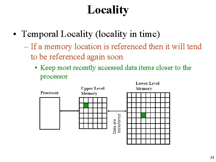
Locality • Temporal Locality (locality in time) – If a memory location is referenced then it will tend to be referenced again soon • Keep most recently accessed data items closer to the processor 24

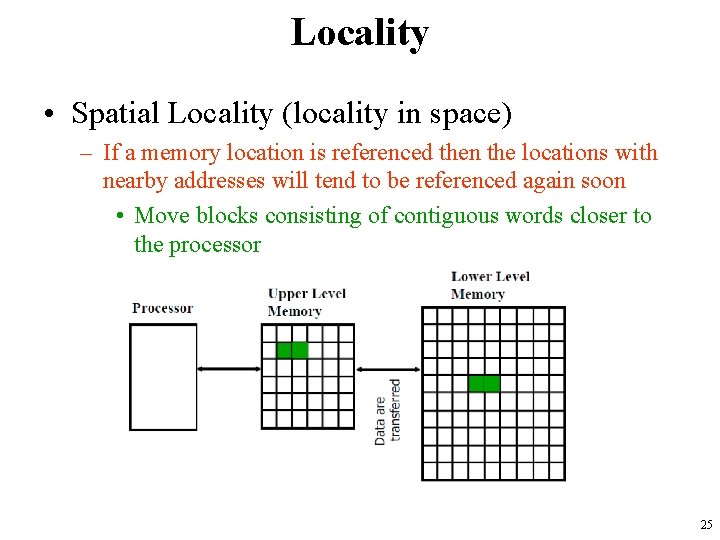
Locality • Spatial Locality (locality in space) – If a memory location is referenced then the locations with nearby addresses will tend to be referenced again soon • Move blocks consisting of contiguous words closer to the processor 25

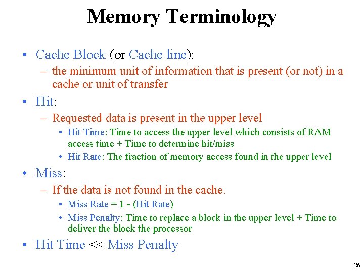
Memory Terminology • Cache Block (or Cache line): – the minimum unit of information that is present (or not) in a cache or unit of transfer • Hit: – Requested data is present in the upper level • Hit Time: Time to access the upper level which consists of RAM access time + Time to determine hit/miss • Hit Rate: The fraction of memory access found in the upper level • Miss: – If the data is not found in the cache. • Miss Rate = 1 - (Hit Rate) • Miss Penalty: Time to replace a block in the upper level + Time to deliver the block the processor • Hit Time << Miss Penalty 26

Memory Hierarchy- relative data size 27

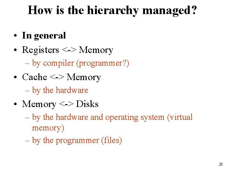
How is the hierarchy managed? • In general • Registers <-> Memory – by compiler (programmer? ) • Cache <-> Memory – by the hardware • Memory <-> Disks – by the hardware and operating system (virtual memory) – by the programmer (files) 28

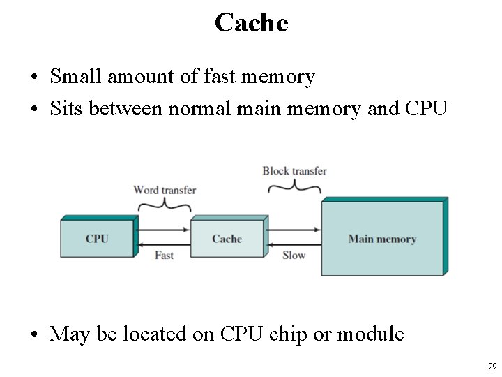
Cache • Small amount of fast memory • Sits between normal main memory and CPU • May be located on CPU chip or module 29

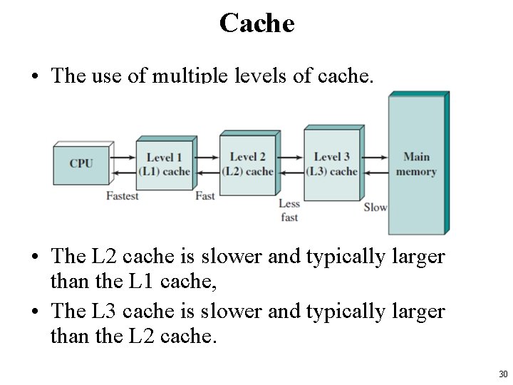
Cache • The use of multiple levels of cache. • The L 2 cache is slower and typically larger than the L 1 cache, • The L 3 cache is slower and typically larger than the L 2 cache. 30

Cache • The purpose of cache memory – to speed up accesses by storing recently used data closer to the CPU • It is much smaller than main memory • Its access time is a fraction of that of main memory. • main memory is accessed by address, • cache is typically accessed by content; – hence, it is often called content addressable memory. • Because of this, a single large cache memory isn’t always desirable – it takes longer to search. 31

Cache • The content that is addressed in content addressable cache memory is a subset of the bits of a main memory address called a field. – The fields into which a memory address is divided provide a many-to-one mapping between larger main memory and the smaller cache memory. • Many blocks of main memory map to a single block of cache. • A tag field in the cache block distinguishes one cached memory block from another. 32

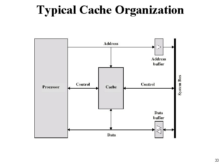
Typical Cache Organization 33

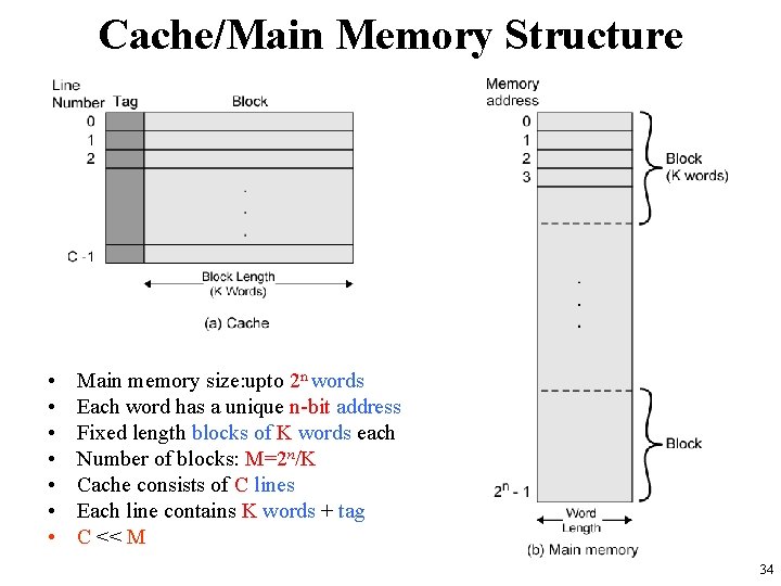
Cache/Main Memory Structure • • Main memory size: upto 2 n words Each word has a unique n-bit address Fixed length blocks of K words each Number of blocks: M=2 n/K Cache consists of C lines Each line contains K words + tag C << M 34

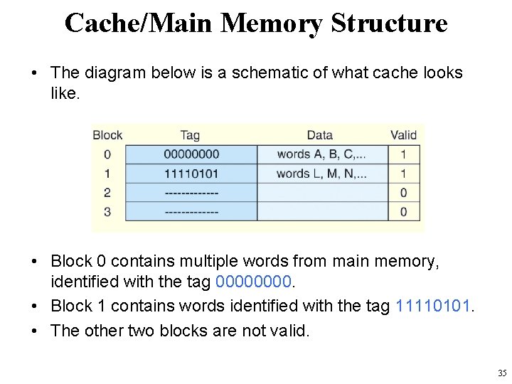
Cache/Main Memory Structure • The diagram below is a schematic of what cache looks like. • Block 0 contains multiple words from main memory, identified with the tag 0000. • Block 1 contains words identified with the tag 11110101. • The other two blocks are not valid. 35

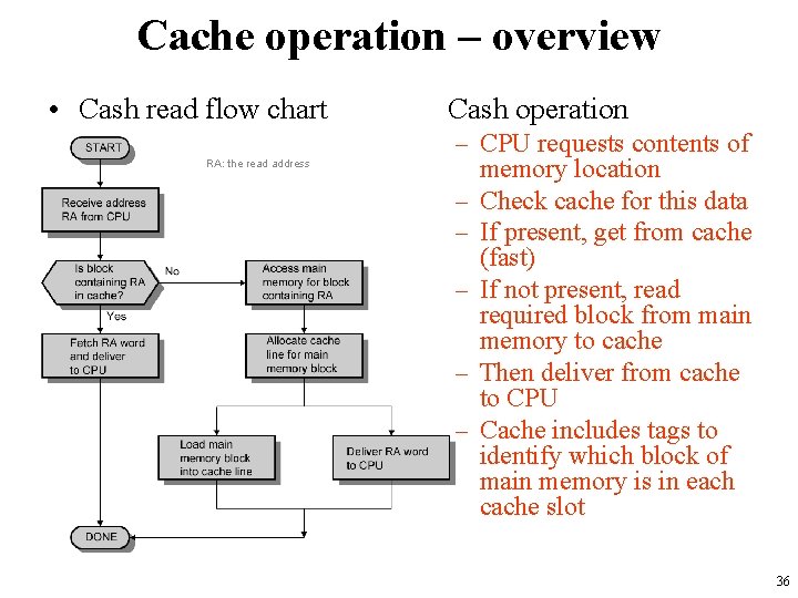
Cache operation – overview • Cash read flow chart RA: the read address Cash operation – CPU requests contents of memory location – Check cache for this data – If present, get from cache (fast) – If not present, read required block from main memory to cache – Then deliver from cache to CPU – Cache includes tags to identify which block of main memory is in each cache slot 36

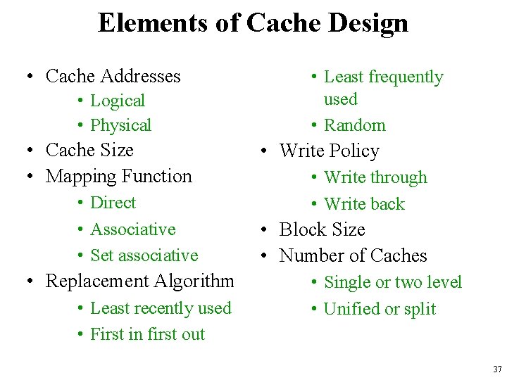
Elements of Cache Design • Cache Addresses • Logical • Physical • Cache Size • Mapping Function • Direct • Associative • Set associative • Replacement Algorithm • Least recently used • First in first out • Least frequently used • Random • Write Policy • Write through • Write back • Block Size • Number of Caches • Single or two level • Unified or split 37

Cache Addresses • Almost all nonembedded processors, and many embedded processors, support virtual Memory – a facility that allows programs to address memory from a logical point of view, without regard to the amount of main memory physically available. • When virtual memory is used, the address fields of machine instructions contain virtual addresses. • For reads to and writes from main memory, a hardware memory management unit (MMU) translates each virtual address into a physical address in main memory. 38

Cache Addresses • When virtual addresses are used, the system designer may choose to place the cache between the processor and the MMU or between the MMU and main memory. • A logical cache, also known as a virtual cache, stores data using virtual addresses. – The processor accesses the cache directly, without going through the MMU. • A physical cache stores data using main memory physical addresses. 39

Cache Addresses • • • cache access speed of the logical cache is faster than for a physical cache, because the cache can respond before the MMU performs an address translation. The disadvantage has to do with the fact that most virtual memory systems supply each application with the same virtual memory address space. That is, each application sees a virtual memory that starts at address 0. Thus, the same virtual address in two different applications refers to two different physical addresses. The cache memory must therefore be completely flushed with each application context switch, or extra bits must be added to each line of the cache to identify which virtual address space this address refers to. 40

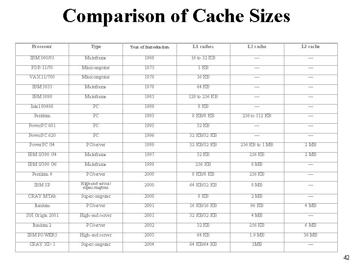
Cache Size does matter • We would like the size of the cache to be small enough so that the overall average cost per bit is close to that of main memory alone and large enough so that the overall average access time is close to that of the cache alone. • Cost – More cache is expensive • Speed – More cache is faster (up to a point) – Checking cache for data takes time 41

Comparison of Cache Sizes Processor Type Year of Introduction L 1 cachea L 2 cache L 3 cache IBM 360/85 Mainframe 1968 16 to 32 KB — — PDP-11/70 Minicomputer 1975 1 KB — — VAX 11/780 Minicomputer 1978 16 KB — — IBM 3033 Mainframe 1978 64 KB — — IBM 3090 Mainframe 1985 128 to 256 KB — — Intel 80486 PC 1989 8 KB — — Pentium PC 1993 8 KB/8 KB 256 to 512 KB — Power. PC 601 PC 1993 32 KB — — Power. PC 620 PC 1996 32 KB/32 KB — — Power. PC G 4 PC/server 1999 32 KB/32 KB 256 KB to 1 MB 2 MB IBM S/390 G 4 Mainframe 1997 32 KB 256 KB 2 MB IBM S/390 G 6 Mainframe 1999 256 KB 8 MB — Pentium 4 PC/server 2000 8 KB/8 KB 256 KB — IBM SP High-end server/ supercomputer 2000 64 KB/32 KB 8 MB — CRAY MTAb Supercomputer 2000 8 KB 2 MB — Itanium PC/server 2001 16 KB/16 KB 96 KB 4 MB SGI Origin 2001 High-end server 2001 32 KB/32 KB 4 MB — Itanium 2 PC/server 2002 32 KB 256 KB 6 MB IBM POWER 5 High-end server 2003 64 KB 1. 9 MB 36 MB CRAY XD-1 Supercomputer 2004 64 KB/64 KB 1 MB — 42

Mapping Function • Because there are fewer lines than main memory blocks, an algorithm is needed for mapping main memory blocks into cache lines. • Which main memory block currently occupies a cache line? • Three techniques can be used: – Direct mapping – Associative mapping – Set associative mapping 43

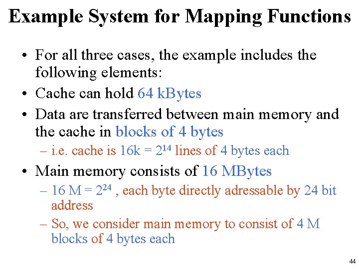
Example System for Mapping Functions • For all three cases, the example includes the following elements: • Cache can hold 64 k. Bytes • Data are transferred between main memory and the cache in blocks of 4 bytes – i. e. cache is 16 k = 214 lines of 4 bytes each • Main memory consists of 16 MBytes – 16 M = 224 , each byte directly adressable by 24 bit address – So, we consider main memory to consist of 4 M blocks of 4 bytes each 44

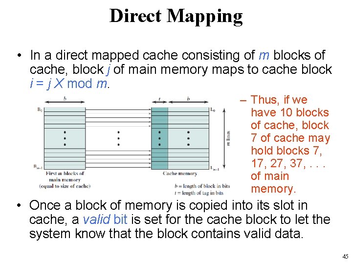
Direct Mapping • In a direct mapped cache consisting of m blocks of cache, block j of main memory maps to cache block i = j X mod m. – Thus, if we have 10 blocks of cache, block 7 of cache may hold blocks 7, 17, 27, 37, . . . of main memory. • Once a block of memory is copied into its slot in cache, a valid bit is set for the cache block to let the system know that the block contains valid data. 45

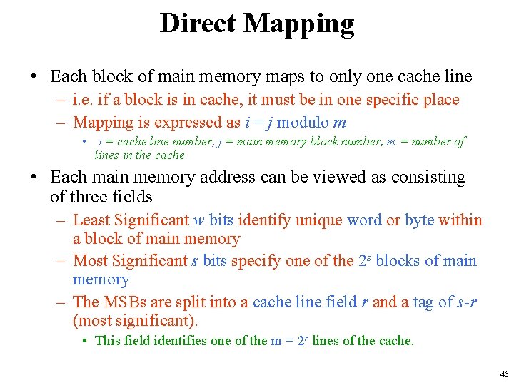
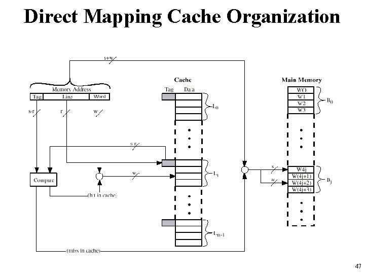
Direct Mapping • Each block of main memory maps to only one cache line – i. e. if a block is in cache, it must be in one specific place – Mapping is expressed as i = j modulo m • i = cache line number, j = main memory block number, m = number of lines in the cache • Each main memory address can be viewed as consisting of three fields – Least Significant w bits identify unique word or byte within a block of main memory – Most Significant s bits specify one of the 2 s blocks of main memory – The MSBs are split into a cache line field r and a tag of s-r (most significant). • This field identifies one of the m = 2 r lines of the cache. 46

Direct Mapping Cache Organization 47

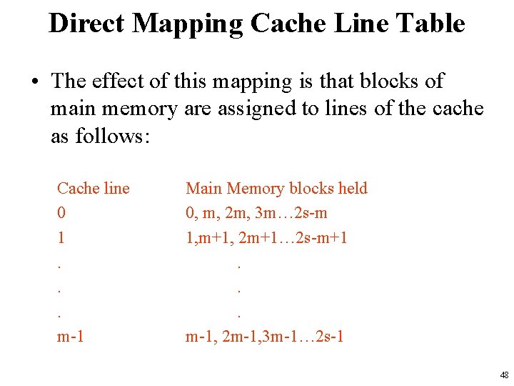
Direct Mapping Cache Line Table • The effect of this mapping is that blocks of main memory are assigned to lines of the cache as follows: Cache line 0 1. . . m-1 Main Memory blocks held 0, m, 2 m, 3 m… 2 s-m 1, m+1, 2 m+1… 2 s-m+1. . . m-1, 2 m-1, 3 m-1… 2 s-1 48

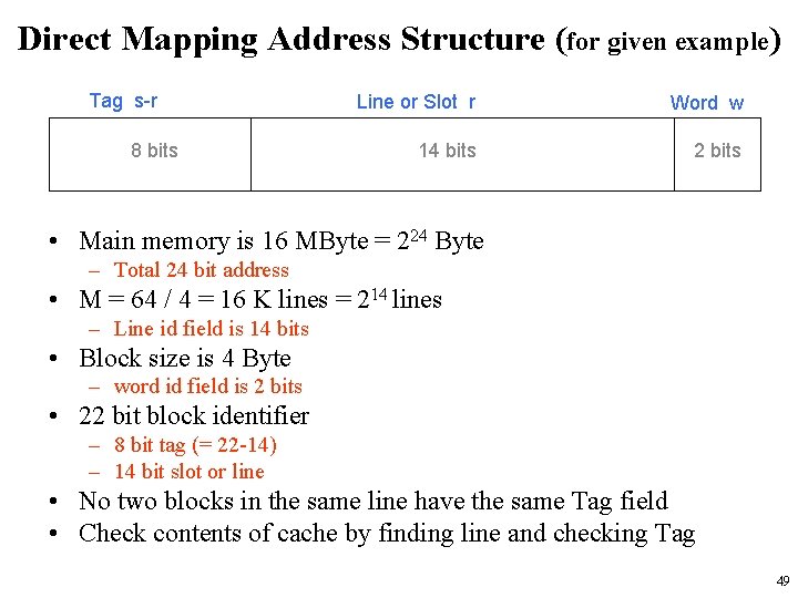
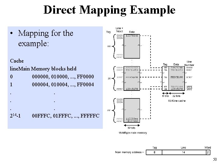
Direct Mapping Address Structure (for given example) Tag s-r 8 bits Line or Slot r Word w 14 bits 2 bits • Main memory is 16 MByte = 224 Byte – Total 24 bit address • M = 64 / 4 = 16 K lines = 214 lines – Line id field is 14 bits • Block size is 4 Byte – word id field is 2 bits • 22 bit block identifier – 8 bit tag (= 22 -14) – 14 bit slot or line • No two blocks in the same line have the same Tag field • Check contents of cache by finding line and checking Tag 49

Direct Mapping Example • Mapping for the example: Cache line. Main Memory blocks held 0 000000, 010000, . . . , FF 0000 1 000004, 010004, . . . , FF 0004. . . 214 -1 00 FFFC, 01 FFFC, . . . , FFFFFC 50

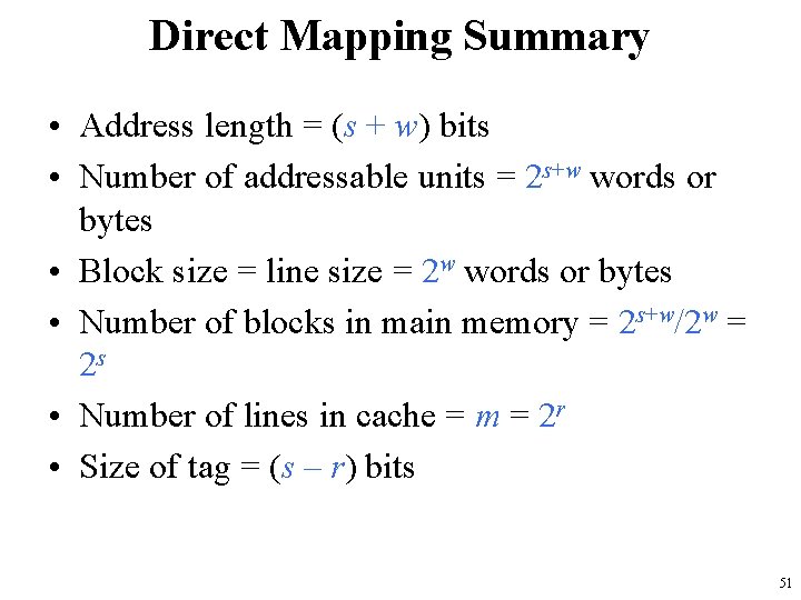
Direct Mapping Summary • Address length = (s + w) bits • Number of addressable units = 2 s+w words or bytes • Block size = line size = 2 w words or bytes • Number of blocks in main memory = 2 s+w/2 w = 2 s • Number of lines in cache = m = 2 r • Size of tag = (s – r) bits 51

Direct Mapping pros & cons • Simple • Inexpensive • Fixed location for given block – If a program accesses 2 blocks that map to the same line repeatedly, cache misses are very high 52

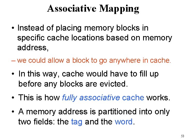
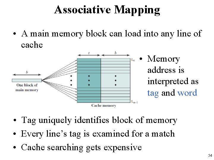
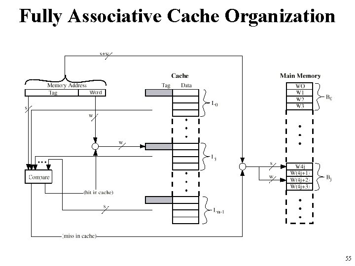
Associative Mapping • Instead of placing memory blocks in specific cache locations based on memory address, – we could allow a block to go anywhere in cache. • In this way, cache would have to fill up before any blocks are evicted. • This is how fully associative cache works. • A memory address is partitioned into only two fields: the tag and the word. 53

Associative Mapping • A main memory block can load into any line of cache • Memory address is interpreted as tag and word • Tag uniquely identifies block of memory • Every line’s tag is examined for a match • Cache searching gets expensive 54

Fully Associative Cache Organization 55

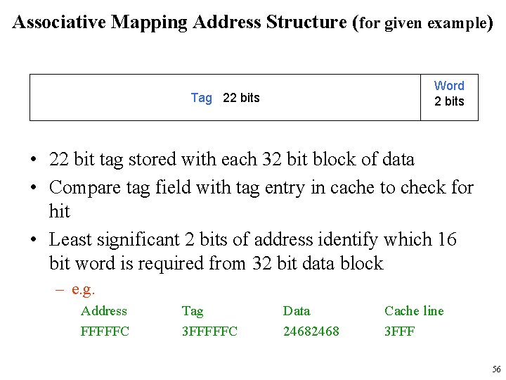
Associative Mapping Address Structure (for given example) Word 2 bits Tag 22 bits • 22 bit tag stored with each 32 bit block of data • Compare tag field with tag entry in cache to check for hit • Least significant 2 bits of address identify which 16 bit word is required from 32 bit data block – e. g. Address FFFFFC Tag 3 FFFFFC Data 2468 Cache line 3 FFF 56

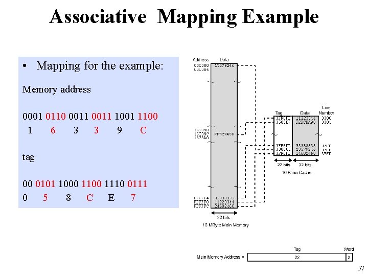
Associative Mapping Example • Mapping for the example: Memory address 0001 0110 0011 1001 1100 1 6 3 3 9 C tag 00 0101 1000 1110 0111 0 5 8 C E 7 57

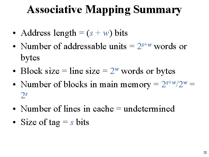
Associative Mapping Summary • Address length = (s + w) bits • Number of addressable units = 2 s+w words or bytes • Block size = line size = 2 w words or bytes • Number of blocks in main memory = 2 s+w/2 w = 2 s • Number of lines in cache = undetermined • Size of tag = s bits 58

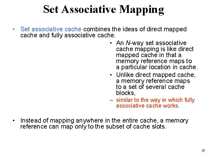
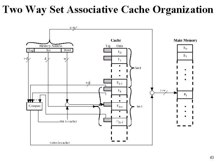
Set Associative Mapping • Set associative cache combines the ideas of direct mapped cache and fully associative cache. • An N-way set associative cache mapping is like direct mapped cache in that a memory reference maps to a particular location in cache. • Unlike direct mapped cache, a memory reference maps to a set of several cache blocks, – similar to the way in which fully associative cache works. • Instead of mapping anywhere in the entire cache, a memory reference can map only to the subset of cache slots. 59

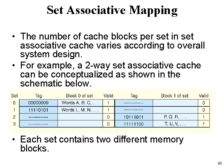
Set Associative Mapping • The number of cache blocks per set in set associative cache varies according to overall system design. • For example, a 2 -way set associative cache can be conceptualized as shown in the schematic below. • Each set contains two different memory blocks. 60

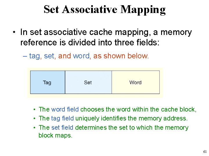
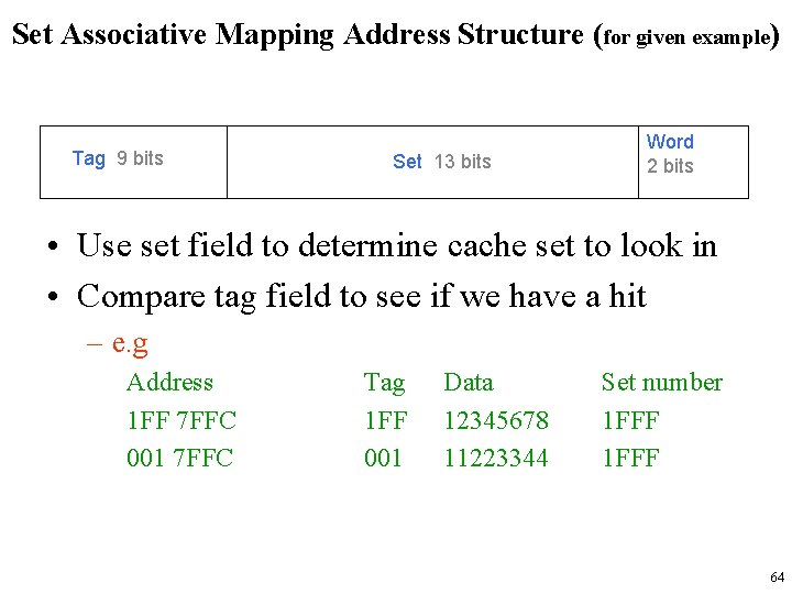
Set Associative Mapping • In set associative cache mapping, a memory reference is divided into three fields: – tag, set, and word, as shown below. • The word field chooses the word within the cache block, • The tag field uniquely identifies the memory address. • The set field determines the set to which the memory block maps. 61

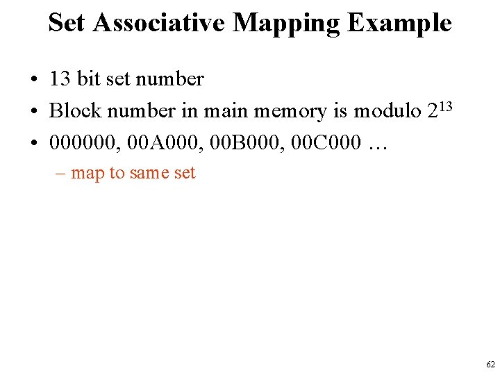
Set Associative Mapping Example • 13 bit set number • Block number in main memory is modulo 213 • 000000, 00 A 000, 00 B 000, 00 C 000 … – map to same set 62

Two Way Set Associative Cache Organization 63

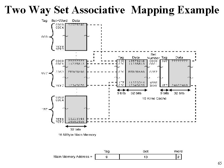
Set Associative Mapping Address Structure (for given example) Tag 9 bits Set 13 bits Word 2 bits • Use set field to determine cache set to look in • Compare tag field to see if we have a hit – e. g Address 1 FF 7 FFC 001 7 FFC Tag 1 FF 001 Data 12345678 11223344 Set number 1 FFF 64

Two Way Set Associative Mapping Example 65

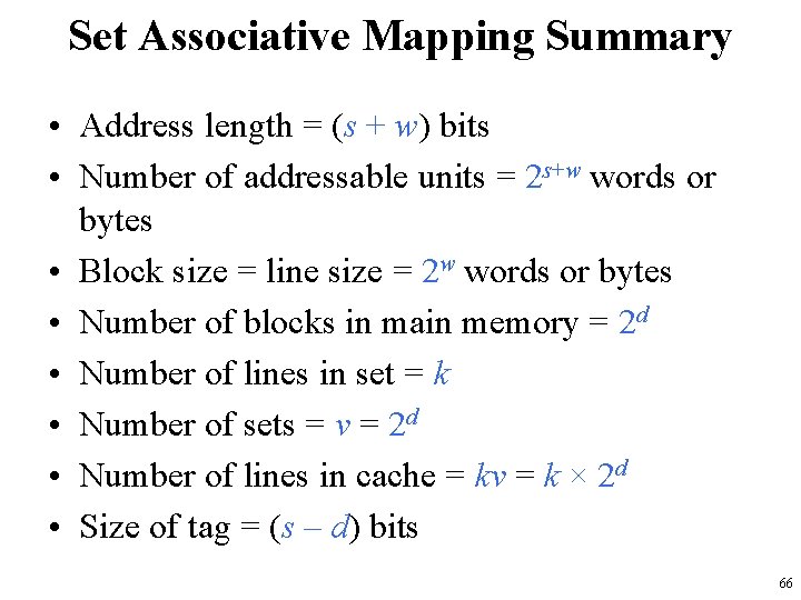
Set Associative Mapping Summary • Address length = (s + w) bits • Number of addressable units = 2 s+w words or bytes • Block size = line size = 2 w words or bytes • Number of blocks in main memory = 2 d • Number of lines in set = k • Number of sets = v = 2 d • Number of lines in cache = kv = k × 2 d • Size of tag = (s – d) bits 66

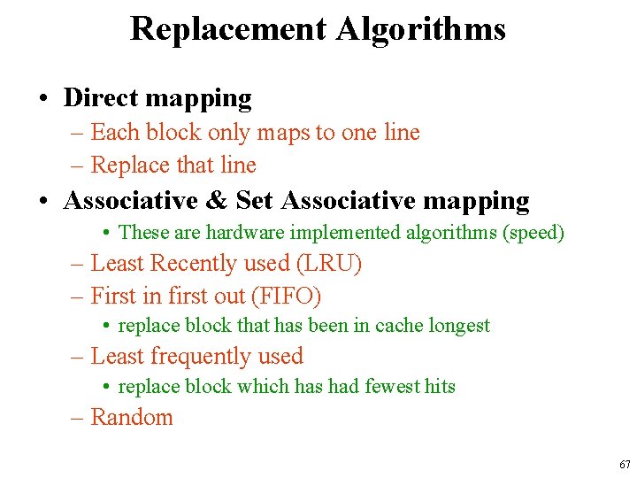
Replacement Algorithms • Direct mapping – Each block only maps to one line – Replace that line • Associative & Set Associative mapping • These are hardware implemented algorithms (speed) – Least Recently used (LRU) – First in first out (FIFO) • replace block that has been in cache longest – Least frequently used • replace block which has had fewest hits – Random 67

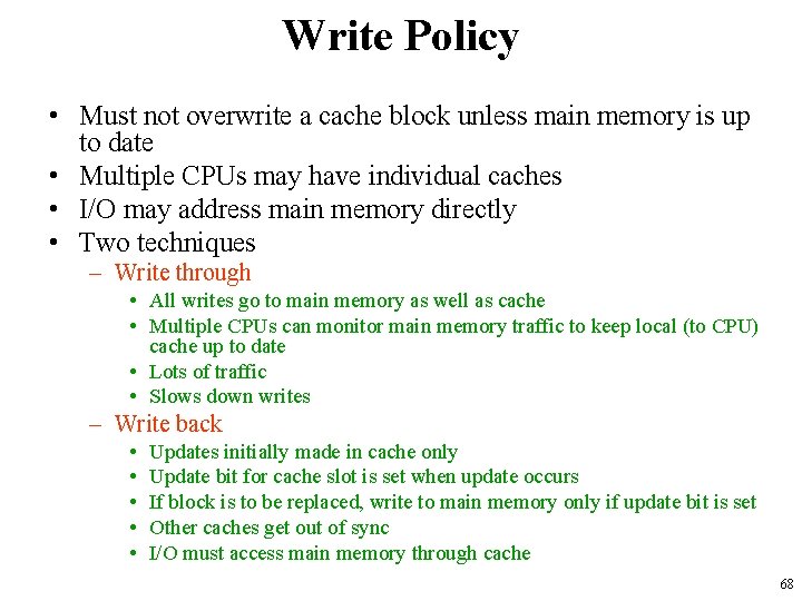
Write Policy • Must not overwrite a cache block unless main memory is up to date • Multiple CPUs may have individual caches • I/O may address main memory directly • Two techniques – Write through • All writes go to main memory as well as cache • Multiple CPUs can monitor main memory traffic to keep local (to CPU) cache up to date • Lots of traffic • Slows down writes – Write back • • • Updates initially made in cache only Update bit for cache slot is set when update occurs If block is to be replaced, write to main memory only if update bit is set Other caches get out of sync I/O must access main memory through cache 68

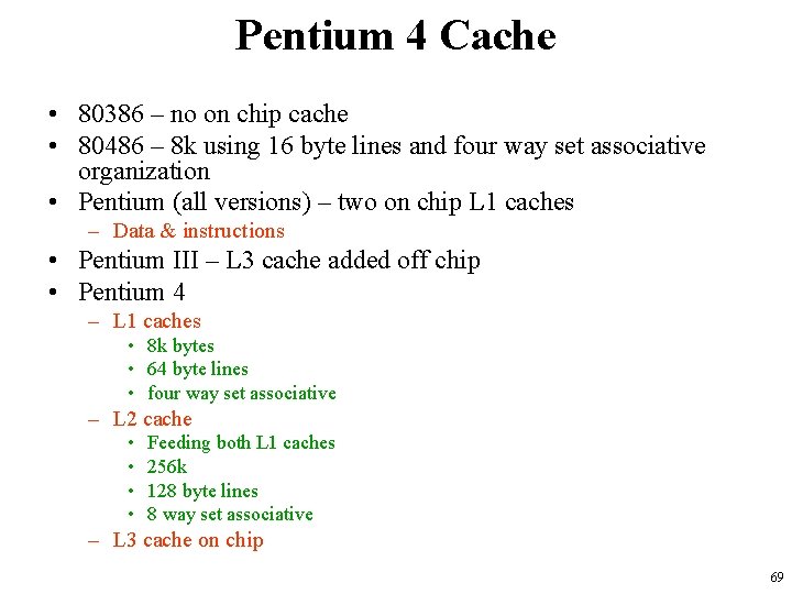
Pentium 4 Cache • 80386 – no on chip cache • 80486 – 8 k using 16 byte lines and four way set associative organization • Pentium (all versions) – two on chip L 1 caches – Data & instructions • Pentium III – L 3 cache added off chip • Pentium 4 – L 1 caches • 8 k bytes • 64 byte lines • four way set associative – L 2 cache • • Feeding both L 1 caches 256 k 128 byte lines 8 way set associative – L 3 cache on chip 69

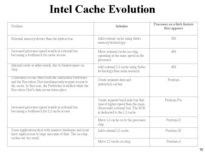
Intel Cache Evolution Problem Solution Processor on which feature first appears External memory slower than the system bus. Add external cache using faster memory technology. 386 Increased processor speed results in external bus becoming a bottleneck for cache access. Move external cache on-chip, operating at the same speed as the processor. 486 Add external L 2 cache using faster technology than main memory 486 Internal cache is rather small, due to limited space on chip Contention occurs when both the Instruction Prefetcher and the Execution Unit simultaneously require access to the cache. In that case, the Prefetcher is stalled while the Execution Unit’s data access takes place. Increased processor speed results in external bus becoming a bottleneck for L 2 cache access. Some applications deal with massive databases and must have rapid access to large amounts of data. The on-chip caches are too small. Create separate data and instruction caches. Pentium Create separate back-side bus that runs at higher speed than the main (front-side) external bus. The BSB is dedicated to the L 2 cache. Pentium Pro Move L 2 cache on to the processor chip. Pentium II Add external L 3 cache. Pentium III Move L 3 cache on-chip. Pentium 4 70

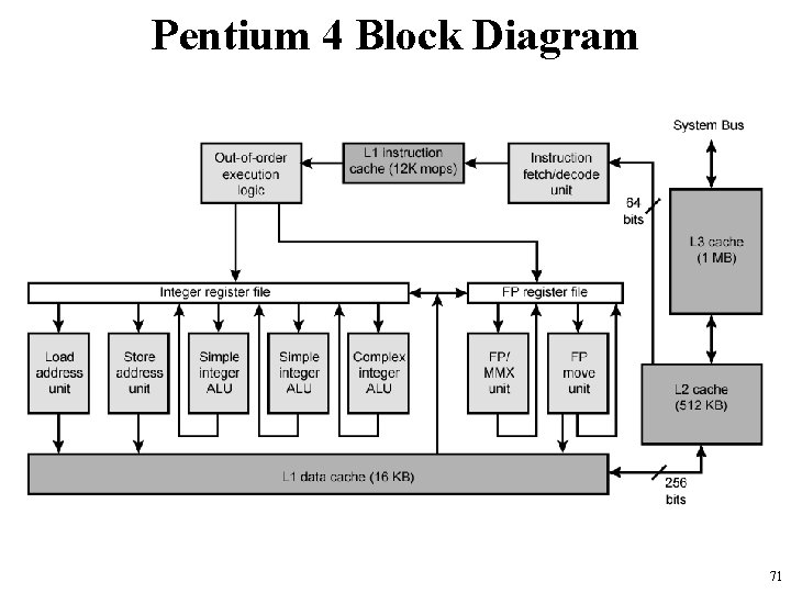
Pentium 4 Block Diagram 71

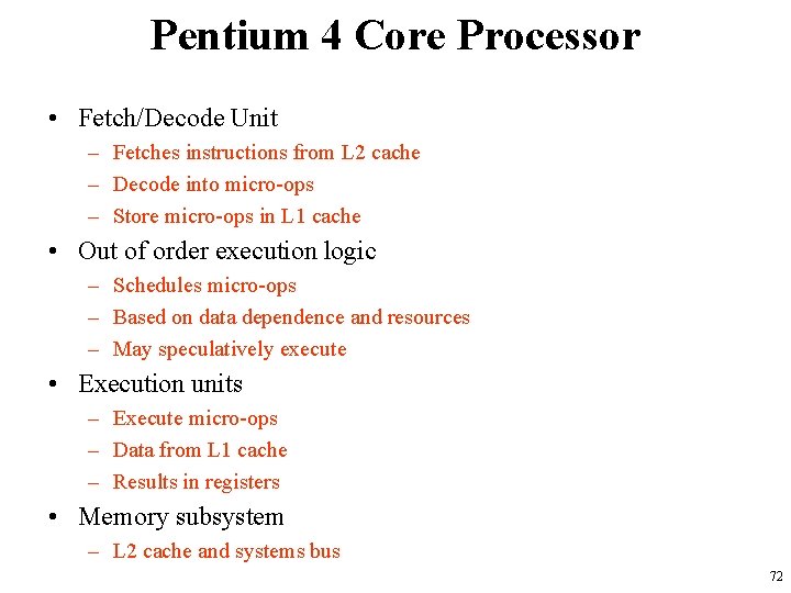
Pentium 4 Core Processor • Fetch/Decode Unit – Fetches instructions from L 2 cache – Decode into micro-ops – Store micro-ops in L 1 cache • Out of order execution logic – Schedules micro-ops – Based on data dependence and resources – May speculatively execute • Execution units – Execute micro-ops – Data from L 1 cache – Results in registers • Memory subsystem – L 2 cache and systems bus 72

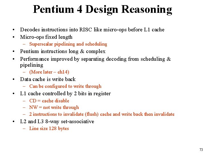
Pentium 4 Design Reasoning • Decodes instructions into RISC like micro-ops before L 1 cache • Micro-ops fixed length – Superscalar pipelining and scheduling • Pentium instructions long & complex • Performance improved by separating decoding from scheduling & pipelining – (More later – ch 14) • Data cache is write back – Can be configured to write through • L 1 cache controlled by 2 bits in register – CD = cache disable – NW = not write through – 2 instructions to invalidate (flush) cache and write back then invalidate • L 2 and L 3 8 -way set-associative – Line size 128 bytes 73

Power. PC Cache Organization • • • 601 – single 32 kb 8 way set associative 603 – 16 kb (2 x 8 kb) two way set associative 604 – 32 kb 620 – 64 kb G 3 & G 4 – 64 kb L 1 cache • 8 way set associative – 256 k, 512 k or 1 M L 2 cache • two way set associative • G 5 – 32 k. B instruction cache – 64 k. B data cache 74

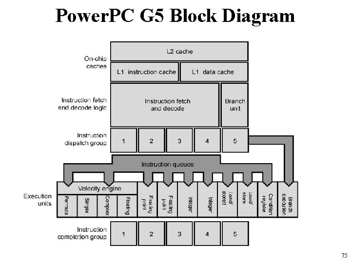
Power. PC G 5 Block Diagram 75

Internet Sources • Manufacturer sites – Intel – IBM – Motorola • Search on cache 76

77