Computer Architecture Processor Design Veton Kpuska Chapter Outline
![Abstract and Concrete RTN for SRC: add Instruction Abstract RTN: (IR ← M[PC]: PC Abstract and Concrete RTN for SRC: add Instruction Abstract RTN: (IR ← M[PC]: PC](https://slidetodoc.com/presentation_image/442c20e15053160a6f4c17b6711db3fa/image-9.jpg)
![Control Sequence for the SRC add (: = op = 12) ® R[ra] ¬ Control Sequence for the SRC add (: = op = 12) ® R[ra] ¬](https://slidetodoc.com/presentation_image/442c20e15053160a6f4c17b6711db3fa/image-33.jpg)
![Control Sequence for the SRC addi (: = op= 13) ® R[ra] ¬ R[rb] Control Sequence for the SRC addi (: = op= 13) ® R[ra] ¬ R[rb]](https://slidetodoc.com/presentation_image/442c20e15053160a6f4c17b6711db3fa/image-34.jpg)
![Control Sequence for the SRC st st (: = op = 3) ® M[disp] Control Sequence for the SRC st st (: = op = 3) ® M[disp]](https://slidetodoc.com/presentation_image/442c20e15053160a6f4c17b6711db3fa/image-35.jpg)
![Control Sequence for the SRC ld ld (: = op = 1) ® R[ra] Control Sequence for the SRC ld ld (: = op = 1) ® R[ra]](https://slidetodoc.com/presentation_image/442c20e15053160a6f4c17b6711db3fa/image-36.jpg)
- Slides: 84

Computer Architecture Processor Design Veton Këpuska

Chapter Outline u u u u The Design Process A 1 -Bus Microarchitecture for the SRC Data Path Implementation Logic Design for the 1 -Bus SRC The Control Unit The 2 - and 3 -Bus Processor Designs The Machine Reset Machine Exceptions 11/2/2020 Veton Këpuska 2

The Design Process u Focus from RTN machine description to computer system design: n n u u Design of the central processing unit Logic designer’s point of view RTN and logic design tools presented in Chapter 2 will be used extensively. Goal is not simply to present a design of SRC but also to do the design in the way a designer would approach it. 11/2/2020 Veton Këpuska 3

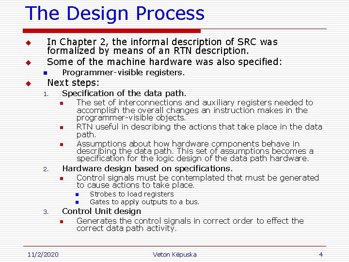
The Design Process u u In Chapter 2, the informal description of SRC was formalized by means of an RTN description. Some of the machine hardware was also specified: n u Programmer-visible registers. Next steps: 1. Specification of the data path. n n n 2. The set of interconnections and auxiliary registers needed to accomplish the overall changes an instruction makes in the programmer-visible objects. RTN useful in describing the actions that take place in the data path. Assumptions about how hardware components behave in describing the data path. This set of assumptions becomes a specification for the logic design of the data path hardware. Hardware design based on specifications. n Control signals must be contemplated that must be generated to cause actions to take place. n n 3. Control Unit design n 11/2/2020 Strobes to load registers Gates to apply outputs to a bus. Generates the control signals in correct order to effect the correct data path activity. Veton Këpuska 4

Abstract and Concrete Register Transfer Descriptions u u u The abstract RTN for SRC in Chapter 2 defines “what, ” not “how” A concrete RTN uses a specific set of real registers and buses to accomplish the effect of an abstract RTN statement Same abstract RTNs that implement the same ISA could have different concrete RTNs. 11/2/2020 Veton Këpuska 5

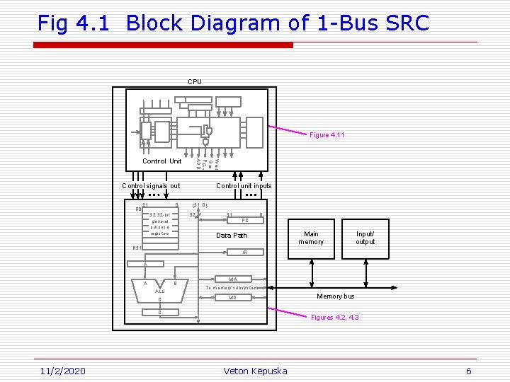
Fig 4. 1 Block Diagram of 1 -Bus SRC CPU Figure 4. 11 Wait Gra PCin ADD Control Unit Control signals out R 0 31 0 32 32 -bit general purpose registers Control unit inputs á 31. . 0ñ 32 31 0 PC Data Path R 31 Main memory Input/ output IR A A B ALU C MA To memory subsystem MD C 11/2/2020 Memory bus Figures 4. 2, 4. 3 Veton Këpuska 6

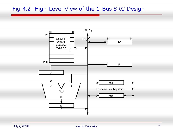
Fig 4. 2 High-Level View of the 1 -Bus SRC Design 31 0 á 31. . 0ñ R 0 32 32 -bit general purpose registers 31 32 0 PC R 31 IR A A MA B ALU To memory subsystem MD C C 11/2/2020 Veton Këpuska 7

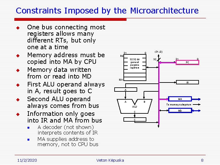
Constraints Imposed by the Microarchitecture u u u One bus connecting most registers allows many different RTs, but only one at a time Memory address must be copied into MA by CPU Memory data written from or read into MD First ALU operand always in A, result goes to C Second ALU operand always comes from bus Information only goes into IR and MA from bus n n 11/2/2020 31 0 á 31. . 0ñ R 0 32 32 -bit general purpose registers 32 31 0 PC R 31 IR A A B ALU C MA To memory subsystem MD C A decoder (not shown) interprets contents of IR MA supplies address to memory, not to CPU bus Veton Këpuska 8
![Abstract and Concrete RTN for SRC add Instruction Abstract RTN IR MPC PC Abstract and Concrete RTN for SRC: add Instruction Abstract RTN: (IR ← M[PC]: PC](https://slidetodoc.com/presentation_image/442c20e15053160a6f4c17b6711db3fa/image-9.jpg)
Abstract and Concrete RTN for SRC: add Instruction Abstract RTN: (IR ← M[PC]: PC ← PC + 4; instruction_execution); instruction_execution : = ( • • • add (: = op= 12) → R[ra] ← R[rb] + R[rc]: Tbl 4. 1 Concrete RTN for the add Instruction Step RTN T 0 MA ¬ PC: C ¬ PC + 4; T 1 MD ¬ M[MA]: PC ¬ C; T 2 IR ¬ MD; IF T 3 A ¬ R[rb]; IEx. T 4 C ¬ A + R[rc]; T 5 R[ra] ¬ C; 31 0 32 32 -bit general purpose registers u Parts of 2 RTs (IR ¬ M[PC]: PC ¬ PC + 4; ) done in T 0 Single add RT takes 3 concrete RTs (T 3, T 4, T 5) 11/2/2020 Veton Këpuska 32 31 0 PC R 31 IR A A B ALU C u á 31. . 0ñ R 0 MA To memory subsystem MD C 9

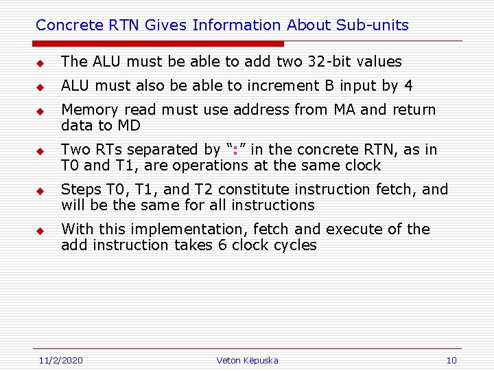
Concrete RTN Gives Information About Sub-units u The ALU must be able to add two 32 -bit values u ALU must also be able to increment B input by 4 u u Memory read must use address from MA and return data to MD Two RTs separated by “: ” in the concrete RTN, as in T 0 and T 1, are operations at the same clock Steps T 0, T 1, and T 2 constitute instruction fetch, and will be the same for all instructions With this implementation, fetch and execute of the add instruction takes 6 clock cycles 11/2/2020 Veton Këpuska 10

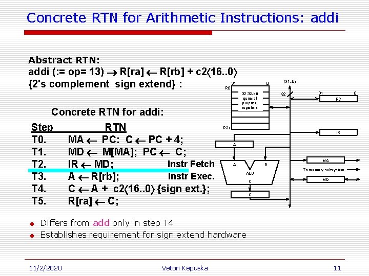
Concrete RTN for Arithmetic Instructions: addi Abstract RTN: addi (: = op= 13) ® R[ra] ¬ R[rb] + c 2á 16. . 0ñ {2's complement sign extend} : 31 0 á 31. . 0ñ R 0 32 32 -bit general purpose registers Concrete RTN for addi: Step T 0. T 1. T 2. T 3. T 4. T 5. u u RTN MA ¬ PC: C ¬ PC + 4; MD ¬ M[MA]; PC ¬ C; Instr Fetch IR ¬ MD; Instr Exec. A ¬ R[rb]; C ¬ A + c 2á 16. . 0ñ {sign ext. }; R[ra] ¬ C; 32 31 0 PC R 31 IR A A B ALU C MA To memory subsystem MD C Differs from add only in step T 4 Establishes requirement for sign extend hardware 11/2/2020 Veton Këpuska 11

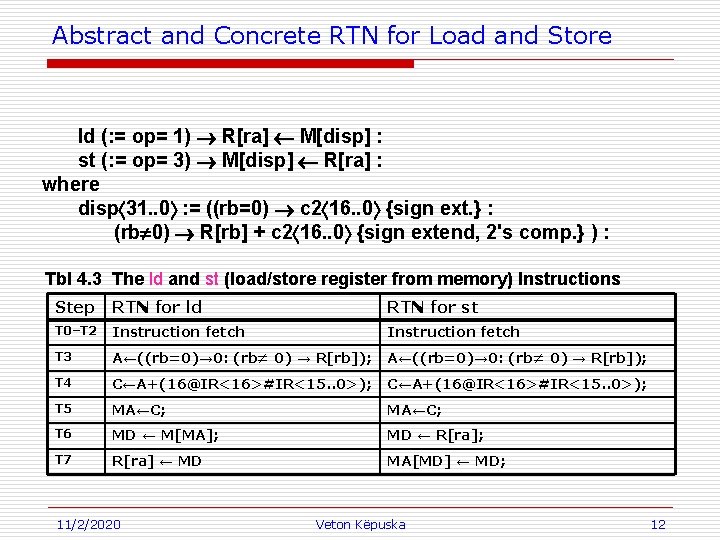
Abstract and Concrete RTN for Load and Store ld (: = op= 1) ® R[ra] ¬ M[disp] : st (: = op= 3) ® M[disp] ¬ R[ra] : where dispá 31. . 0ñ : = ((rb=0) ® c 2á 16. . 0ñ {sign ext. } : (rb¹ 0) ® R[rb] + c 2á 16. . 0ñ {sign extend, 2's comp. } ) : Tbl 4. 3 The ld and st (load/store register from memory) Instructions Step RTN for ld RTN for st T 0–T 2 Instruction fetch T 3 A←((rb=0)→ 0: (rb≠ 0) → R[rb]); T 4 C←A+(16@IR<16>#IR<15. . 0>); T 5 MA←C; T 6 MD ← M[MA]; MD ← R[ra]; T 7 R[ra] ← MD MA[MD] ← MD; 11/2/2020 Veton Këpuska 12

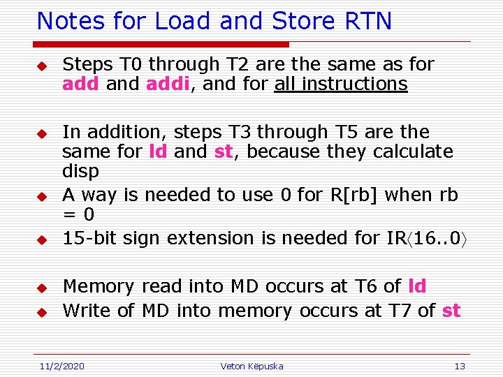
Notes for Load and Store RTN u u u Steps T 0 through T 2 are the same as for add and addi, and for all instructions In addition, steps T 3 through T 5 are the same for ld and st, because they calculate disp A way is needed to use 0 for R[rb] when rb =0 15 -bit sign extension is needed for IRá 16. . 0ñ Memory read into MD occurs at T 6 of ld Write of MD into memory occurs at T 7 of st 11/2/2020 Veton Këpuska 13

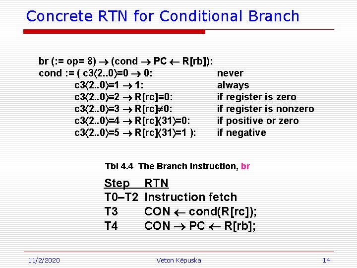
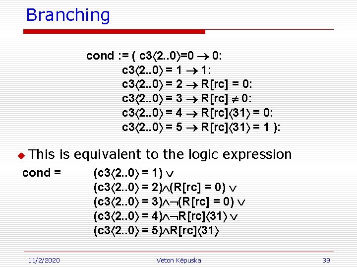
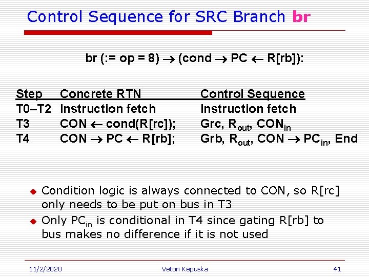
Concrete RTN for Conditional Branch br (: = op= 8) ® (cond ® PC ¬ R[rb]): cond : = ( c 3á 2. . 0ñ=0 ® 0: c 3á 2. . 0ñ=1 ® 1: c 3á 2. . 0ñ=2 ® R[rc]=0: c 3á 2. . 0ñ=3 ® R[rc]¹ 0: c 3á 2. . 0ñ=4 ® R[rc]á 31ñ=0: c 3á 2. . 0ñ=5 ® R[rc]á 31ñ=1 ): never always if register is zero if register is nonzero if positive or zero if negative Tbl 4. 4 The Branch Instruction, br Step T 0–T 2 T 3 T 4 11/2/2020 RTN Instruction fetch CON ¬ cond(R[rc]); CON ® PC ¬ R[rb]; Veton Këpuska 14

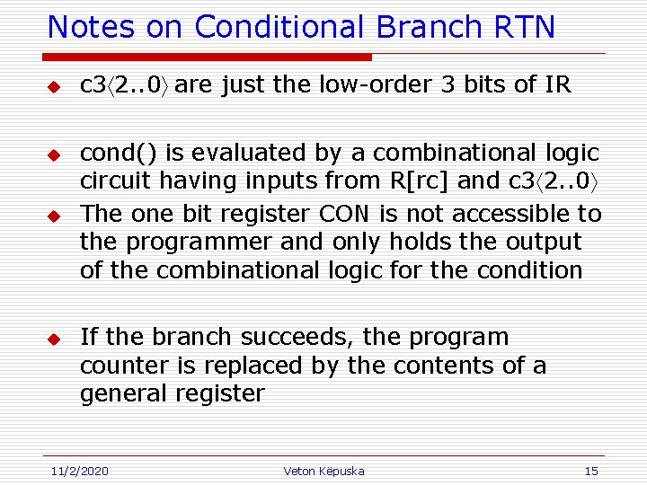
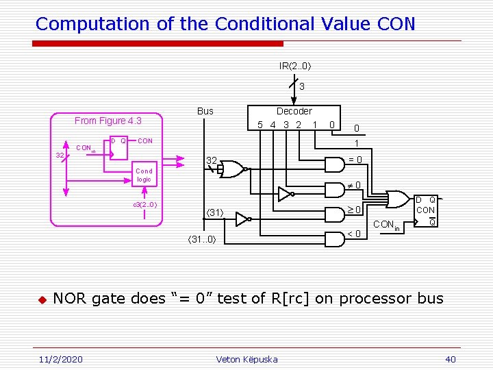
Notes on Conditional Branch RTN u u c 3á 2. . 0ñ are just the low-order 3 bits of IR cond() is evaluated by a combinational logic circuit having inputs from R[rc] and c 3á 2. . 0ñ The one bit register CON is not accessible to the programmer and only holds the output of the combinational logic for the condition If the branch succeeds, the program counter is replaced by the contents of a general register 11/2/2020 Veton Këpuska 15

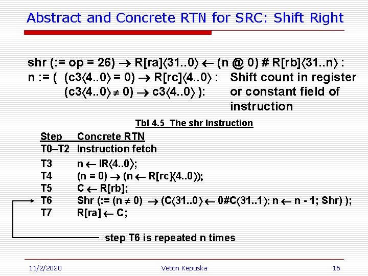
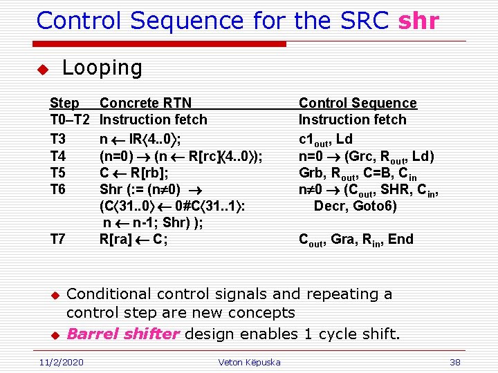
Abstract and Concrete RTN for SRC: Shift Right shr (: = op = 26) ® R[ra]á 31. . 0ñ ¬ (n @ 0) # R[rb]á 31. . nñ : n : = ( (c 3á 4. . 0ñ = 0) ® R[rc]á 4. . 0ñ : Shift count in register (c 3á 4. . 0ñ ¹ 0) ® c 3á 4. . 0ñ ): or constant field of instruction Tbl 4. 5 The shr Instruction Step T 0–T 2 T 3 T 4 T 5 T 6 T 7 Concrete RTN Instruction fetch n ¬ IRá 4. . 0ñ; (n = 0) ® (n ¬ R[rc]á 4. . 0 ñ); C ¬ R[rb]; Shr (: = (n ¹ 0) ® (Cá 31. . 0 ñ ¬ 0#Cá 31. . 1 ñ: n ¬ n - 1; Shr) ); R[ra] ¬ C; step T 6 is repeated n times 11/2/2020 Veton Këpuska 16

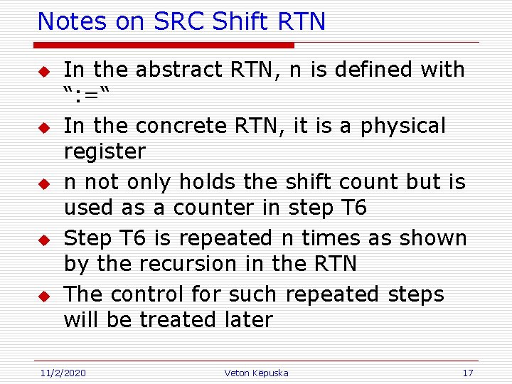
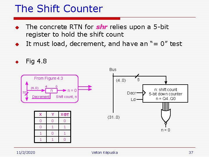
Notes on SRC Shift RTN u u u In the abstract RTN, n is defined with “: =“ In the concrete RTN, it is a physical register n not only holds the shift count but is used as a counter in step T 6 Step T 6 is repeated n times as shown by the recursion in the RTN The control for such repeated steps will be treated later 11/2/2020 Veton Këpuska 17

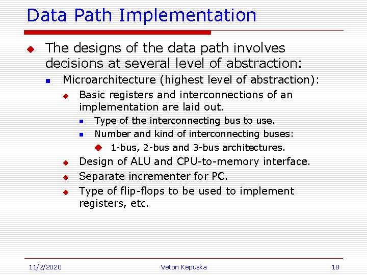
Data Path Implementation u The designs of the data path involves decisions at several level of abstraction: n Microarchitecture (highest level of abstraction): u Basic registers and interconnections of an implementation are laid out. n n u u u 11/2/2020 Type of the interconnecting bus to use. Number and kind of interconnecting buses: u 1 -bus, 2 -bus and 3 -bus architectures. Design of ALU and CPU-to-memory interface. Separate incrementer for PC. Type of flip-flops to be used to implement registers, etc. Veton Këpuska 18

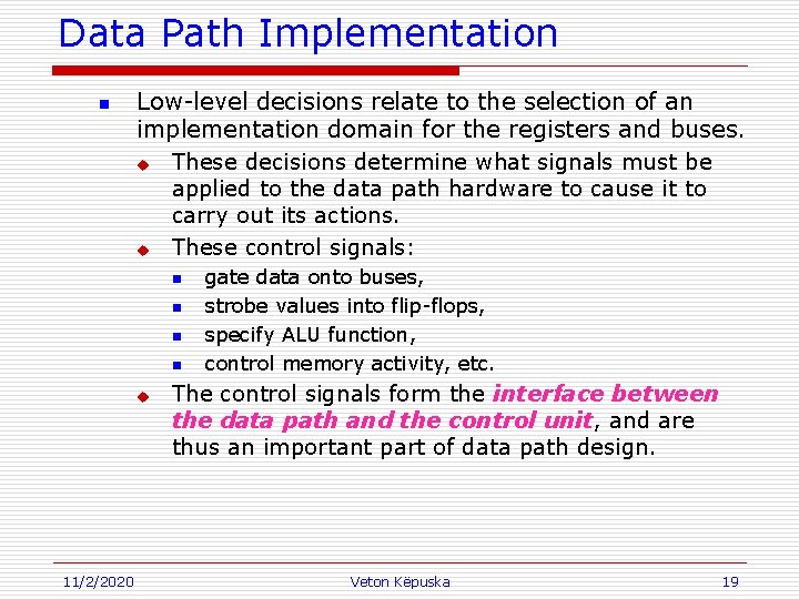
Data Path Implementation n Low-level decisions relate to the selection of an implementation domain for the registers and buses. u These decisions determine what signals must be applied to the data path hardware to cause it to carry out its actions. u These control signals: n n u 11/2/2020 gate data onto buses, strobe values into flip-flops, specify ALU function, control memory activity, etc. The control signals form the interface between the data path and the control unit, and are thus an important part of data path design. Veton Këpuska 19

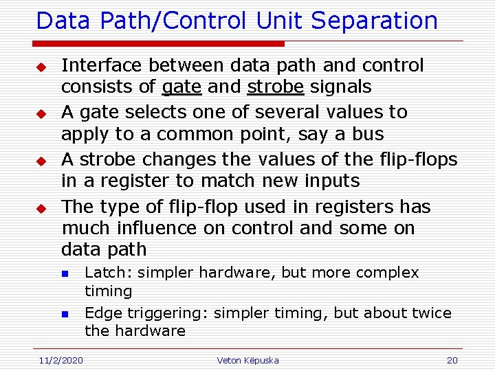
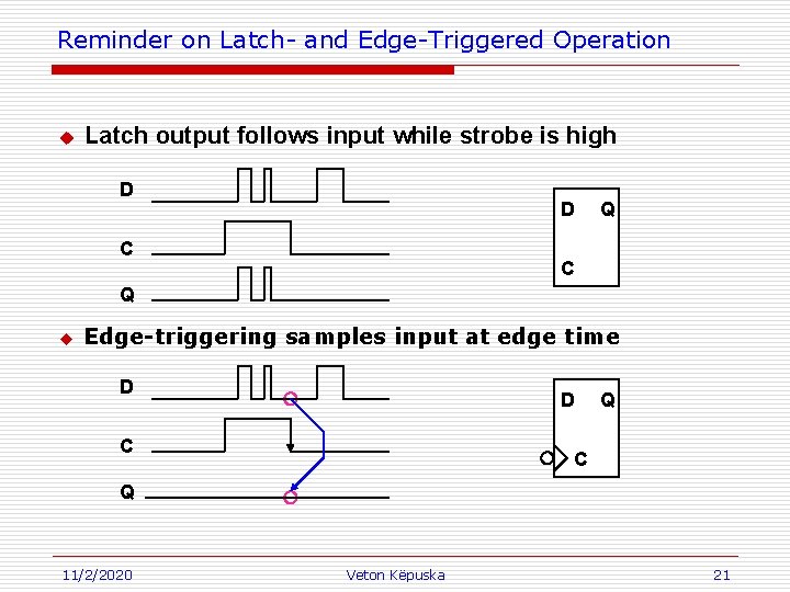
Data Path/Control Unit Separation u u Interface between data path and control consists of gate and strobe signals A gate selects one of several values to apply to a common point, say a bus A strobe changes the values of the flip-flops in a register to match new inputs The type of flip-flop used in registers has much influence on control and some on data path n n 11/2/2020 Latch: simpler hardware, but more complex timing Edge triggering: simpler timing, but about twice the hardware Veton Këpuska 20

Reminder on Latch- and Edge-Triggered Operation u Latch output follows input while strobe is high D D C Q u Edge-triggering samples input at edge time D D C Q 11/2/2020 Veton Këpuska 21

Logic Design for the 1 -Bus SRC u In the following section a design of SRC will be developed down to the gate level. n n Overview of the design Develop each of the blocks at the gate level. u u 11/2/2020 Design of the data path hardware Memory interface Design of IR hardware from which most of the control signals are developed. Design of the control unit. Veton Këpuska 22

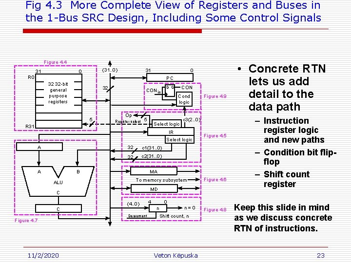
Fig 4. 3 More Complete View of Registers and Buses in the 1 -Bus SRC Design, Including Some Control Signals Figure 4. 4 31 á 31. . 0ñ 0 31 0 R 0 PC 32 32 -bit general purpose registers 32 5 CON in Op Register select 5 CON D Q Cond logic Select logic R 31 c 3á 2. . 0ñ IR Select logic A A 32 c 1á 31. . 0ñ 32 c 2á 31. . 0ñ To memory subsystem Figure 4. 7 11/2/2020 Figure 4. 6 MD C C Figure 4. 5 MA B ALU Figure 4. 9 á 4. . 0ñ Decrement 4 0 n n=0 Shift count, n Veton Këpuska Figure 4. 8 • Concrete RTN lets us add detail to the data path – Instruction register logic and new paths – Condition bit flipflop – Shift count register Keep this slide in mind as we discuss concrete RTN of instructions. 23

Gate-Level Design of SRC u In this section we will fill in the blocks shown in Figure 4. 3 presented in previous slide. n n n n 11/2/2020 Describe control signals that implement the RTN of the instructions in the preceding discussion. Start with Register File Extraction of c 1 and c 2 constant fields and the opcode field from instruction register. Design of the memory interface. Describe the instruction fetch and the add, addi , ld and st instruction’s control sequences. Design of n – shift count register and the shr instruction Conclude with description of the condition register and the br instruction. Veton Këpuska 24

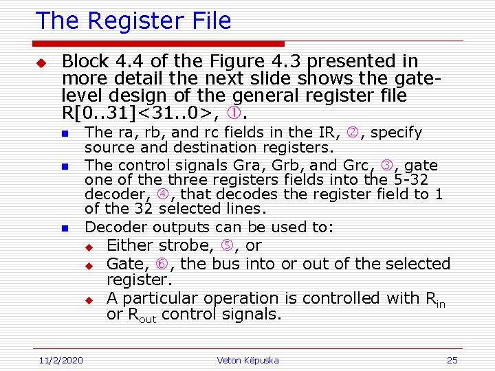
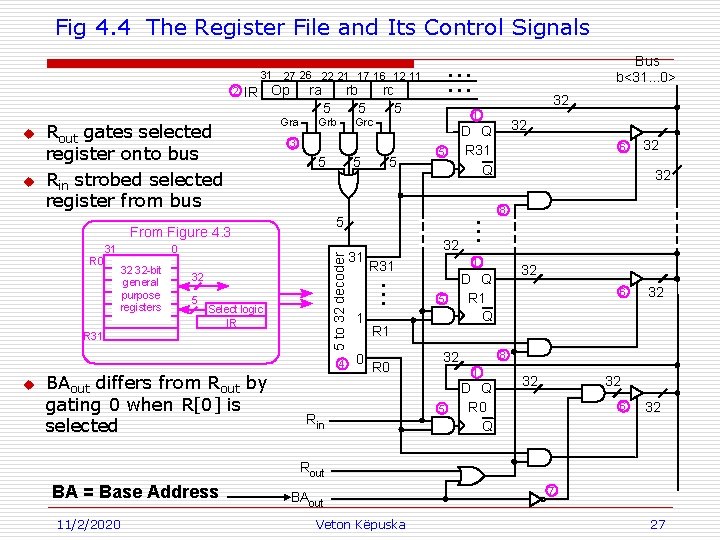
The Register File u Block 4. 4 of the Figure 4. 3 presented in more detail the next slide shows the gatelevel design of the general register file R[0. . 31]<31. . 0>, . n n n 11/2/2020 The ra, rb, and rc fields in the IR, , specify source and destination registers. The control signals Gra, Grb, and Grc, , gate one of the three registers fields into the 5 -32 decoder, , that decodes the register field to 1 of the 32 selected lines. Decoder outputs can be used to: u Either strobe, , or u Gate, , the bus into or out of the selected register. u A particular operation is controlled with Rin or Rout control signals. Veton Këpuska 25

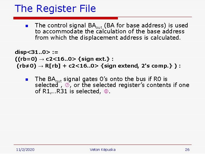
The Register File n The control signal BAout (BA for base address) is used to accommodate the calculation of the base address from which the displacement address is calculated. disp<31. . 0> : = ((rb=0) → c 2<16. . 0> {sign ext. } : (rb≠ 0) → R[rb] + c 2<16. . 0> {sign extend, 2's comp. } ) : n 11/2/2020 The BAout signal gates 0’s onto the bus if R 0 is selected , , or the selected register’s contents if one of R 1, . . R 31 is selected, . Veton Këpuska 26

Fig 4. 4 The Register File and Its Control Signals u Rout gates selected register onto bus Rin strobed selected register from bus ra Gra rb 5 Grb 5 0 32 32 -bit general purpose registers 32 5 Select logic IR R 31 4 u BAout differs from Rout by gating 0 when R[0] is selected 5 32 D Q R 31 Q 6 32 32 8 5 5 to 32 decoder R 0 5 5 32 1 Grc 3 From Figure 4. 3 31 5 rc 5 31 32 1 0 1 R 31 5 R 1 R 0 Rin . . . u IR Op . . . 2 Bus b<31. . . 0> . . . 31 27 26 22 21 17 16 12 11 6 32 8 32 1 5 32 D Q R 1 Q D Q R 0 Q 32 32 6 32 Rout BA = Base Address 11/2/2020 BAout Veton Këpuska 7 27

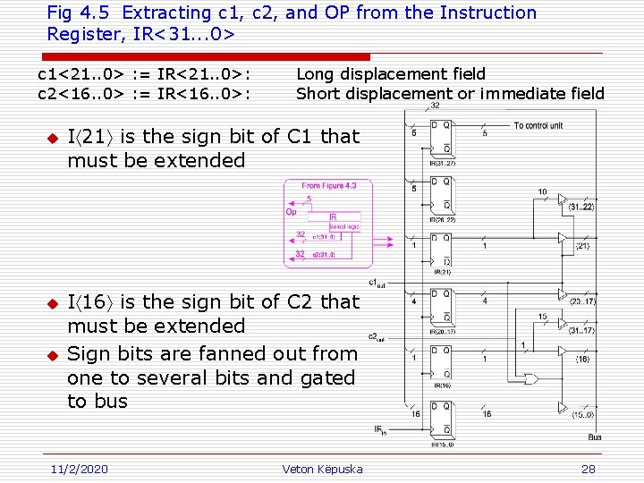
Fig 4. 5 Extracting c 1, c 2, and OP from the Instruction Register, IR<31. . . 0> c 1<21. . 0> : = IR<21. . 0>: c 2<16. . 0> : = IR<16. . 0>: u u u Long displacement field Short displacement or immediate field Iá 21ñ is the sign bit of C 1 that must be extended Iá 16ñ is the sign bit of C 2 that must be extended Sign bits are fanned out from one to several bits and gated to bus 11/2/2020 Veton Këpuska 28

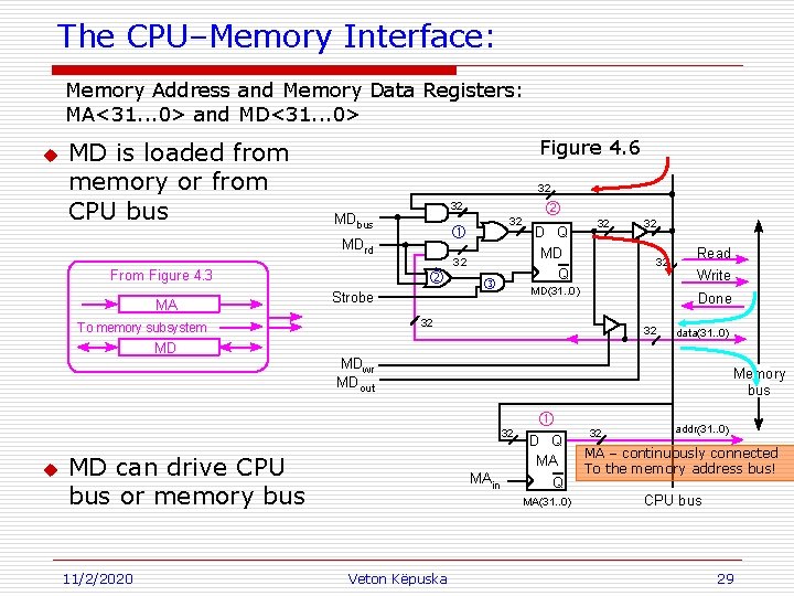
The CPU–Memory Interface: Memory Address and Memory Data Registers: MA<31. . . 0> and MD<31. . . 0> u MD is loaded from memory or from CPU bus Figure 4. 6 32 32 MDbus MDrd From Figure 4. 3 MA 32 Strobe 32 32 32 Read Write Done 32 dataá 31. . 0ñ MDwr MDout MD can drive CPU bus or memory bus 11/2/2020 D Q MDá 31. . 0ñ Memory bus 32 u 32 To memory subsystem MD 32 MAin D Q MAá 31. . 0ñ Veton Këpuska 32 addrá 31. . 0ñ MA – continuously connected To the memory address bus! CPU bus 29

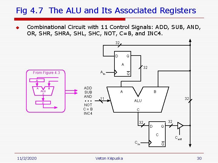
Fig 4. 7 The ALU and Its Associated Registers u Combinational Circuit with 11 Control Signals: ADD, SUB, AND, OR, SHRA, SHL, SHC, NOT, C=B, and INC 4. 32 D Q A A in From Figure 4. 3 32 Q A A ALU C C B ADD SUB AND . . . A 11 NOT C=B INC 4 B 32 ALU C 32 32 D Q C Cin 11/2/2020 Veton Këpuska C out Q 30

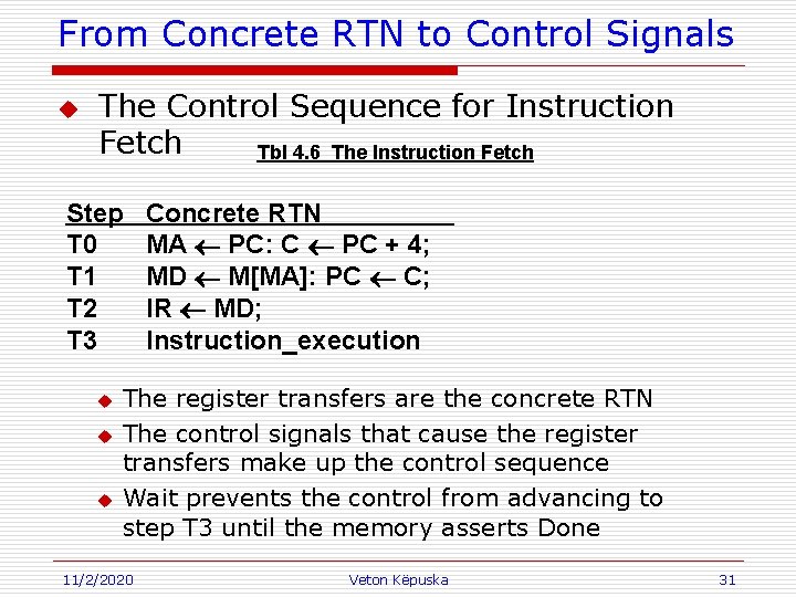
From Concrete RTN to Control Signals u The Control Sequence for Instruction Fetch Tbl 4. 6 The Instruction Fetch Step T 0 T 1 T 2 T 3 u u u Concrete RTN MA ¬ PC: C ¬ PC + 4; MD ¬ M[MA]: PC ¬ C; IR ¬ MD; Instruction_execution Control Sequence PCout, MAin, INC 4, Cin Read, Cout, PCin, Wait MDout, IRin The register transfers are the concrete RTN The control signals that cause the register transfers make up the control sequence Wait prevents the control from advancing to step T 3 until the memory asserts Done 11/2/2020 Veton Këpuska 31

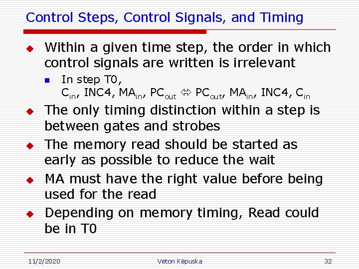
Control Steps, Control Signals, and Timing u Within a given time step, the order in which control signals are written is irrelevant n u u In step T 0, Cin, INC 4, MAin, PCout, MAin, INC 4, Cin The only timing distinction within a step is between gates and strobes The memory read should be started as early as possible to reduce the wait MA must have the right value before being used for the read Depending on memory timing, Read could be in T 0 11/2/2020 Veton Këpuska 32
![Control Sequence for the SRC add op 12 Rra Control Sequence for the SRC add (: = op = 12) ® R[ra] ¬](https://slidetodoc.com/presentation_image/442c20e15053160a6f4c17b6711db3fa/image-33.jpg)
Control Sequence for the SRC add (: = op = 12) ® R[ra] ¬ R[rb] + R[rc]: Tbl 4. 7 The add Instruction Step T 0 T 1 T 2 T 3 T 4 T 5 u u Concrete RTN MA ¬ PC: C ¬ PC + 4; MD ¬ M[MA]: PC ¬ C; IR ¬ MD; A ¬ R[rb]; C ¬ A + R[rc]; R[ra] ¬ C; Control Sequence PCout, MAin, INC 4, Cin Cout, PCin, Read, Wait MDout, IRin Grb, Rout, Ain Grc, Rout, ADD, Cin Cout, Gra, Rin, End Note the use of Gra, Grb, and Grc to gate the correct 5 -bit register select code to the registers End signals the control to start over at step T 0 11/2/2020 Veton Këpuska 33
![Control Sequence for the SRC addi op 13 Rra Rrb Control Sequence for the SRC addi (: = op= 13) ® R[ra] ¬ R[rb]](https://slidetodoc.com/presentation_image/442c20e15053160a6f4c17b6711db3fa/image-34.jpg)
Control Sequence for the SRC addi (: = op= 13) ® R[ra] ¬ R[rb] + c 2á 16. . 0ñ {2’s comp. , sign ext. } : Tbl 4. 8 The addi Instruction Step T 0. T 1. T 2. T 3. T 4. T 5. u Concrete RTN MA ¬ PC: C ¬ PC + 4; MD ¬ M[MA]; PC ¬ C; IR ¬ MD; A ¬ R[rb]; C ¬ A + c 2á 16. . 0ñ {sign ext. }; R[ra] ¬ C; Control Sequence PCout, MAin, Inc 4, Cin Cout, PCin, Read, Wait MDout, IRin Grb, Rout, Ain c 2 out, ADD, Cin Cout, Gra, Rin, End The c 2 out signal sign extends IRá 16. . 0ñ and gates it to the bus 11/2/2020 Veton Këpuska 34
![Control Sequence for the SRC st st op 3 Mdisp Control Sequence for the SRC st st (: = op = 3) ® M[disp]](https://slidetodoc.com/presentation_image/442c20e15053160a6f4c17b6711db3fa/image-35.jpg)
Control Sequence for the SRC st st (: = op = 3) ® M[disp] ¬ R[ra] : dispá 31. . 0ñ : = ((rb=0) ® c 2á 16. . 0ñ {sign extend} : (rb¹ 0) ® R[rb] + c 2á 16. . 0ñ {sign extend, 2’s complement}) ; The st Instruction Step T 0–T 2 T 3 T 4 T 5 T 6 T 7 u Concrete RTN Control Sequence Instruction fetch A ¬ (rb=0) ® 0: rb ¹ 0 ® R[rb]; Grb, BAout, Ain C ¬ A + c 2á 16. . 0ñ {sign-extend}; c 2 out, ADD, Cin MA ¬ C; Cout, MAin MD ¬ R[ra]; Gra, Rout, MDin, Write M[MA] ¬ MD; Wait, End Note BAout in T 3 compared to Rout in T 3 of addi 11/2/2020 Veton Këpuska 35
![Control Sequence for the SRC ld ld op 1 Rra Control Sequence for the SRC ld ld (: = op = 1) ® R[ra]](https://slidetodoc.com/presentation_image/442c20e15053160a6f4c17b6711db3fa/image-36.jpg)
Control Sequence for the SRC ld ld (: = op = 1) ® R[ra] ¬ M[disp] : dispá 31. . 0ñ : = ((rb=0) ® c 2á 16. . 0ñ {sign extend} : (rb¹ 0) ® R[rb] + c 2á 16. . 0ñ {sign extend, 2’s complement}) ; The ld Instruction Step T 0–T 2 T 3 T 4 T 5 T 6 T 7 u Concrete RTN Control Sequence Instruction fetch A ¬ (rb=0) ® 0: rb ¹ 0 ® R[rb]; Grb, BAout, Ain C ¬ A + c 2á 16. . 0ñ {sign-extend}; c 2 out, ADD, Cin MA ¬ C; Cout, MAin MD ¬ M[MA]; Read, Wait, MDrd, strobe R[ra] ¬ MD; Gra, Rin, MDout End Note that control signals MDrd and strobe as depicted from Figure 4. 6, are being used to strobe data form memory bus into MD. However, they are not shown (e. g. they are shown in red) in the table above because it is assumed that the memory system is responsible for asserting these signals. 11/2/2020 Veton Këpuska 36

The Shift Counter u The concrete RTN for shr relies upon a 5 -bit register to hold the shift count It must load, decrement, and have an “= 0” test u Fig 4. 8 u Bus From Figure 4. 3 4 á 4. . 0ñ 0 Decrement 11/2/2020 n=0 n 32 5 á 4. . 0ñ Decr Shift count, n X Y X⊕Y 0 0 1 1 1 0 Ld n: shift count 5 -bit down counter n = Q 4. . Q 0 á 31. . 0ñ n=0 Veton Këpuska 37

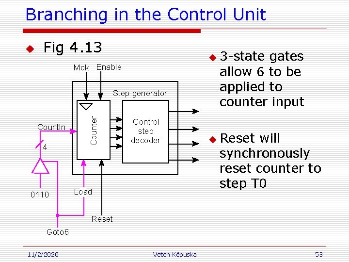
Control Sequence for the SRC shr Looping u Step T 0–T 2 T 3 T 4 T 5 T 6 T 7 u u Concrete RTN Instruction fetch n ¬ IRá 4. . 0ñ; (n=0) ® (n ¬ R[rc]á 4. . 0ñ); C ¬ R[rb]; Shr (: = (n¹ 0) ® (Cá 31. . 0ñ ¬ 0#Cá 31. . 1ñ: n ¬ n-1; Shr) ); R[ra] ¬ C; Control Sequence Instruction fetch c 1 out, Ld n=0 ® (Grc, Rout, Ld) Grb, Rout, C=B, Cin n¹ 0 ® (Cout, SHR, Cin, Decr, Goto 6) Cout, Gra, Rin, End Conditional control signals and repeating a control step are new concepts Barrel shifter design enables 1 cycle shift. 11/2/2020 Veton Këpuska 38

Branching cond : = ( c 3á 2. . 0ñ=0 ® 0: c 3á 2. . 0ñ = 1 ® 1: c 3á 2. . 0ñ = 2 ® R[rc] = 0: c 3á 2. . 0ñ = 3 ® R[rc] ¹ 0: c 3á 2. . 0ñ = 4 ® R[rc]á 31ñ = 0: c 3á 2. . 0ñ = 5 ® R[rc]á 31ñ = 1 ): u This is equivalent to the logic expression cond = 11/2/2020 (c 3á 2. . 0ñ = 1) Ú (c 3á 2. . 0ñ = 2)Ù(R[rc] = 0) Ú (c 3á 2. . 0ñ = 3)ÙØ(R[rc] = 0) Ú (c 3á 2. . 0ñ = 4)ÙØR[rc]á 31ñ Ú (c 3á 2. . 0ñ = 5)ÙR[rc]á 31ñ Veton Këpuska 39

Computation of the Conditional Value CON IRá 2. . 0ñ 3 From Figure 4. 3 32 CONin D Q Bus Decoder 5 4 3 2 1 CON Cond logic =0 ¹ 0 á 31ñ ³ 0 <0 á 31. . 0ñ u 0 1 32 c 3á 2. . 0ñ 0 CONin D Q CON Q NOR gate does “= 0” test of R[rc] on processor bus 11/2/2020 Veton Këpuska 40

Control Sequence for SRC Branch br br (: = op = 8) ® (cond ® PC ¬ R[rb]): Step T 0–T 2 T 3 T 4 u u Concrete RTN Instruction fetch CON ¬ cond(R[rc]); CON ® PC ¬ R[rb]; Control Sequence Instruction fetch Grc, Rout, CONin Grb, Rout, CON ® PCin, End Condition logic is always connected to CON, so R[rc] only needs to be put on bus in T 3 Only PCin is conditional in T 4 since gating R[rb] to bus makes no difference if it is not used 11/2/2020 Veton Këpuska 41

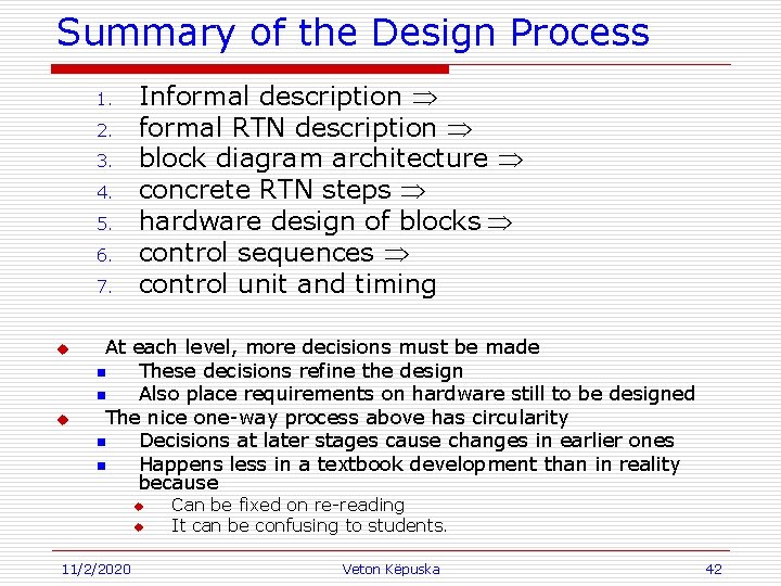
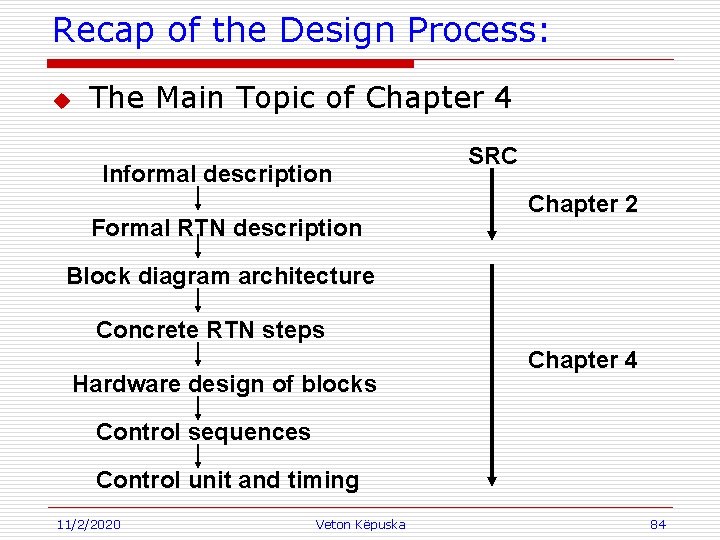
Summary of the Design Process 1. 2. 3. 4. 5. 6. 7. u u Informal description Þ formal RTN description Þ block diagram architecture Þ concrete RTN steps Þ hardware design of blocks Þ control sequences Þ control unit and timing At each level, more decisions must be made n These decisions refine the design n Also place requirements on hardware still to be designed The nice one-way process above has circularity n Decisions at later stages cause changes in earlier ones n Happens less in a textbook development than in reality because u u 11/2/2020 Can be fixed on re-reading It can be confusing to students. Veton Këpuska 42

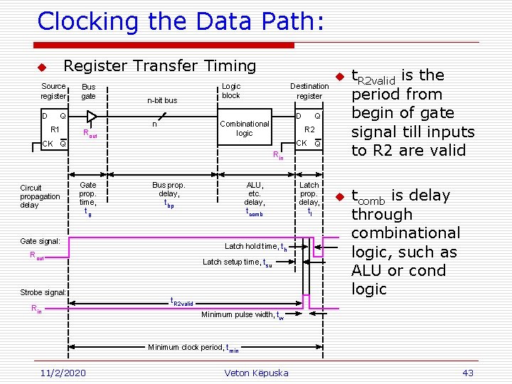
Clocking the Data Path: Register Transfer Timing u Source register D Bus gate Q R 1 Rout n-bit bus Logic block Destination register D Combinational logic n u Q R 2 CK Q Rin Circuit propagation delay Gate prop. time, tg Bus prop. delay, tbp Gate signal: Latch hold time, th Rout Strobe signal: Rin ALU, etc. delay, tcomb Latch setup time, tsu t. R 2 valid Latch prop. delay, tl u t. R 2 valid is the period from begin of gate signal till inputs to R 2 are valid tcomb is delay through combinational logic, such as ALU or cond logic Minimum pulse width, tw Minimum clock period, tmin 11/2/2020 Veton Këpuska 43

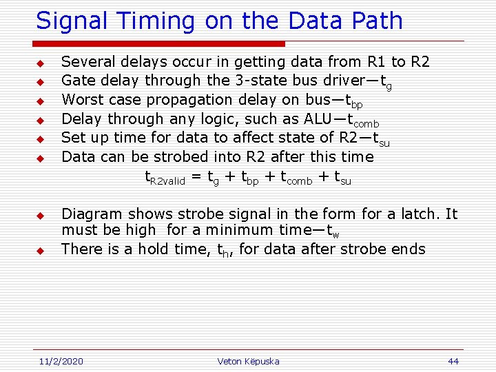
Signal Timing on the Data Path u u u u Several delays occur in getting data from R 1 to R 2 Gate delay through the 3 -state bus driver—tg Worst case propagation delay on bus—tbp Delay through any logic, such as ALU—tcomb Set up time for data to affect state of R 2—tsu Data can be strobed into R 2 after this time t. R 2 valid = tg + tbp + tcomb + tsu Diagram shows strobe signal in the form for a latch. It must be high for a minimum time—tw There is a hold time, th, for data after strobe ends 11/2/2020 Veton Këpuska 44

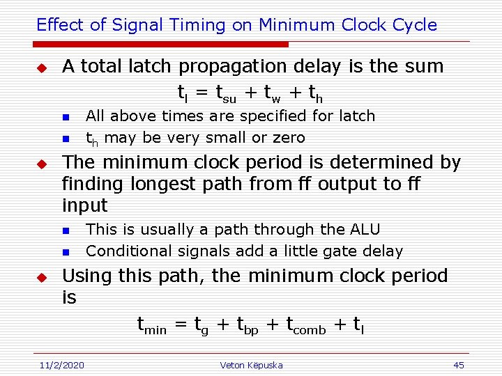
Effect of Signal Timing on Minimum Clock Cycle u A total latch propagation delay is the sum tl = tsu + tw + th n n u The minimum clock period is determined by finding longest path from ff output to ff input n n u All above times are specified for latch th may be very small or zero This is usually a path through the ALU Conditional signals add a little gate delay Using this path, the minimum clock period is tmin = tg + tbp + tcomb + tl 11/2/2020 Veton Këpuska 45

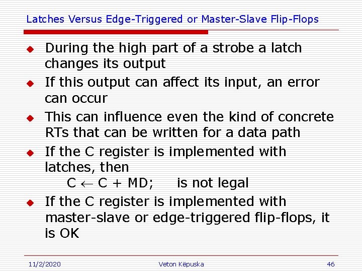
Latches Versus Edge-Triggered or Master-Slave Flip-Flops u u u During the high part of a strobe a latch changes its output If this output can affect its input, an error can occur This can influence even the kind of concrete RTs that can be written for a data path If the C register is implemented with latches, then C ¬ C + MD; is not legal If the C register is implemented with master-slave or edge-triggered flip-flops, it is OK 11/2/2020 Veton Këpuska 46

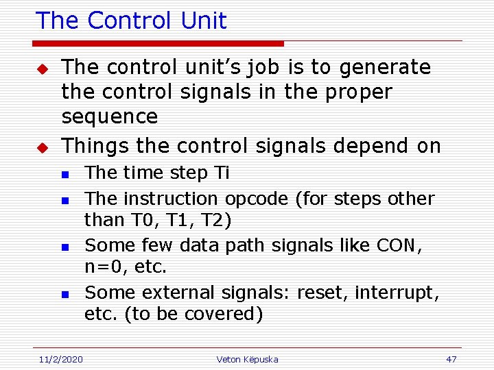
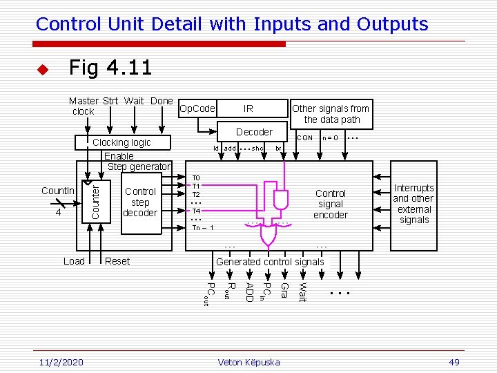
The Control Unit u u The control unit’s job is to generate the control signals in the proper sequence Things the control signals depend on n n 11/2/2020 The time step Ti The instruction opcode (for steps other than T 0, T 1, T 2) Some few data path signals like CON, n=0, etc. Some external signals: reset, interrupt, etc. (to be covered) Veton Këpuska 47

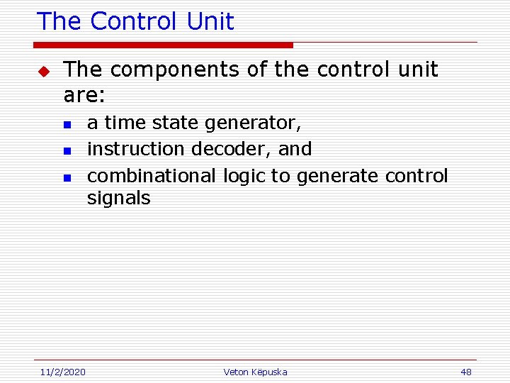
The Control Unit u The components of the control unit are: n n n 11/2/2020 a time state generator, instruction decoder, and combinational logic to generate control signals Veton Këpuska 48

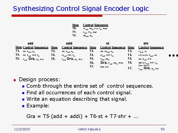
Control Unit Detail with Inputs and Outputs Fig 4. 11 u Master Strt Wait Done Op. Code clock IR Other signals from the data path Decoder Countln 4 Counter Clocking logic Enable Step generator Control step decoder ld add . . . shc CON Control signal encoder . . . T 4 . . . Tn – 1 . . . Load Reset Interrupts and other external signals . . . Generated control signals Veton Këpuska Wait Gra PCin ADD Rout PCout 11/2/2020 . . . br T 0 T 1 T 2 . . . n=0 . . . 49

Synthesizing Control Signal Encoder Logic Step Control Sequence T 0. T 1. T 2. add PCout, MA in, Inc 4, Cin, Read Cout, PCin, Wait MD , IR out in addi st shr Step Control Sequence T 3. Grb, R , A Grb, BA , A c 1 , Ld T 3. out in out T 4. Grc, R , ADD, C c 2 , ADD, C n=0 ® (Grc, R , Ld) T 4. out in out Cout, MAin Grb, Rout, C=B T 5. C , R , End C , R , End T 5. out Gra, in n¹ 0 ® (Cout, SHR, Cin, T 6. Gra, Rout, MDin, Write T 6. Decr, Goto 7) Wait, End T 7. C , R , End T 7. out Gra, in u Design process: n Comb through the entire set of control sequences. n Find all occurrences of each control signal. n Write an equation describing that signal. n Example: Gra = T 5·(add + addi) + T 6·st + T 7·shr +. . . 11/2/2020 Veton Këpuska 50

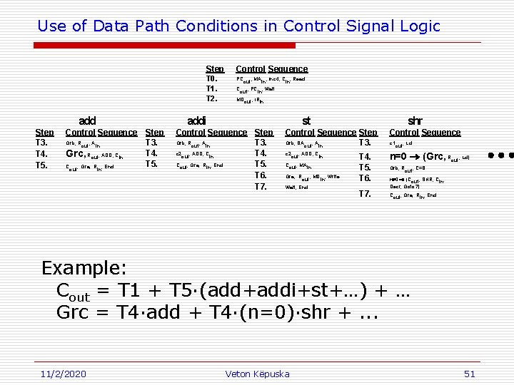
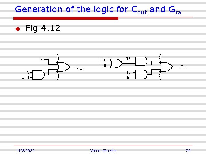
Use of Data Path Conditions in Control Signal Logic Step Control Sequence T 0. T 1. T 2. add PCout, MAin, Inc 4, Cin, Read Cout, PCin, Wait MDout, IRin addi st shr Step Control Sequence Grb, R , A Grb, BA , A c 1 , Ld T 3. out in out c 2 , ADD, C T 4. Grc, Rout, ADD, Cin out in T 4. n=0 ® (Grc, Rout, Ld) C , Gra, R , End C , MA T 5. Cout, Gra, Rin, End T 5. out in Grb, Rout, C=B T 5. Gra, Rout, MDin, Write T 6. n¹ 0 ® (C , SHR, C , T 6. out in Decr, Goto 7) Wait, End T 7. Cout, Gra, Rin, End T 7. Example: Cout = T 1 + T 5·(add+addi+st+…) + … Grc = T 4·add + T 4·(n=0)·shr +. . . 11/2/2020 Veton Këpuska 51

Generation of the logic for Cout and Gra T 5 add 11/2/2020 Cout T 5 Gra T 7 ld Veton Këpuska . . . addi . . . T 1 . . . Fig 4. 12 . . . u 52

Branching in the Control Unit u Fig 4. 13 u Mck Enable Countln 4 0110 Counter Step generator Control step decoder Load u 3 -state gates allow 6 to be applied to counter input Reset will synchronously reset counter to step T 0 Reset Goto 6 11/2/2020 Veton Këpuska 53

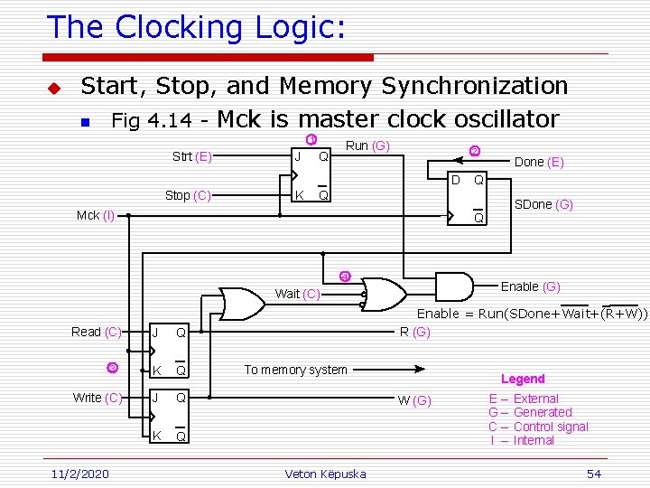
The Clocking Logic: u Start, Stop, and Memory Synchronization n Fig 4. 14 - Mck is master clock oscillator 1 Strt (E) J Q Run (G) 2 D Stop (C) K SDone (G) Q 4 Enable (G) Wait (C) 3 Write (C) 11/2/2020 Q Q Mck (I) Read (C) Done (E) J Q K Q Enable = Run(SDone+Wait+(R+W)) R (G) To memory system Legend W (G) Veton Këpuska E– G– C– I – External Generated Control signal Internal 54

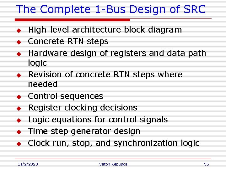
The Complete 1 -Bus Design of SRC u u u u u High-level architecture block diagram Concrete RTN steps Hardware design of registers and data path logic Revision of concrete RTN steps where needed Control sequences Register clocking decisions Logic equations for control signals Time step generator design Clock run, stop, and synchronization logic 11/2/2020 Veton Këpuska 55

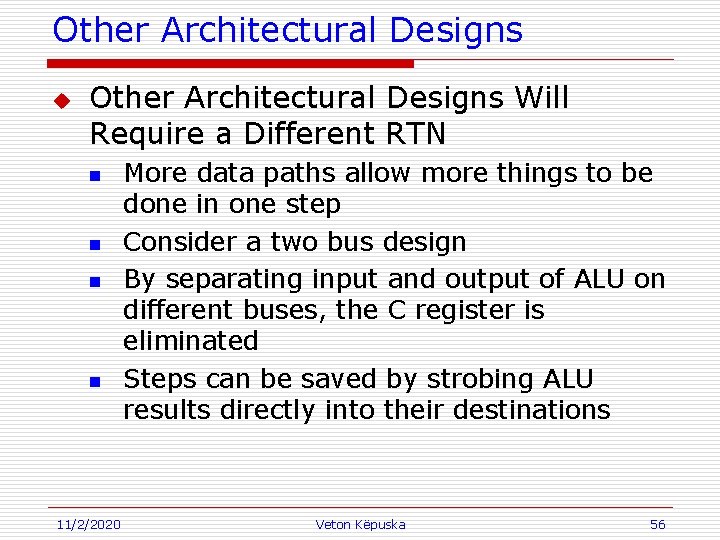
Other Architectural Designs u Other Architectural Designs Will Require a Different RTN n n 11/2/2020 More data paths allow more things to be done in one step Consider a two bus design By separating input and output of ALU on different buses, the C register is eliminated Steps can be saved by strobing ALU results directly into their destinations Veton Këpuska 56

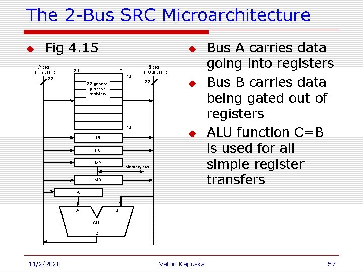
The 2 -Bus SRC Microarchitecture u Fig 4. 15 A bus (“ In bus” ) 32 u 31 0 R 0 B bus (“Out bus” ) 32 32 general purpose registers R 31 IR u u PC MA Memory bus MD Bus A carries data going into registers Bus B carries data being gated out of registers ALU function C=B is used for all simple register transfers A A B ALU C 11/2/2020 Veton Këpuska 57

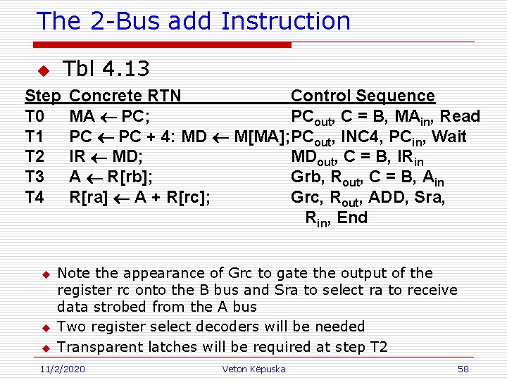
The 2 -Bus add Instruction Tbl 4. 13 u Step T 0 T 1 T 2 T 3 T 4 u u u Concrete RTN Control Sequence MA ¬ PC; PCout, C = B, MAin, Read PC ¬ PC + 4: MD ¬ M[MA]; PCout, INC 4, PCin, Wait IR ¬ MD; MDout, C = B, IRin A ¬ R[rb]; Grb, Rout, C = B, Ain R[ra] ¬ A + R[rc]; Grc, Rout, ADD, Sra, Rin, End Note the appearance of Grc to gate the output of the register rc onto the B bus and Sra to select ra to receive data strobed from the A bus Two register select decoders will be needed Transparent latches will be required at step T 2 11/2/2020 Veton Këpuska 58

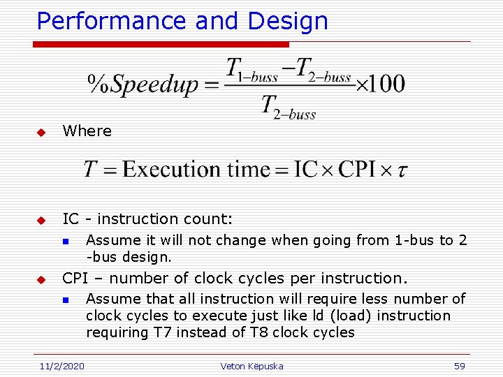
Performance and Design u Where u IC - instruction count: n u Assume it will not change when going from 1 -bus to 2 -bus design. CPI – number of clock cycles per instruction. n 11/2/2020 Assume that all instruction will require less number of clock cycles to execute just like ld (load) instruction requiring T 7 instead of T 8 clock cycles Veton Këpuska 59

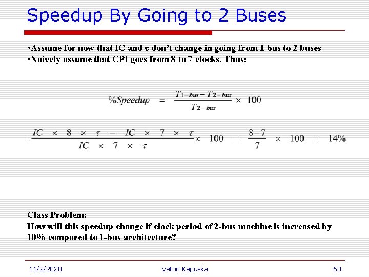
Speedup By Going to 2 Buses • Assume for now that IC and t don’t change in going from 1 bus to 2 buses • Naively assume that CPI goes from 8 to 7 clocks. Thus: Class Problem: How will this speedup change if clock period of 2 -bus machine is increased by 10% compared to 1 -bus architecture? 11/2/2020 Veton Këpuska 60

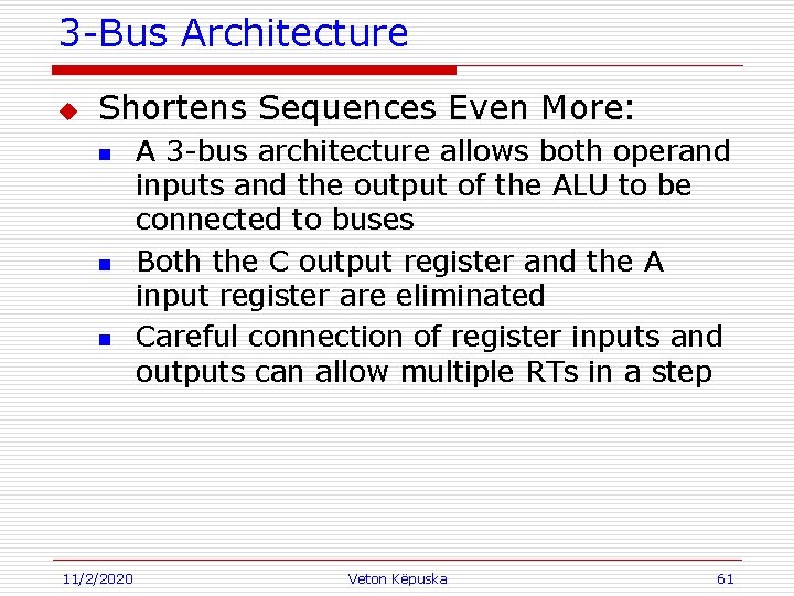
3 -Bus Architecture u Shortens Sequences Even More: n n n 11/2/2020 A 3 -bus architecture allows both operand inputs and the output of the ALU to be connected to buses Both the C output register and the A input register are eliminated Careful connection of register inputs and outputs can allow multiple RTs in a step Veton Këpuska 61

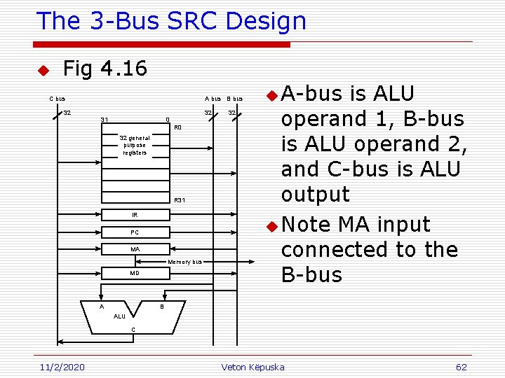
The 3 -Bus SRC Design u Fig 4. 16 C bus 32 A bus B bus 31 32 0 R 0 32 general purpose registers R 31 IR PC MA Memory bus MD A 32 u A-bus is ALU operand 1, B-bus is ALU operand 2, and C-bus is ALU output u Note MA input connected to the B-bus B ALU C 11/2/2020 Veton Këpuska 62

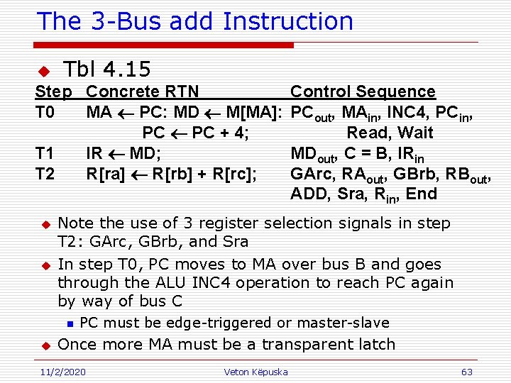
The 3 -Bus add Instruction u Tbl 4. 15 Step T 0 T 1 T 2 u u Note the use of 3 register selection signals in step T 2: GArc, GBrb, and Sra In step T 0, PC moves to MA over bus B and goes through the ALU INC 4 operation to reach PC again by way of bus C n u Concrete RTN Control Sequence MA ¬ PC: MD ¬ M[MA]: PCout, MAin, INC 4, PCin, PC ¬ PC + 4; Read, Wait IR ¬ MD; MDout, C = B, IRin R[ra] ¬ R[rb] + R[rc]; GArc, RAout, GBrb, RBout, ADD, Sra, Rin, End PC must be edge-triggered or master-slave Once more MA must be a transparent latch 11/2/2020 Veton Këpuska 63

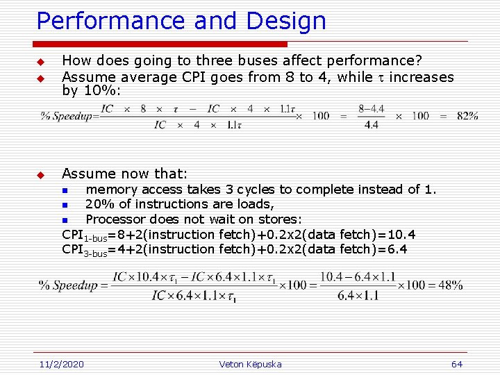
Performance and Design u How does going to three buses affect performance? Assume average CPI goes from 8 to 4, while t increases by 10%: u Assume now that: u memory access takes 3 cycles to complete instead of 1. n 20% of instructions are loads, n Processor does not wait on stores: CPI 1 -bus=8+2(instruction fetch)+0. 2 x 2(data fetch)=10. 4 CPI 3 -bus=4+2(instruction fetch)+0. 2 x 2(data fetch)=6. 4 n 11/2/2020 Veton Këpuska 64

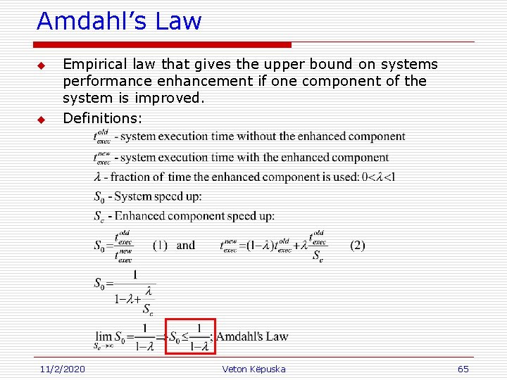
Amdahl’s Law u u Empirical law that gives the upper bound on systems performance enhancement if one component of the system is improved. Definitions: 11/2/2020 Veton Këpuska 65

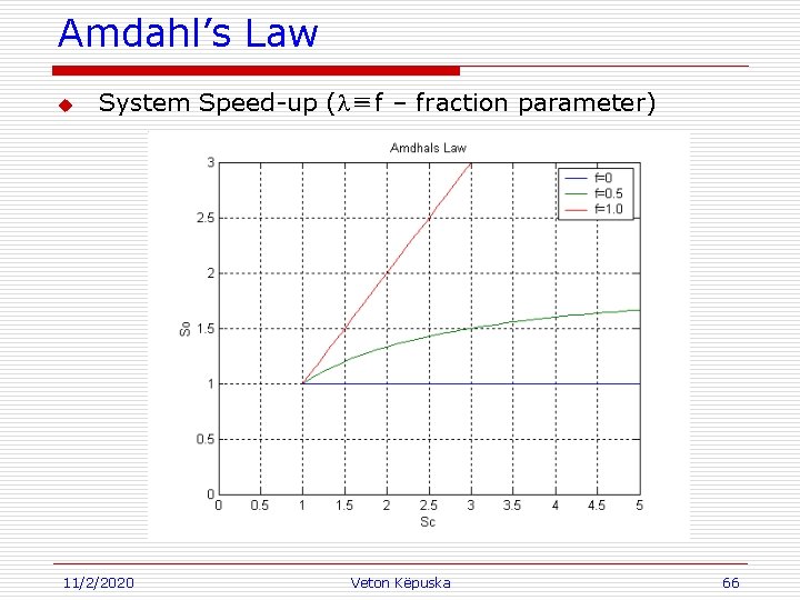
Amdahl’s Law u System Speed-up ( ≡f – fraction parameter) 11/2/2020 Veton Këpuska 66

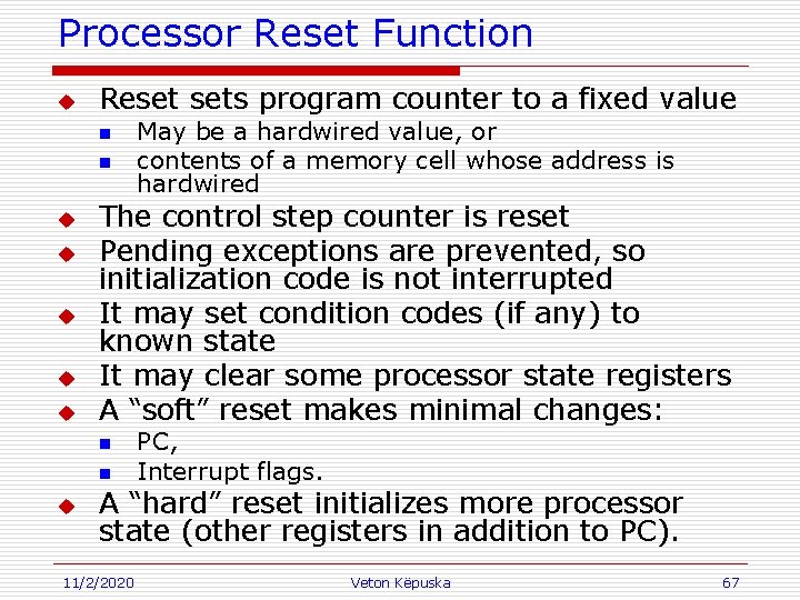
Processor Reset Function u Reset sets program counter to a fixed value n n u u u The control step counter is reset Pending exceptions are prevented, so initialization code is not interrupted It may set condition codes (if any) to known state It may clear some processor state registers A “soft” reset makes minimal changes: n n u May be a hardwired value, or contents of a memory cell whose address is hardwired PC, Interrupt flags. A “hard” reset initializes more processor state (other registers in addition to PC). 11/2/2020 Veton Këpuska 67

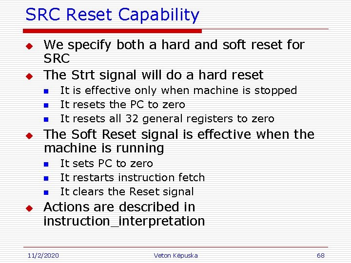
SRC Reset Capability u u We specify both a hard and soft reset for SRC The Strt signal will do a hard reset n n n u The Soft Reset signal is effective when the machine is running n n n u It is effective only when machine is stopped It resets the PC to zero It resets all 32 general registers to zero It sets PC to zero It restarts instruction fetch It clears the Reset signal Actions are described in instruction_interpretation 11/2/2020 Veton Këpuska 68

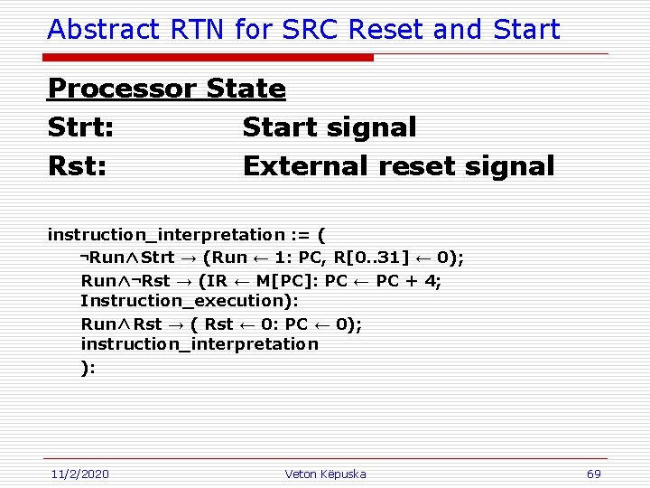
Abstract RTN for SRC Reset and Start Processor State Strt: Start signal Rst: External reset signal instruction_interpretation : = ( ¬Run∧Strt → (Run ← 1: PC, R[0. . 31] ← 0); Run∧¬Rst → (IR ← M[PC]: PC ← PC + 4; Instruction_execution): Run∧Rst → ( Rst ← 0: PC ← 0); instruction_interpretation ): 11/2/2020 Veton Këpuska 69

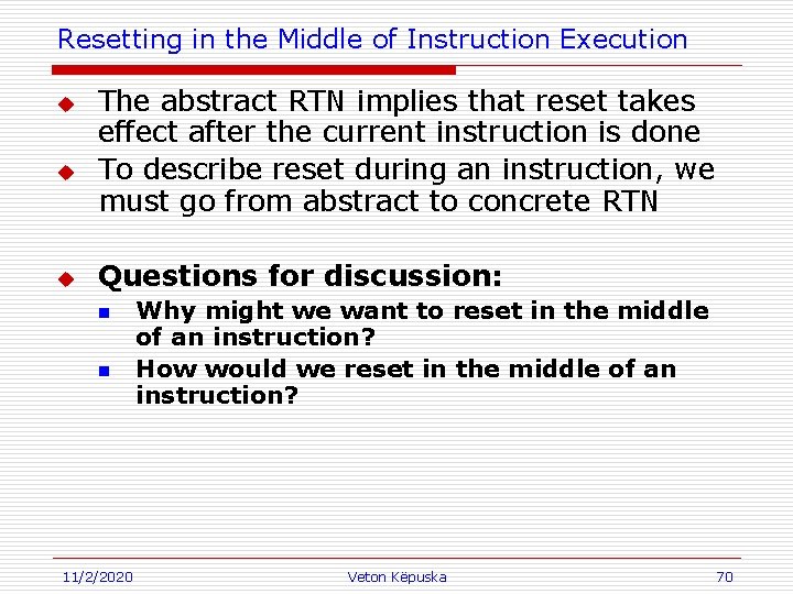
Resetting in the Middle of Instruction Execution u u u The abstract RTN implies that reset takes effect after the current instruction is done To describe reset during an instruction, we must go from abstract to concrete RTN Questions for discussion: n n 11/2/2020 Why might we want to reset in the middle of an instruction? How would we reset in the middle of an instruction? Veton Këpuska 70

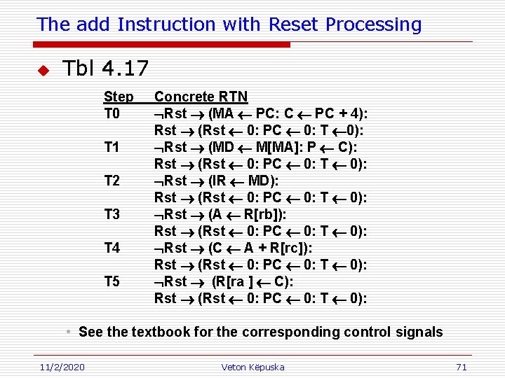
The add Instruction with Reset Processing u Tbl 4. 17 Step T 0 T 1 T 2 T 3 T 4 T 5 Concrete RTN ØRst ® (MA ¬ PC: C ¬ PC + 4): Rst ® (Rst ¬ 0: PC ¬ 0: T ¬ 0): ØRst ® (MD ¬ M[MA]: P ¬ C): Rst ® (Rst ¬ 0: PC ¬ 0: T ¬ 0): ØRst ® (IR ¬ MD): Rst ® (Rst ¬ 0: PC ¬ 0: T ¬ 0): ØRst ® (A ¬ R[rb]): Rst ® (Rst ¬ 0: PC ¬ 0: T ¬ 0): ØRst ® (C ¬ A + R[rc]): Rst ® (Rst ¬ 0: PC ¬ 0: T ¬ 0): ØRst ® (R[ra ] ¬ C): Rst ® (Rst ¬ 0: PC ¬ 0: T ¬ 0): • See the textbook for the corresponding control signals 11/2/2020 Veton Këpuska 71

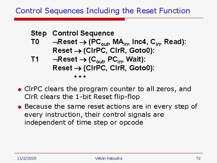
Control Sequences Including the Reset Function Step T 0 T 1 u u Control Sequence ØReset ® (PCout, MAin, Inc 4, Cin, Read): Reset ® (Clr. PC, Clr. R, Goto 0): ØReset ® (Cout, PCin, Wait): Reset ® (Clr. PC, Clr. R, Goto 0): • • • Clr. PC clears the program counter to all zeros, and Clr. R clears the 1 -bit Reset flip-flop Because the same reset actions are in every step of every instruction, their control signals are independent of time step or opcode 11/2/2020 Veton Këpuska 72

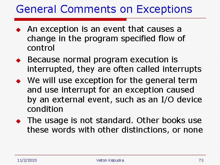
General Comments on Exceptions u u An exception is an event that causes a change in the program specified flow of control Because normal program execution is interrupted, they are often called interrupts We will use exception for the general term and use interrupt for an exception caused by an external event, such as an I/O device condition The usage is not standard. Other books use these words with other distinctions, or none 11/2/2020 Veton Këpuska 73

Combined Hardware/Software Response to an Exception u u u The system must control the type of exceptions it will process at any given time The state of the running program is saved when an allowed exception occurs Control is transferred to the correct software routine, or “handler, ” for this exception This exception, and others of less or equal importance, are disallowed during the handler The state of the interrupted program is restored at the end of execution of the handler 11/2/2020 Veton Këpuska 74

Hardware Required to Support Exceptions u u u To determine relative importance, a priority number is associated with every exception Hardware must save and change the PC, since without it no program execution is possible Hardware must disable the current exception lest is interrupt the handler before it can start Address of the handler is called the exception vector and is a hardware function of the exception type Exceptions must access a save area for PC and other hardware saved items n 11/2/2020 Choices are special registers or a hardware stack Veton Këpuska 75

New Instructions Needed to Support Exceptions u u An instruction executed at the end of the handler must reverse the state changes done by hardware when the exception occurred There must be instructions to control what exceptions are allowed n u The simplest of these enable or disable all exceptions If processor state is stored in special registers on an exception, instructions are needed to save and restore these registers 11/2/2020 Veton Këpuska 76

Kinds of Exceptions u u System reset Exceptions associated with memory access n n u u u Machine check exceptions Data access exceptions Instruction access exceptions Alignment exceptions Program exceptions Miscellaneous hardware exceptions Trace and debugging exceptions Non-maskable exceptions External exceptions—interrupts 11/2/2020 Veton Këpuska 77

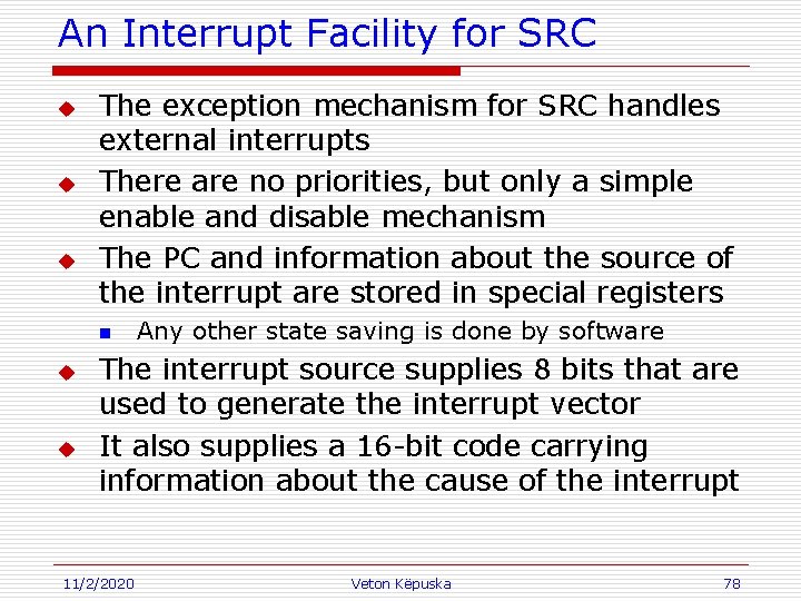
An Interrupt Facility for SRC u u u The exception mechanism for SRC handles external interrupts There are no priorities, but only a simple enable and disable mechanism The PC and information about the source of the interrupt are stored in special registers n u u Any other state saving is done by software The interrupt source supplies 8 bits that are used to generate the interrupt vector It also supplies a 16 -bit code carrying information about the cause of the interrupt 11/2/2020 Veton Këpuska 78

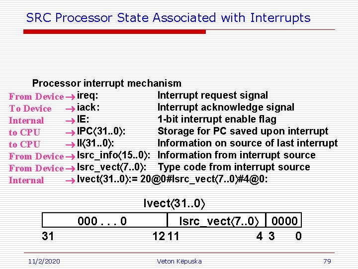
SRC Processor State Associated with Interrupts Processor interrupt mechanism Interrupt request signal From Device ® ireq: Interrupt acknowledge signal To Device ® iack: 1 -bit interrupt enable flag Internal ® IE: Storage for PC saved upon interrupt to CPU ® IPCá 31. . 0ñ: Information on source of last interrupt to CPU ® IIá 31. . 0ñ: From Device ® Isrc_infoá 15. . 0ñ: Information from interrupt source From Device ® Isrc_vectá 7. . 0ñ: Type code from interrupt source Internal ® Ivectá 31. . 0ñ: = 20@0#Isrc_vectá 7. . 0ñ#4@0: 000. . . 0 31 11/2/2020 Ivectá 31. . 0ñ Isrc_vectá 7. . 0ñ 0000 12 11 4 3 0 Veton Këpuska 79

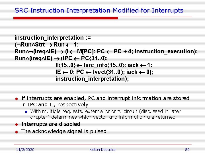
SRC Instruction Interpretation Modified for Interrupts instruction_interpretation : = (ØRunÙStrt ® Run ¬ 1: RunÙØ(ireqÙIE) ® (I ¬ M[PC]: PC ¬ PC + 4; instruction_execution): RunÙ(ireqÙIE) ® (IPC ¬ PC á 31. . 0ñ: IIá 15. . 0ñ ¬ Isrc_infoá 15. . 0ñ: iack ¬ 1: IE ¬ 0: PC ¬ Ivectá 31. . 0 ñ; iack ¬ 0); instruction_interpretation); u If interrupts are enabled, PC and interrupt information are stored in IPC and II, respectively n u u With multiple requests, external priority circuit (discussed in later chapter) determines which vector and information are returned Interrupts are disabled The acknowledge signal is pulsed 11/2/2020 Veton Këpuska 80

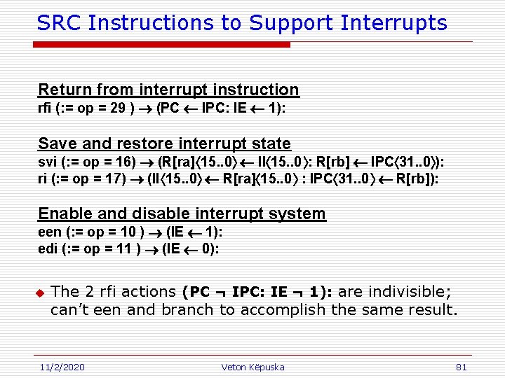
SRC Instructions to Support Interrupts Return from interrupt instruction rfi (: = op = 29 ) ® (PC ¬ IPC: IE ¬ 1): Save and restore interrupt state svi (: = op = 16) ® (R[ra] á 15. . 0ñ ¬ IIá 15. . 0 ñ: R[rb] ¬ IPCá 31. . 0ñ): ri (: = op = 17) ® (II á 15. . 0ñ ¬ R[ra]á 15. . 0 ñ : IPCá 31. . 0 ñ ¬ R[rb]): Enable and disable interrupt system een (: = op = 10 ) ® (IE ¬ 1): edi (: = op = 11 ) ® (IE ¬ 0): u The 2 rfi actions (PC ¬ IPC: IE ¬ 1): are indivisible; can’t een and branch to accomplish the same result. 11/2/2020 Veton Këpuska 81

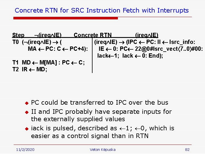
Concrete RTN for SRC Instruction Fetch with Interrupts Step Ø(ireqÙIE) Concrete RTN (ireqÙIE) T 0 (Ø(ireqÙIE) ® ( (ireqÙIE) ® (IPC ¬ PC: II ¬ Isrc_info: MA ¬ PC: C ¬ PC+4): IE ¬ 0: PC¬ 22@0#Isrc_vect á 7. . 0ñ#00: Iack¬ 1; Iack ¬ 0: End); T 1 MD ¬ M[MA] : PC ¬ C; T 2 IR ¬ MD; u u u PC could be transferred to IPC over the bus II and IPC probably have separate inputs for the externally supplied values iack is pulsed, described as ¬ 1; ¬ 0, which is easier as a control signal than in RTN 11/2/2020 Veton Këpuska 82

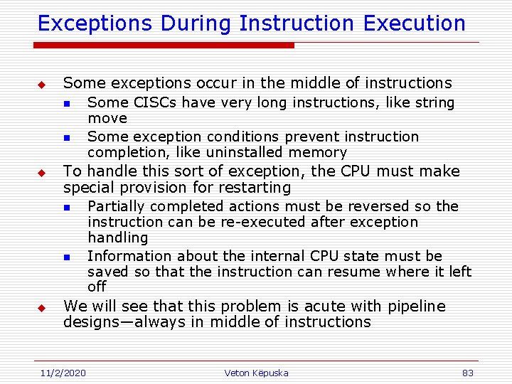
Exceptions During Instruction Execution u u u Some exceptions occur in the middle of instructions n Some CISCs have very long instructions, like string move n Some exception conditions prevent instruction completion, like uninstalled memory To handle this sort of exception, the CPU must make special provision for restarting n Partially completed actions must be reversed so the instruction can be re-executed after exception handling n Information about the internal CPU state must be saved so that the instruction can resume where it left off We will see that this problem is acute with pipeline designs—always in middle of instructions 11/2/2020 Veton Këpuska 83

Recap of the Design Process: u The Main Topic of Chapter 4 Informal description Formal RTN description SRC Chapter 2 Block diagram architecture Concrete RTN steps Hardware design of blocks Chapter 4 Control sequences Control unit and timing 11/2/2020 Veton Këpuska 84