Computer Architecture Principles Tradeoffs Chapter 6 Physical Memory



- Slides: 16

Computer Architecture: Principles & Tradeoffs Chapter 6: Physical Memory Yale Patt The University of Texas at Austin, Texas Fall, 2020

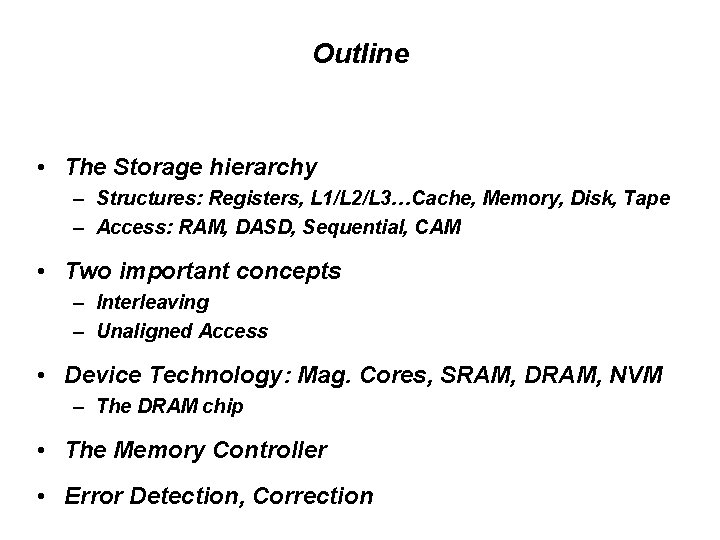
Outline • The Storage hierarchy – Structures: Registers, L 1/L 2/L 3…Cache, Memory, Disk, Tape – Access: RAM, DASD, Sequential, CAM • Two important concepts – Interleaving – Unaligned Access • Device Technology: Mag. Cores, SRAM, DRAM, NVM – The DRAM chip • The Memory Controller • Error Detection, Correction

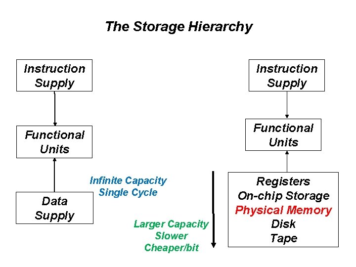
The Storage Hierarchy Instruction Supply Functional Units Data Supply Infinite Capacity Single Cycle Larger Capacity Slower Cheaper/bit Registers On-chip Storage Physical Memory Disk Tape

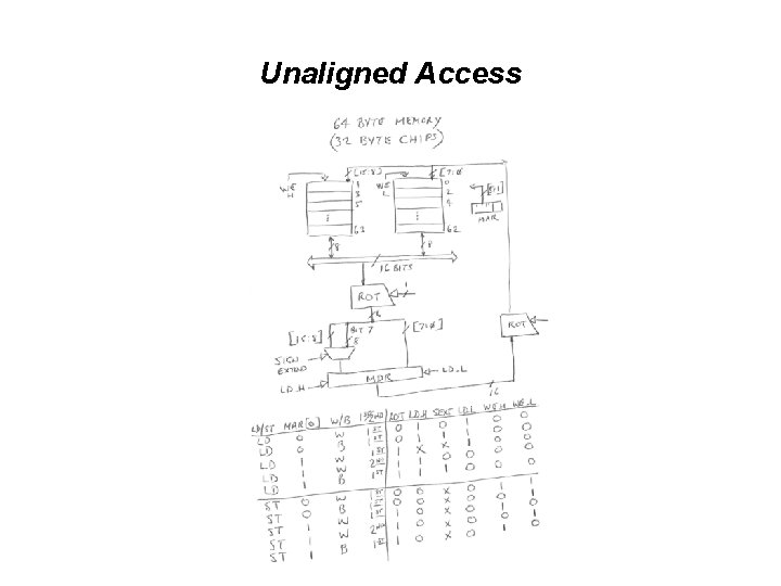
Unaligned Access

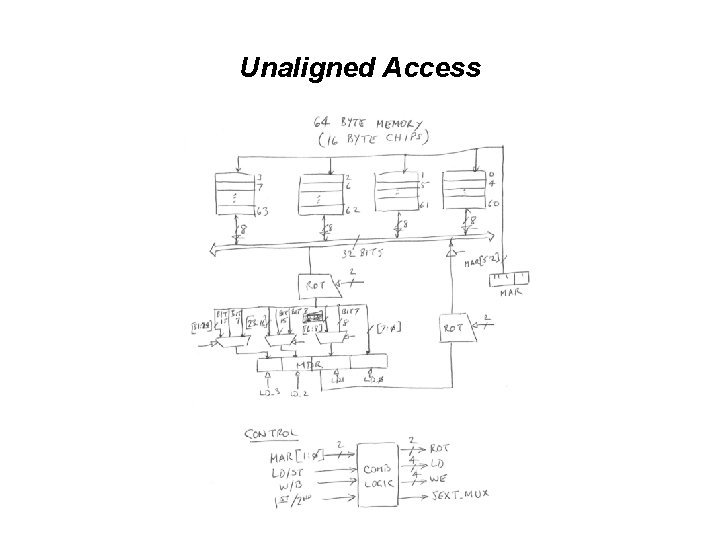
Unaligned Access

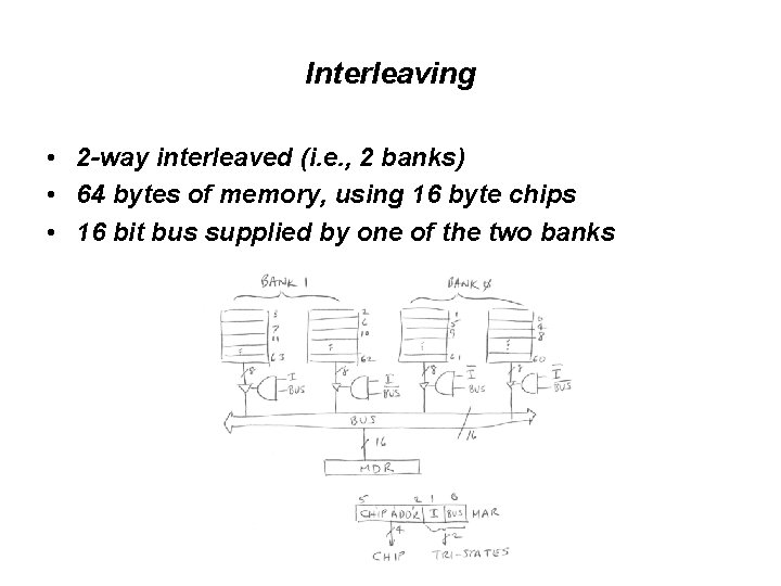
Interleaving • 2 -way interleaved (i. e. , 2 banks) • 64 bytes of memory, using 16 byte chips • 16 bit bus supplied by one of the two banks

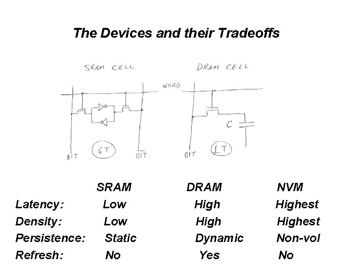
The Devices and their Tradeoffs SRAM Latency: Low Density: Low Persistence: Static Refresh: No DRAM High Dynamic Yes NVM Highest Non-vol No

The DRAM Array

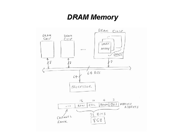
DRAM Memory

The Memory Controller • Determines which access to initiate – Bank information – Row buffer open/closed, last access R/W – Demand vs Prefetch • One per channel • Between the core and the DRAMs

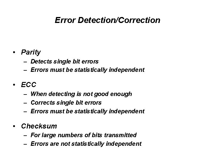
Error Detection/Correction • Parity – Detects single bit errors – Errors must be statistically independent • ECC – When detecting is not good enough – Corrects single bit errors – Errors must be statistically independent • Checksum – For large numbers of bits transmitted – Errors are not statistically independent

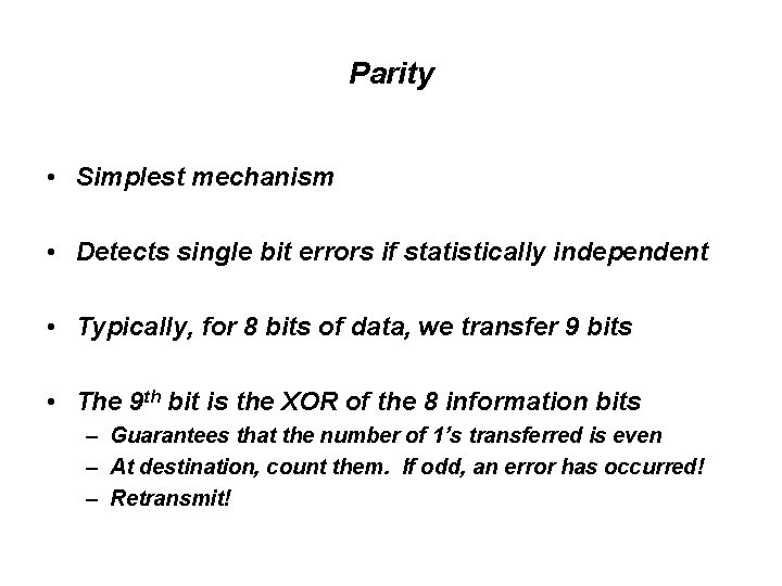
Parity • Simplest mechanism • Detects single bit errors if statistically independent • Typically, for 8 bits of data, we transfer 9 bits • The 9 th bit is the XOR of the 8 information bits – Guarantees that the number of 1’s transferred is even – At destination, count them. If odd, an error has occurred! – Retransmit!

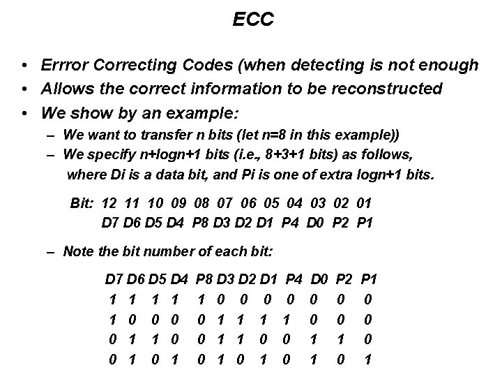
ECC • Errror Correcting Codes (when detecting is not enough • Allows the correct information to be reconstructed • We show by an example: – We want to transfer n bits (let n=8 in this example)) – We specify n+logn+1 bits (i. e. , 8+3+1 bits) as follows, where Di is a data bit, and Pi is one of extra logn+1 bits. Bit: 12 11 10 09 08 07 06 05 04 03 02 01 D 7 D 6 D 5 D 4 P 8 D 3 D 2 D 1 P 4 D 0 P 2 P 1 – Note the bit number of each bit: D 7 D 6 D 5 D 4 1 1 1 0 0 1 P 8 D 3 D 2 D 1 1 0 0 1 P 4 0 1 0 0 D 0 0 0 1 1 P 2 0 0 1 0 P 1 0 0 0 1

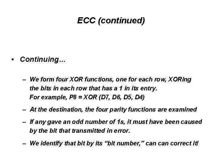
ECC (continued) • Continuing… – We form four XOR functions, one for each row, XORing the bits in each row that has a 1 in its entry. For example, P 8 = XOR (D 7, D 6, D 5, D 4) – At the destination, the four parity functions are examined – If any gave an odd number of 1 s, it must have been caused by the bit that transmitted in error. – We identify that bit by its “bit number, ” can correct it!

Checksum • When the probability of error is not statistically independent • and there is likely to be a burst of bits in error • Original scheme: use a linear feedback shift register – – – Input bit-serial the information to be transferred Output the bits from the shift register After the input has been output, output the content of LFSR At the destination, repeat the process If an error occurred, it will show up in the LFSR

Todah!