Computer Architecture Lecture 5 DRAM Operation Memory Control







![Ramulator: A Fast and Extensible DRAM Simulator [IEEE Comp Arch Letters’ 15] 84 Ramulator: A Fast and Extensible DRAM Simulator [IEEE Comp Arch Letters’ 15] 84](https://slidetodoc.com/presentation_image/543a808a2d6b1c173e05cf2e402ed7ec/image-84.jpg)
![Commodity DRAM vs. TL-DRAM [HPCA 2013] • DRAM Latency (t. RC) • DRAM Power Commodity DRAM vs. TL-DRAM [HPCA 2013] • DRAM Latency (t. RC) • DRAM Power](https://slidetodoc.com/presentation_image/543a808a2d6b1c173e05cf2e402ed7ec/image-116.jpg)


![Adaptive-Latency DRAM [HPCA 2015] n Idea: Optimize DRAM timing for the common case q Adaptive-Latency DRAM [HPCA 2015] n Idea: Optimize DRAM timing for the common case q](https://slidetodoc.com/presentation_image/543a808a2d6b1c173e05cf2e402ed7ec/image-141.jpg)

- Slides: 168

Computer Architecture Lecture 5: DRAM Operation, Memory Control & Memory Latency Prof. Onur Mutlu ETH Zürich Fall 2017 4 October 2017

High-Level Summary of Last Lecture n n n Enabling High Bandwidth Memories Main Memory System: A Broad Perspective DRAM Fundamentals and Operation 2

Agenda for Today n n n DRAM Operation Continued Memory Controllers Memory Latency 3

Lab 1 is Out n Data Cache n Implement a Data Cache in a Pipelined Processor n A lot of extra credit opportunity. n It should be a lot of fun. n Due 18 October. 4

The Main Memory System and DRAM

Required Readings on DRAM Organization and Operation Basics Sections 1 and 2 of: Lee et al. , “Tiered-Latency DRAM: A Low Latency and Low Cost DRAM Architecture, ” HPCA 2013. https: //people. inf. ethz. ch/omutlu/pub/tldram_hpca 13. pdf q Sections 1 and 2 of Kim et al. , “A Case for Subarray-Level Parallelism (SALP) in DRAM, ” ISCA 2012. https: //people. inf. ethz. ch/omutlu/pub/salp-dram_isca 12. pdf q n DRAM Refresh Basics q Sections 1 and 2 of Liu et al. , “RAIDR: Retention-Aware Intelligent DRAM Refresh, ” ISCA 2012. https: //people. inf. ethz. ch/omutlu/pub/raidr-dramrefresh_isca 12. pdf 6

Reading on Simulating Main Memory n n n How to evaluate future main memory systems? An open-source simulator and its brief description Yoongu Kim, Weikun Yang, and Onur Mutlu, "Ramulator: A Fast and Extensible DRAM Simulator" IEEE Computer Architecture Letters (CAL), March 2015. [Source Code] 7

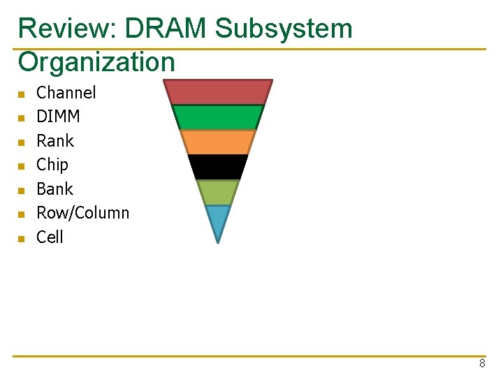
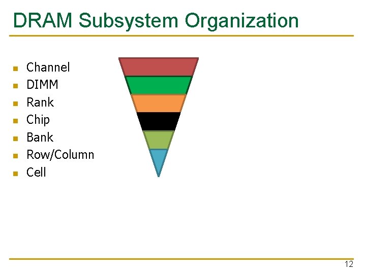
Review: DRAM Subsystem Organization n n n Channel DIMM Rank Chip Bank Row/Column Cell 8

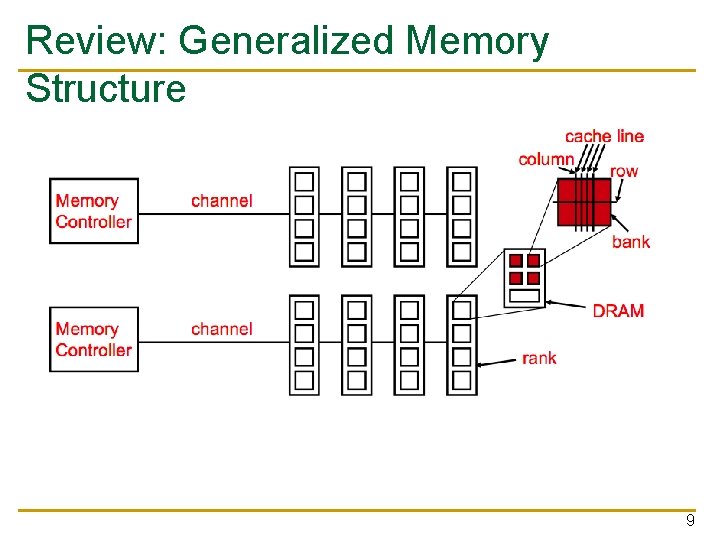
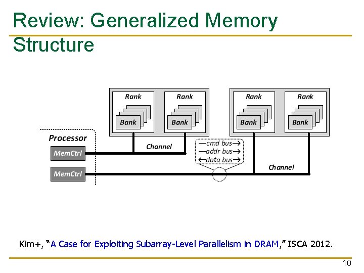
Review: Generalized Memory Structure 9

Review: Generalized Memory Structure Kim+, “A Case for Exploiting Subarray-Level Parallelism in DRAM, ” ISCA 2012. 10

The DRAM Subsystem The Top Down View

DRAM Subsystem Organization n n n Channel DIMM Rank Chip Bank Row/Column Cell 12

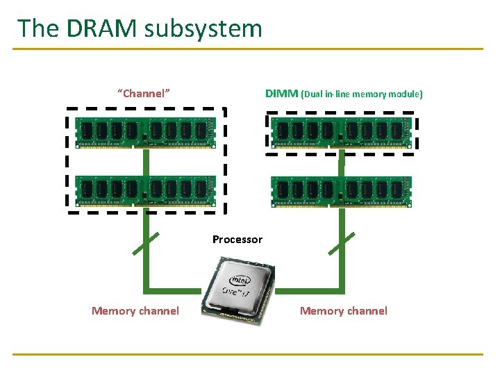
The DRAM subsystem “Channel” DIMM (Dual in-line memory module) Processor Memory channel

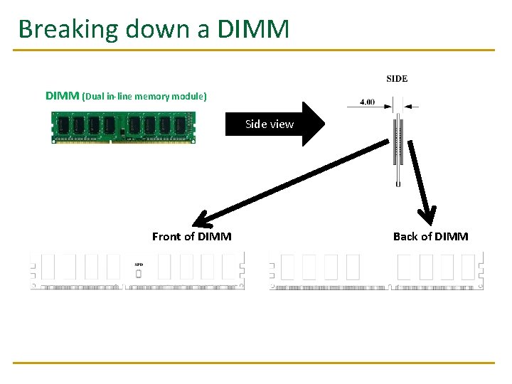
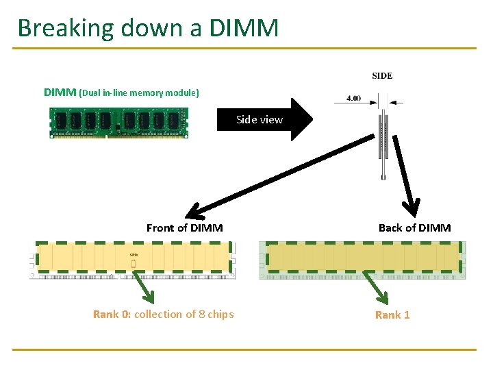
Breaking down a DIMM (Dual in-line memory module) Side view Front of DIMM Back of DIMM

Breaking down a DIMM (Dual in-line memory module) Side view Front of DIMM Rank 0: collection of 8 chips Back of DIMM Rank 1

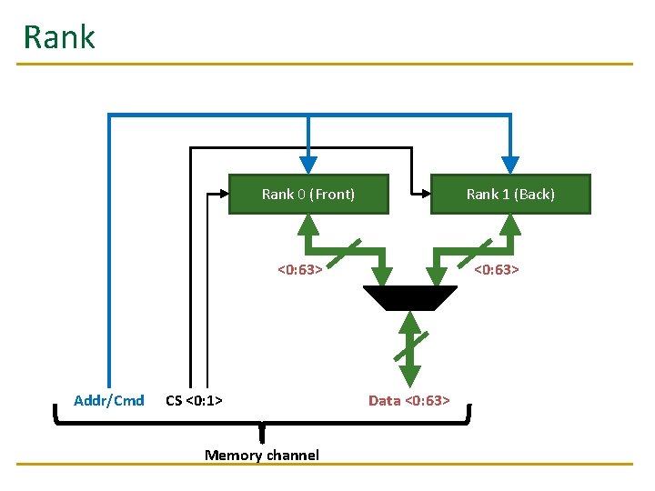
Rank 0 (Front) Rank 1 (Back) <0: 63> Addr/Cmd CS <0: 1> Memory channel <0: 63> Data <0: 63>

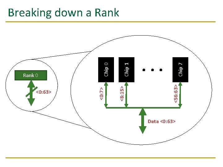
Chip 7 . . . <56: 63> Chip 1 <8: 15> <0: 63> <0: 7> Rank 0 Chip 0 Breaking down a Rank Data <0: 63>

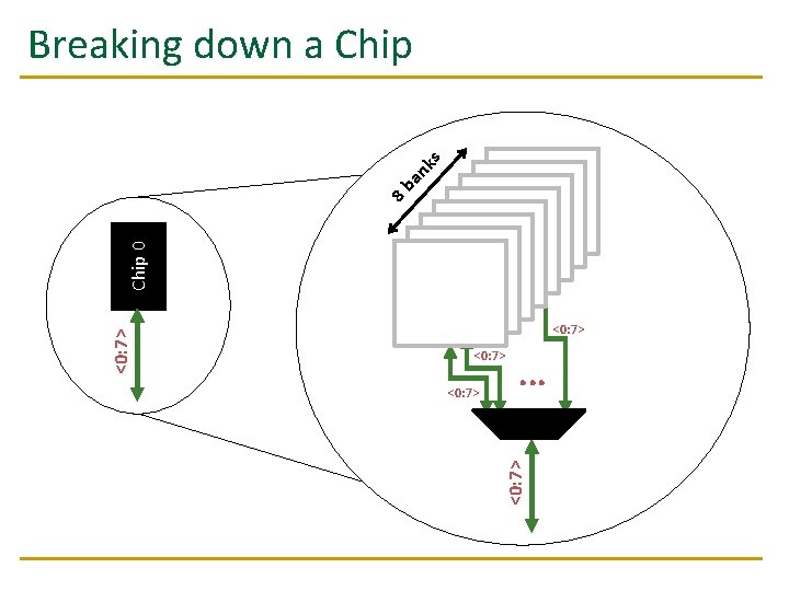
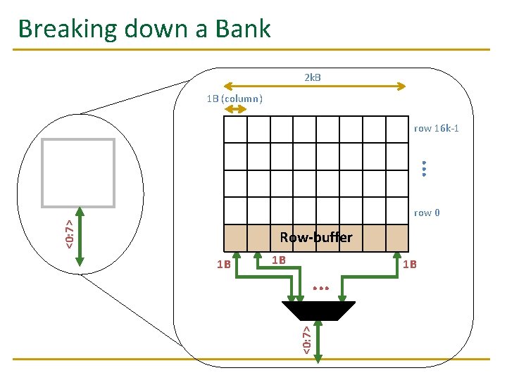
Bank 0 <0: 7> . . . <0: 7> Chip 0 8 b an ks Breaking down a Chip

Breaking down a Bank 2 k. B 1 B (column) row 16 k-1 . . . Bank 0 <0: 7> row 0 Row-buffer 1 B . . . <0: 7> 1 B 1 B

DRAM Subsystem Organization n n n Channel DIMM Rank Chip Bank Row/Column Cell 20

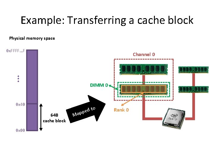
Example: Transferring a cache block Physical memory space 0 x. FFFF…F . . . Channel 0 DIMM 0 0 x 40 64 B cache block 0 x 00 to d e p Map Rank 0

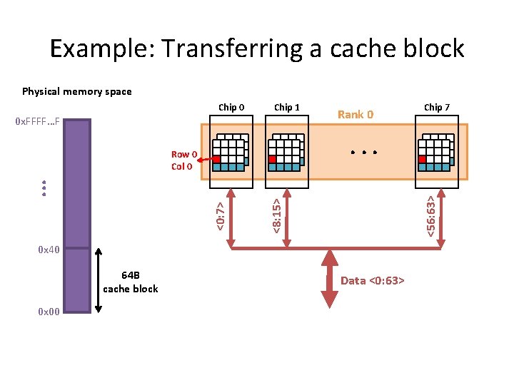
Example: Transferring a cache block Physical memory space Chip 0 Chip 1 0 x. FFFF…F Rank 0 Chip 7 <56: 63> <8: 15> <0: 7> . . . 0 x 40 64 B cache block 0 x 00 Data <0: 63>

Example: Transferring a cache block Physical memory space Chip 0 Chip 1 0 x. FFFF…F Rank 0 . . . <56: 63> <8: 15> <0: 7> . . . Row 0 Col 0 0 x 40 64 B cache block 0 x 00 Chip 7 Data <0: 63>

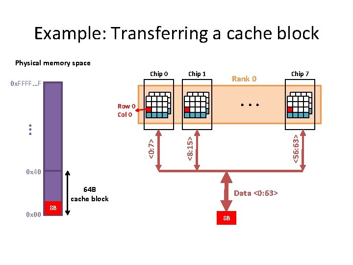
Example: Transferring a cache block Physical memory space Chip 0 Chip 1 Rank 0 0 x. FFFF…F . . . <56: 63> <8: 15> <0: 7> . . . Row 0 Col 0 0 x 40 64 B cache block 0 x 00 Chip 7 Data <0: 63> 8 B 8 B

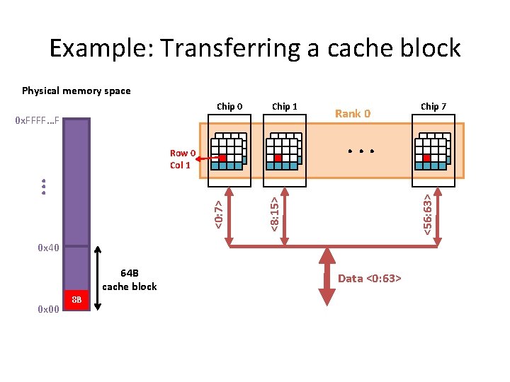
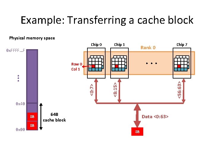
Example: Transferring a cache block Physical memory space Chip 0 Chip 1 0 x. FFFF…F Rank 0 . . . <56: 63> <8: 15> <0: 7> . . . Row 0 Col 1 0 x 40 64 B cache block 0 x 00 8 B Chip 7 Data <0: 63>

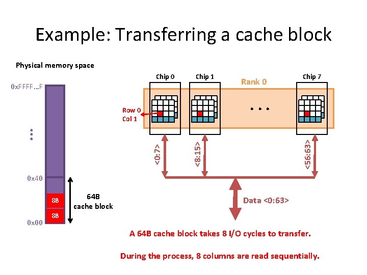
Example: Transferring a cache block Physical memory space Chip 0 Chip 1 Rank 0 0 x. FFFF…F . . . <56: 63> <8: 15> <0: 7> . . . Row 0 Col 1 0 x 40 8 B 0 x 00 Chip 7 64 B cache block Data <0: 63> 8 B 8 B

Example: Transferring a cache block Physical memory space Chip 0 Chip 1 0 x. FFFF…F Rank 0 Chip 7 . . . <56: 63> <8: 15> <0: 7> . . . Row 0 Col 1 0 x 40 8 B 0 x 00 64 B cache block Data <0: 63> 8 B A 64 B cache block takes 8 I/O cycles to transfer. During the process, 8 columns are read sequentially.

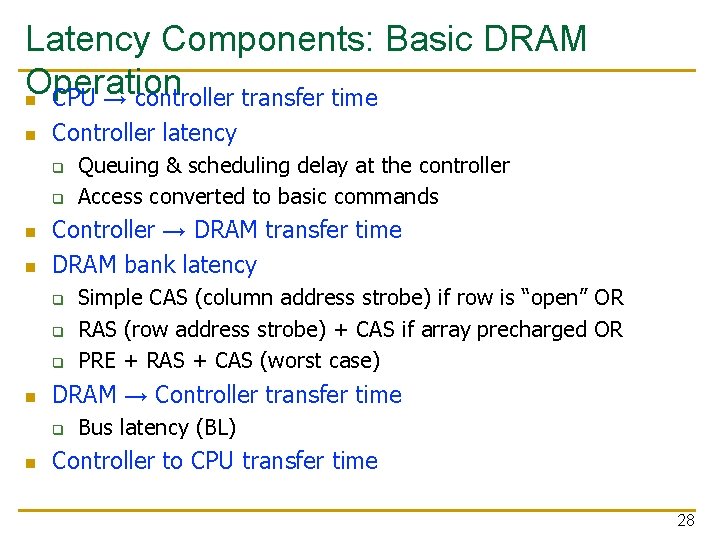
Latency Components: Basic DRAM Operation n CPU → controller transfer time n Controller latency q q n n Controller → DRAM transfer time DRAM bank latency q q q n Simple CAS (column address strobe) if row is “open” OR RAS (row address strobe) + CAS if array precharged OR PRE + RAS + CAS (worst case) DRAM → Controller transfer time q n Queuing & scheduling delay at the controller Access converted to basic commands Bus latency (BL) Controller to CPU transfer time 28

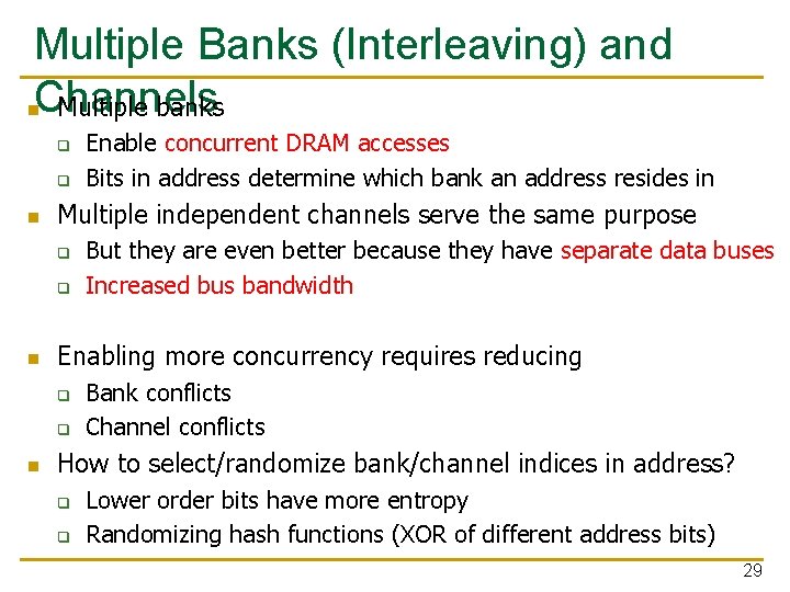
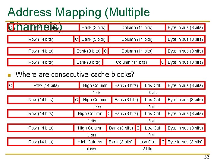
Multiple Banks (Interleaving) and n. Channels Multiple banks q q n Multiple independent channels serve the same purpose q q n But they are even better because they have separate data buses Increased bus bandwidth Enabling more concurrency requires reducing q q n Enable concurrent DRAM accesses Bits in address determine which bank an address resides in Bank conflicts Channel conflicts How to select/randomize bank/channel indices in address? q q Lower order bits have more entropy Randomizing hash functions (XOR of different address bits) 29

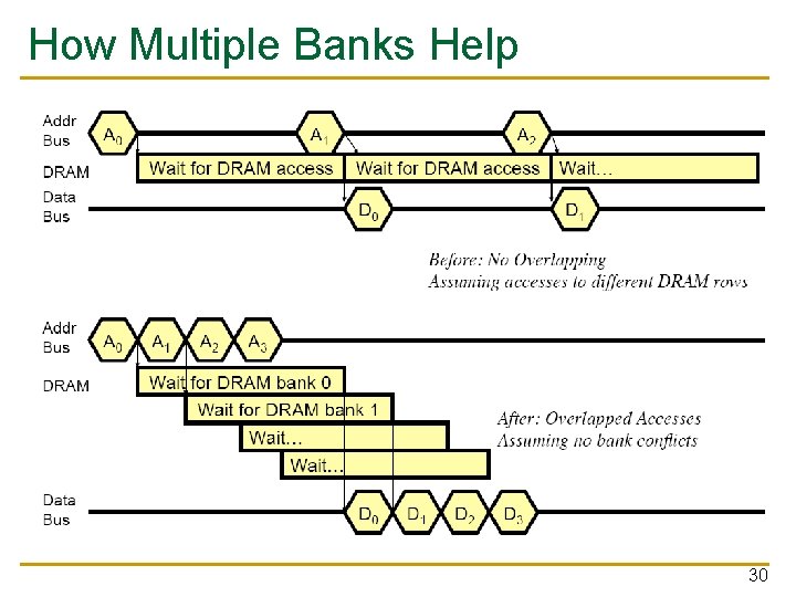
How Multiple Banks Help 30

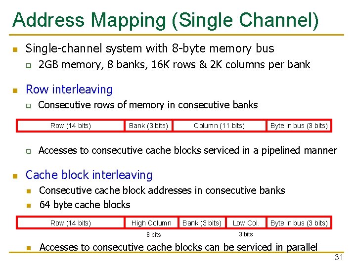
Address Mapping (Single Channel) n Single-channel system with 8 -byte memory bus q n 2 GB memory, 8 banks, 16 K rows & 2 K columns per bank Row interleaving q Consecutive rows of memory in consecutive banks Row (14 bits) q n Bank (3 bits) Column (11 bits) Byte in bus (3 bits) Accesses to consecutive cache blocks serviced in a pipelined manner Cache block interleaving n n Consecutive cache block addresses in consecutive banks 64 byte cache blocks Row (14 bits) High Column 8 bits n Bank (3 bits) Low Col. Byte in bus (3 bits) 3 bits Accesses to consecutive cache blocks can be serviced in parallel 31

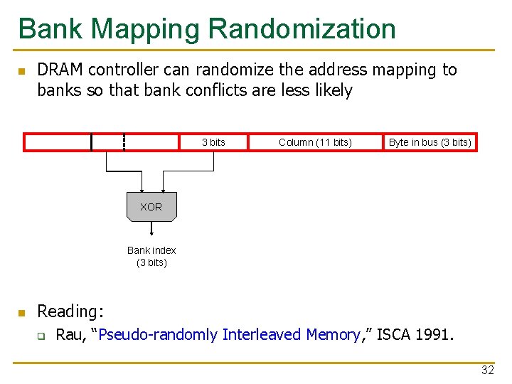
Bank Mapping Randomization n DRAM controller can randomize the address mapping to banks so that bank conflicts are less likely 3 bits Column (11 bits) Byte in bus (3 bits) XOR Bank index (3 bits) n Reading: q Rau, “Pseudo-randomly Interleaved Memory, ” ISCA 1991. 32

Address Mapping (Multiple Channels) C Row (14 bits) n C Bank (3 bits) Column (11 bits) Byte in bus (3 bits) Row (14 bits) Bank (3 bits) Column (11 bits) C Byte in bus (3 bits) Where are consecutive cache blocks? Row (14 bits) High Column Bank (3 bits) Low Col. 3 bits 8 bits Row (14 bits) C High Column Bank (3 bits) Low Col. High Column C Bank (3 bits) Low Col. High Column Bank (3 bits) C High Column 8 bits Low Col. Byte in bus (3 bits) 3 bits 8 bits Row (14 bits) Byte in bus (3 bits) Bank (3 bits) Low Col. C Byte in bus (3 bits) 3 bits 33

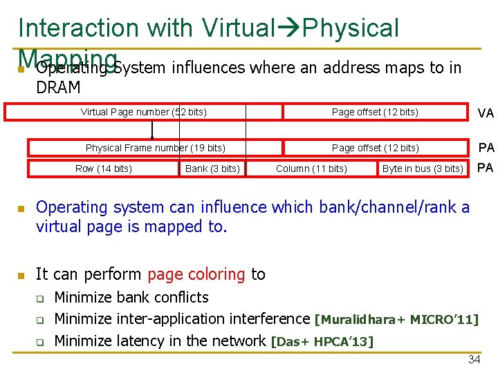
Interaction with Virtual Physical Mapping n Operating System influences where an address maps to in DRAM Virtual Page number (52 bits) Physical Frame number (19 bits) Row (14 bits) n n Bank (3 bits) Page offset (12 bits) VA Page offset (12 bits) PA Column (11 bits) PA Byte in bus (3 bits) Operating system can influence which bank/channel/rank a virtual page is mapped to. It can perform page coloring to q q q Minimize bank conflicts Minimize inter-application interference [Muralidhara+ MICRO’ 11] Minimize latency in the network [Das+ HPCA’ 13] 34

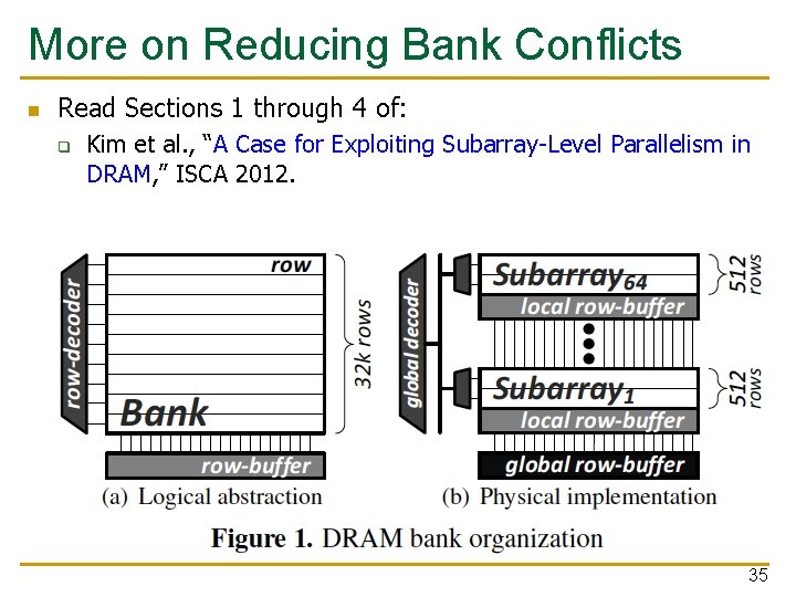
More on Reducing Bank Conflicts n Read Sections 1 through 4 of: q Kim et al. , “A Case for Exploiting Subarray-Level Parallelism in DRAM, ” ISCA 2012. 35

Required Reading on DRAM n Yoongu Kim, Vivek Seshadri, Donghyuk Lee, Jamie Liu, and Onur Mutlu, "A Case for Exploiting Subarray-Level Parallelism (SALP) in DRAM" Proceedings of the 39 th International Symposium on Computer Architecture (ISCA), Portland, OR, June 2012. Slides (pptx) n Sections 1 -2 are required 36

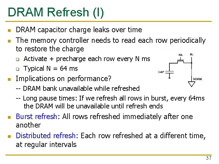
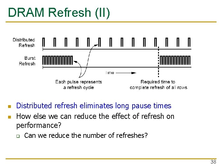
DRAM Refresh (I) n n DRAM capacitor charge leaks over time The memory controller needs to read each row periodically to restore the charge q q n Activate + precharge each row every N ms Typical N = 64 ms Implications on performance? -- DRAM bank unavailable while refreshed -- Long pause times: If we refresh all rows in burst, every 64 ms the DRAM will be unavailable until refresh ends n n Burst refresh: All rows refreshed immediately after one another Distributed refresh: Each row refreshed at a different time, at regular intervals 37

DRAM Refresh (II) n n Distributed refresh eliminates long pause times How else we can reduce the effect of refresh on performance? q Can we reduce the number of refreshes? 38

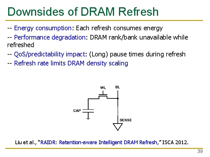
Downsides of DRAM Refresh -- Energy consumption: Each refresh consumes energy -- Performance degradation: DRAM rank/bank unavailable while refreshed -- Qo. S/predictability impact: (Long) pause times during refresh -- Refresh rate limits DRAM density scaling Liu et al. , “RAIDR: Retention-aware Intelligent DRAM Refresh, ” ISCA 2012. 39

Memory Controllers

DRAM versus Other Types of Memories n n Long latency memories have similar characteristics that need to be controlled. The following discussion will use DRAM as an example, but many scheduling and control issues are similar in the design of controllers for other types of memories q q Flash memory Other emerging memory technologies n n q Phase Change Memory Spin-Transfer Torque Magnetic Memory These other technologies can place other demands on the controller 41

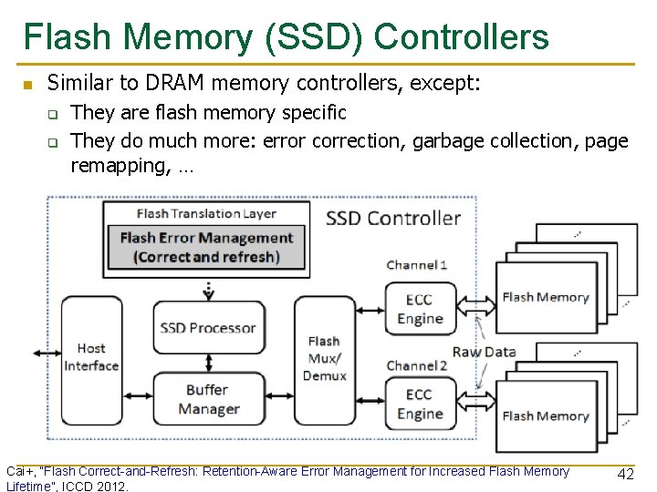
Flash Memory (SSD) Controllers n Similar to DRAM memory controllers, except: q q They are flash memory specific They do much more: error correction, garbage collection, page remapping, … Cai+, “Flash Correct-and-Refresh: Retention-Aware Error Management for Increased Flash Memory Lifetime”, ICCD 2012. 42

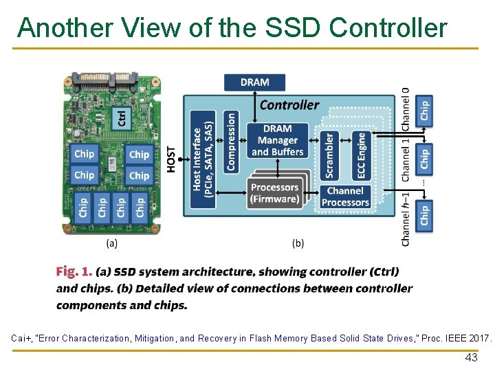
Another View of the SSD Controller Cai+, “Error Characterization, Mitigation, and Recovery in Flash Memory Based Solid State Drives, ” Proc. IEEE 2017. 43

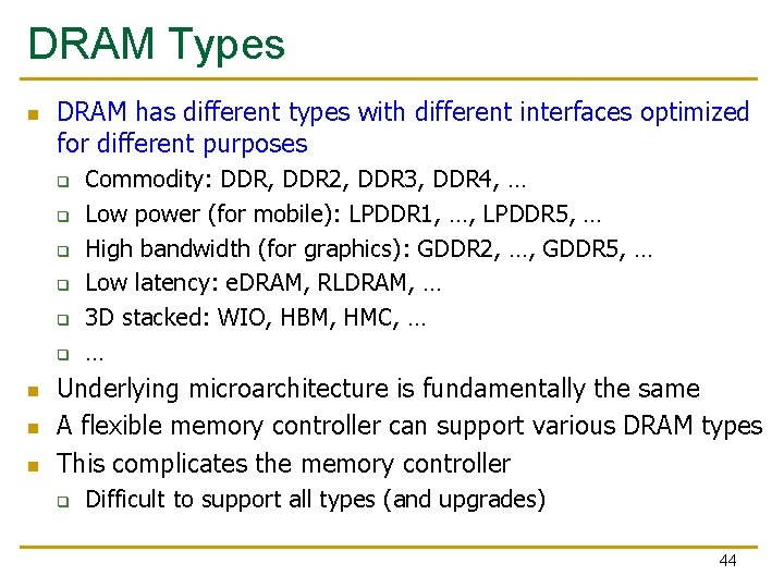
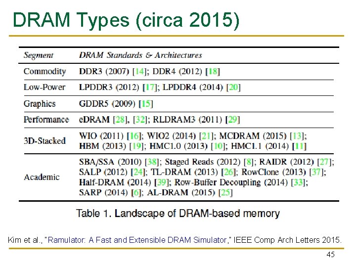
DRAM Types n DRAM has different types with different interfaces optimized for different purposes q q q n n n Commodity: DDR, DDR 2, DDR 3, DDR 4, … Low power (for mobile): LPDDR 1, …, LPDDR 5, … High bandwidth (for graphics): GDDR 2, …, GDDR 5, … Low latency: e. DRAM, RLDRAM, … 3 D stacked: WIO, HBM, HMC, … … Underlying microarchitecture is fundamentally the same A flexible memory controller can support various DRAM types This complicates the memory controller q Difficult to support all types (and upgrades) 44

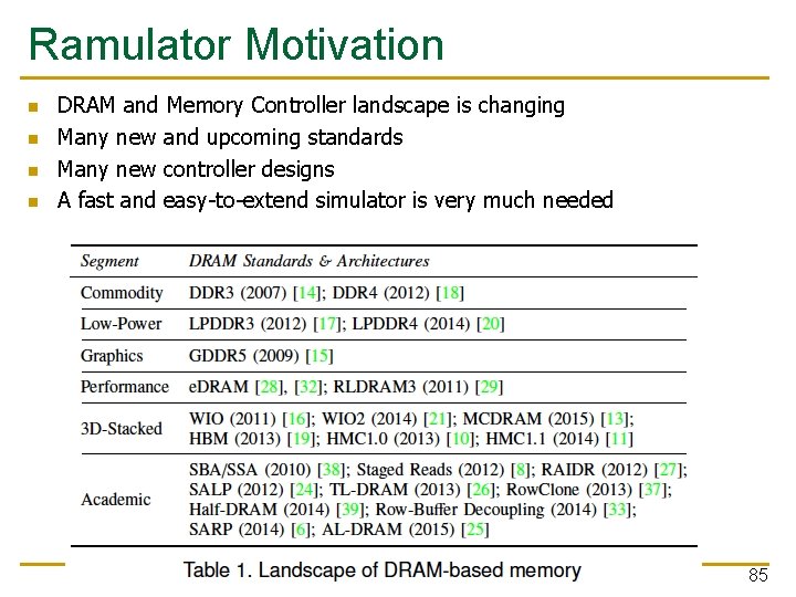
DRAM Types (circa 2015) Kim et al. , “Ramulator: A Fast and Extensible DRAM Simulator, ” IEEE Comp Arch Letters 2015. 45

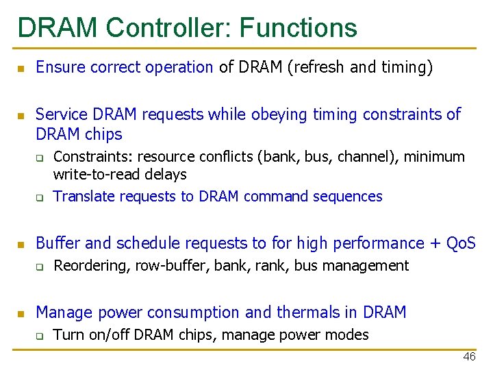
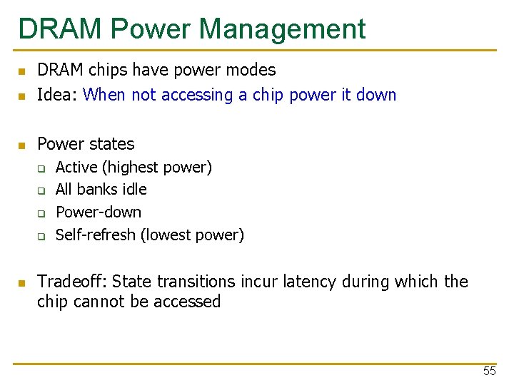
DRAM Controller: Functions n n Ensure correct operation of DRAM (refresh and timing) Service DRAM requests while obeying timing constraints of DRAM chips q q n Buffer and schedule requests to for high performance + Qo. S q n Constraints: resource conflicts (bank, bus, channel), minimum write-to-read delays Translate requests to DRAM command sequences Reordering, row-buffer, bank, rank, bus management Manage power consumption and thermals in DRAM q Turn on/off DRAM chips, manage power modes 46

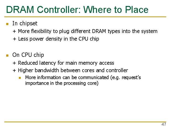
DRAM Controller: Where to Place n In chipset + More flexibility to plug different DRAM types into the system + Less power density in the CPU chip n On CPU chip + Reduced latency for main memory access + Higher bandwidth between cores and controller n More information can be communicated (e. g. request’s importance in the processing core) 47

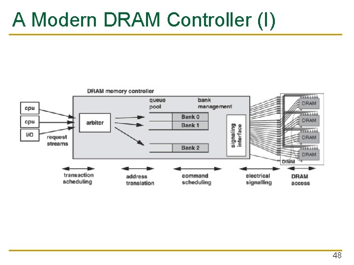
A Modern DRAM Controller (I) 48

A Modern DRAM Controller 49

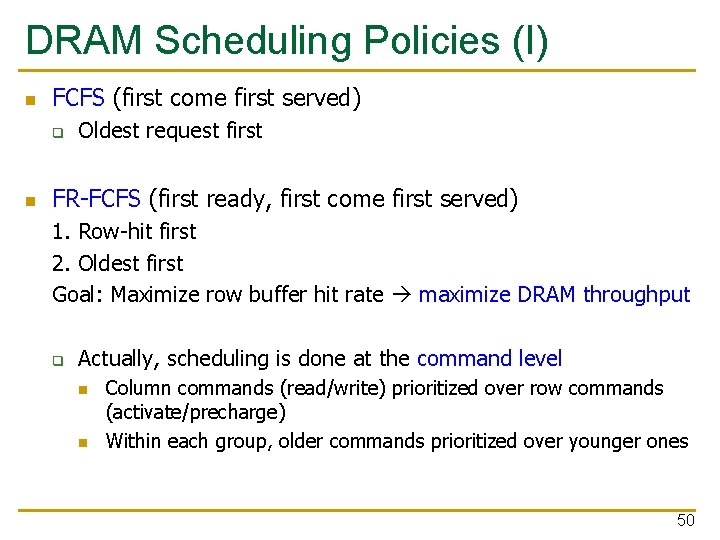
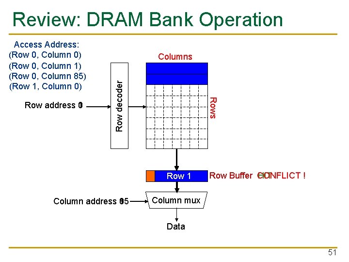
DRAM Scheduling Policies (I) n FCFS (first come first served) q n Oldest request first FR-FCFS (first ready, first come first served) 1. Row-hit first 2. Oldest first Goal: Maximize row buffer hit rate maximize DRAM throughput q Actually, scheduling is done at the command level n n Column commands (read/write) prioritized over row commands (activate/precharge) Within each group, older commands prioritized over younger ones 50

Review: DRAM Bank Operation Rows Row address 0 Row address 1 Columns Row decoder Access Address: (Row 0, Column 0) (Row 0, Column 1) (Row 0, Column 85) (Row 1, Column 0) Row 1 Row 0 Empty Column address 0 Column address 1 Column address 85 Row Buffer CONFLICT ! HIT Column mux Data 51

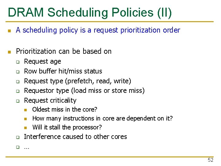
DRAM Scheduling Policies (II) n A scheduling policy is a request prioritization order n Prioritization can be based on q q q Request age Row buffer hit/miss status Request type (prefetch, read, write) Requestor type (load miss or store miss) Request criticality n n n q q Oldest miss in the core? How many instructions in core are dependent on it? Will it stall the processor? Interference caused to other cores … 52

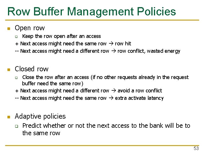
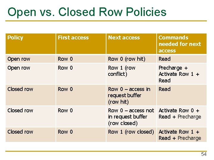
Row Buffer Management Policies n Open row Keep the row open after an access + Next access might need the same row hit -- Next access might need a different row conflict, wasted energy q n Closed row Close the row after an access (if no other requests already in the request buffer need the same row) + Next access might need a different row avoid a row conflict -- Next access might need the same row extra activate latency q n Adaptive policies q Predict whether or not the next access to the bank will be to the same row 53

Open vs. Closed Row Policies Policy First access Next access Commands needed for next access Open row Row 0 (row hit) Read Open row Row 0 Row 1 (row conflict) Precharge + Activate Row 1 + Read Closed row Row 0 – access in request buffer (row hit) Read Closed row Row 0 – access not Activate Row 0 + in request buffer Read + Precharge (row closed) Closed row Row 0 Row 1 (row closed) Activate Row 1 + Read + Precharge 54

DRAM Power Management n DRAM chips have power modes Idea: When not accessing a chip power it down n Power states n q q n Active (highest power) All banks idle Power-down Self-refresh (lowest power) Tradeoff: State transitions incur latency during which the chip cannot be accessed 55

Difficulty of DRAM Control

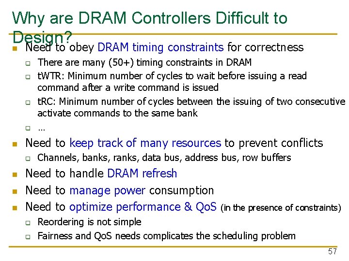
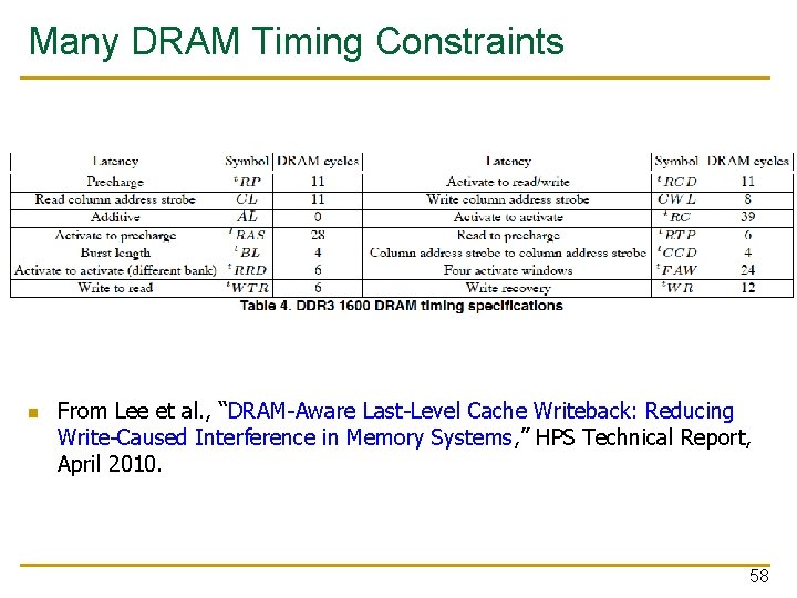
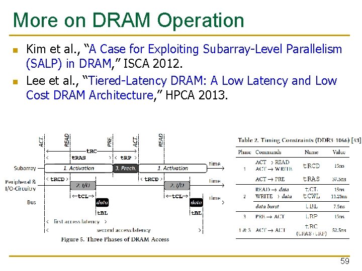
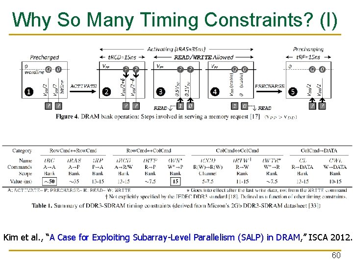
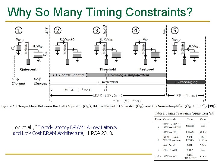
Why are DRAM Controllers Difficult to Design? n Need to obey DRAM timing constraints for correctness q q n Need to keep track of many resources to prevent conflicts q n n n There are many (50+) timing constraints in DRAM t. WTR: Minimum number of cycles to wait before issuing a read command after a write command is issued t. RC: Minimum number of cycles between the issuing of two consecutive activate commands to the same bank … Channels, banks, ranks, data bus, address bus, row buffers Need to handle DRAM refresh Need to manage power consumption Need to optimize performance & Qo. S (in the presence of constraints) q q Reordering is not simple Fairness and Qo. S needs complicates the scheduling problem 57

Many DRAM Timing Constraints n From Lee et al. , “DRAM-Aware Last-Level Cache Writeback: Reducing Write-Caused Interference in Memory Systems, ” HPS Technical Report, April 2010. 58

More on DRAM Operation n n Kim et al. , “A Case for Exploiting Subarray-Level Parallelism (SALP) in DRAM, ” ISCA 2012. Lee et al. , “Tiered-Latency DRAM: A Low Latency and Low Cost DRAM Architecture, ” HPCA 2013. 59

Why So Many Timing Constraints? (I) Kim et al. , “A Case for Exploiting Subarray-Level Parallelism (SALP) in DRAM, ” ISCA 2012. 60

Why So Many Timing Constraints? (II) Lee et al. , “Tiered-Latency DRAM: A Low Latency and Low Cost DRAM Architecture, ” HPCA 2013. 61

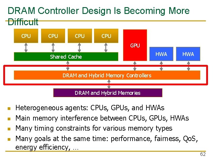
DRAM Controller Design Is Becoming More Difficult CPU CPU GPU Shared Cache HWA DRAM and Hybrid Memory Controllers DRAM and Hybrid Memories n n Heterogeneous agents: CPUs, GPUs, and HWAs Main memory interference between CPUs, GPUs, HWAs Many timing constraints for various memory types Many goals at the same time: performance, fairness, Qo. S, energy efficiency, … 62

Reality and Dream n n Reality: It difficult to optimize all these different constraints while maximizing performance, Qo. S, energy-efficiency, … Dream: Wouldn’t it be nice if the DRAM controller automatically found a good scheduling policy on its own? 63

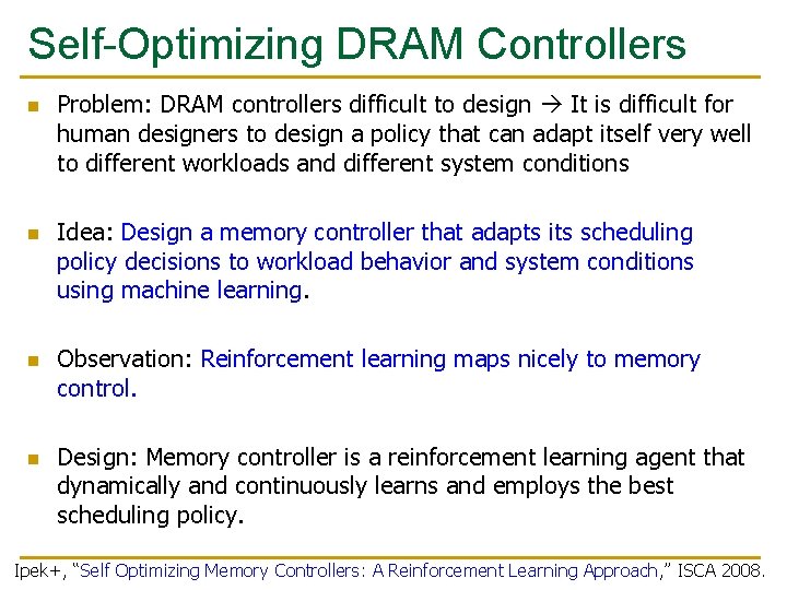
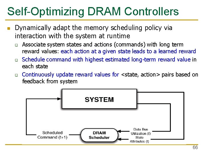
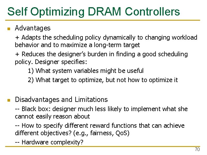
Self-Optimizing DRAM Controllers n n Problem: DRAM controllers difficult to design It is difficult for human designers to design a policy that can adapt itself very well to different workloads and different system conditions Idea: Design a memory controller that adapts its scheduling policy decisions to workload behavior and system conditions using machine learning. Observation: Reinforcement learning maps nicely to memory control. Design: Memory controller is a reinforcement learning agent that dynamically and continuously learns and employs the best scheduling policy. Ipek+, “Self Optimizing Memory Controllers: A Reinforcement Learning Approach, ” ISCA 2008.

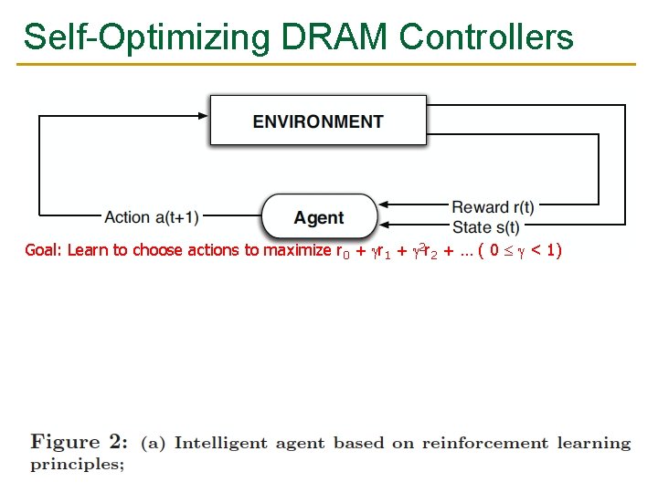
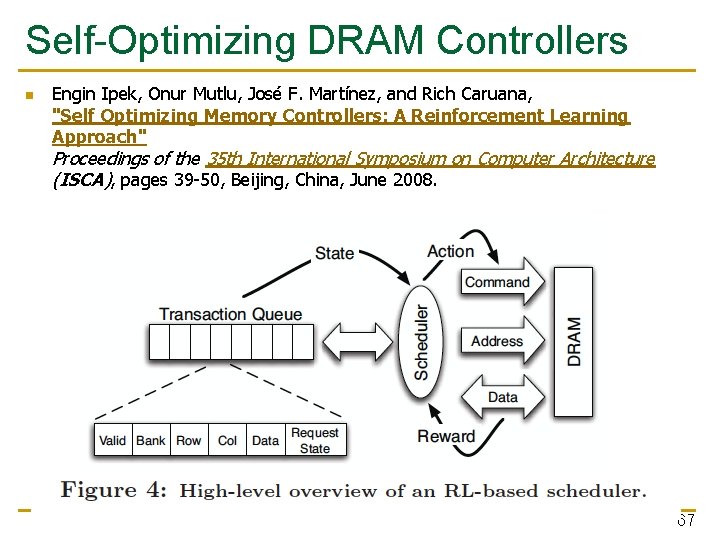
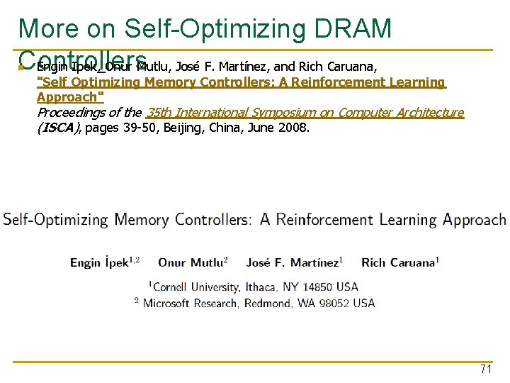
Self-Optimizing DRAM Controllers n Engin Ipek, Onur Mutlu, José F. Martínez, and Rich Caruana, "Self Optimizing Memory Controllers: A Reinforcement Learning Approach" Proceedings of the 35 th International Symposium on Computer Architecture (ISCA), pages 39 -50, Beijing, China, 2 June 2008. Goal: Learn to choose actions to maximize r 0 + r 1 + r 2 + … ( 0 < 1) 65

Self-Optimizing DRAM Controllers n Dynamically adapt the memory scheduling policy via interaction with the system at runtime q q q Associate system states and actions (commands) with long term reward values: each action at a given state leads to a learned reward Schedule command with highest estimated long-term reward value in each state Continuously update reward values for <state, action> pairs based on feedback from system 66

Self-Optimizing DRAM Controllers n Engin Ipek, Onur Mutlu, José F. Martínez, and Rich Caruana, "Self Optimizing Memory Controllers: A Reinforcement Learning Approach" Proceedings of the 35 th International Symposium on Computer Architecture (ISCA), pages 39 -50, Beijing, China, June 2008. 67

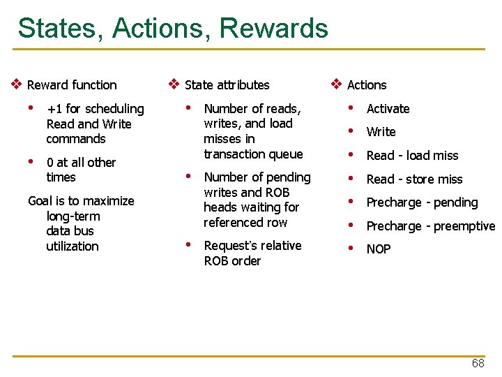
States, Actions, Rewards ❖ Reward function • +1 for scheduling Read and Write commands • ❖ State attributes • Number of reads, writes, and load misses in transaction queue 0 at all other times • Goal is to maximize long-term data bus utilization Number of pending writes and ROB heads waiting for referenced row • Request’s relative ROB order ❖ Actions • Activate • Write • Read - load miss • Read - store miss • Precharge - pending • Precharge - preemptive • NOP 68

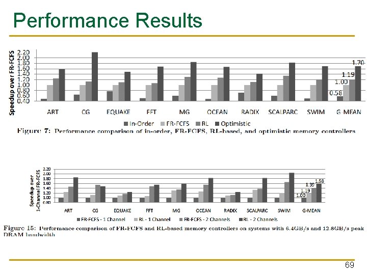
Performance Results 69

Self Optimizing DRAM Controllers n Advantages + Adapts the scheduling policy dynamically to changing workload behavior and to maximize a long-term target + Reduces the designer’s burden in finding a good scheduling policy. Designer specifies: 1) What system variables might be useful 2) What target to optimize, but not how to optimize it n Disadvantages and Limitations -- Black box: designer much less likely to implement what she cannot easily reason about -- How to specify different reward functions that can achieve different objectives? (e. g. , fairness, Qo. S) -- Hardware complexity? 70

More on Self-Optimizing DRAM Controllers Engin Ipek, Onur Mutlu, José F. Martínez, and Rich Caruana, n "Self Optimizing Memory Controllers: A Reinforcement Learning Approach" Proceedings of the 35 th International Symposium on Computer Architecture (ISCA), pages 39 -50, Beijing, China, June 2008. 71

Evaluating New Ideas for New (Memory) Architectures

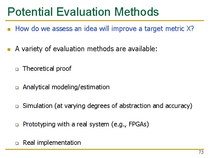
Potential Evaluation Methods n How do we assess an idea will improve a target metric X? n A variety of evaluation methods are available: q Theoretical proof q Analytical modeling/estimation q Simulation (at varying degrees of abstraction and accuracy) q Prototyping with a real system (e. g. , FPGAs) q Real implementation 73

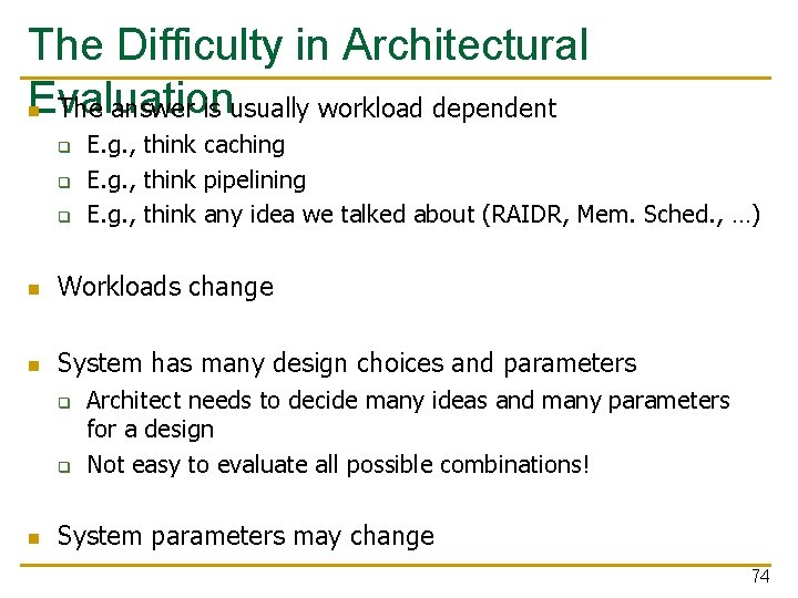
The Difficulty in Architectural Evaluation n The answer is usually workload dependent q q q E. g. , think caching E. g. , think pipelining E. g. , think any idea we talked about (RAIDR, Mem. Sched. , …) n Workloads change n System has many design choices and parameters q q n Architect needs to decide many ideas and many parameters for a design Not easy to evaluate all possible combinations! System parameters may change 74

Simulation: The Field of Dreams

Dreaming and Reality n An architect is in part a dreamer, a creator n Simulation is a key tool of the architect n Simulation enables q q q n The exploration of many dreams A reality check of the dreams Deciding which dream is better Simulation also enables q The ability to fool yourself with false dreams 76

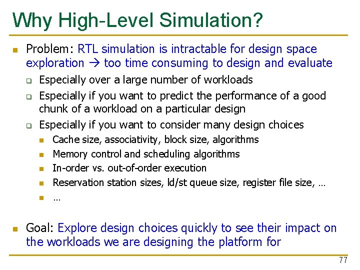
Why High-Level Simulation? n Problem: RTL simulation is intractable for design space exploration too time consuming to design and evaluate q q q Especially over a large number of workloads Especially if you want to predict the performance of a good chunk of a workload on a particular design Especially if you want to consider many design choices n n n Cache size, associativity, block size, algorithms Memory control and scheduling algorithms In-order vs. out-of-order execution Reservation station sizes, ld/st queue size, register file size, … … Goal: Explore design choices quickly to see their impact on the workloads we are designing the platform for 77

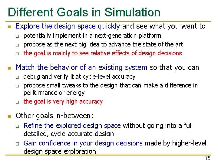
Different Goals in Simulation n Explore the design space quickly and see what you want to q q q n Match the behavior of an existing system so that you can q q q n potentially implement in a next-generation platform propose as the next big idea to advance the state of the art the goal is mainly to see relative effects of design decisions debug and verify it at cycle-level accuracy propose small tweaks to the design that can make a difference in performance or energy the goal is very high accuracy Other goals in-between: q q Refine the explored design space without going into a full detailed, cycle-accurate design Gain confidence in your design decisions made by higher-level design space exploration 78

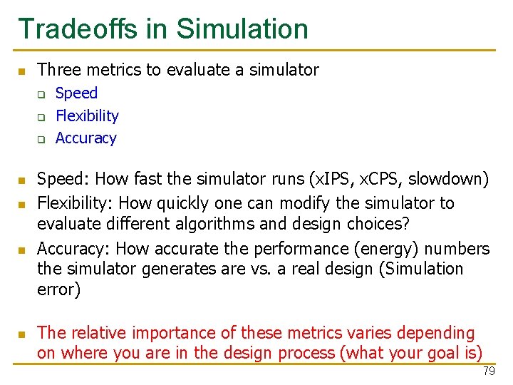
Tradeoffs in Simulation n Three metrics to evaluate a simulator q q q n n Speed Flexibility Accuracy Speed: How fast the simulator runs (x. IPS, x. CPS, slowdown) Flexibility: How quickly one can modify the simulator to evaluate different algorithms and design choices? Accuracy: How accurate the performance (energy) numbers the simulator generates are vs. a real design (Simulation error) The relative importance of these metrics varies depending on where you are in the design process (what your goal is) 79

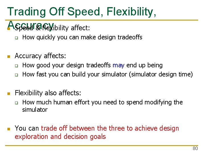
Trading Off Speed, Flexibility, Accuracy n Speed & flexibility affect: q n Accuracy affects: q q n How good your design tradeoffs may end up being How fast you can build your simulator (simulator design time) Flexibility also affects: q n How quickly you can make design tradeoffs How much human effort you need to spend modifying the simulator You can trade off between the three to achieve design exploration and decision goals 80

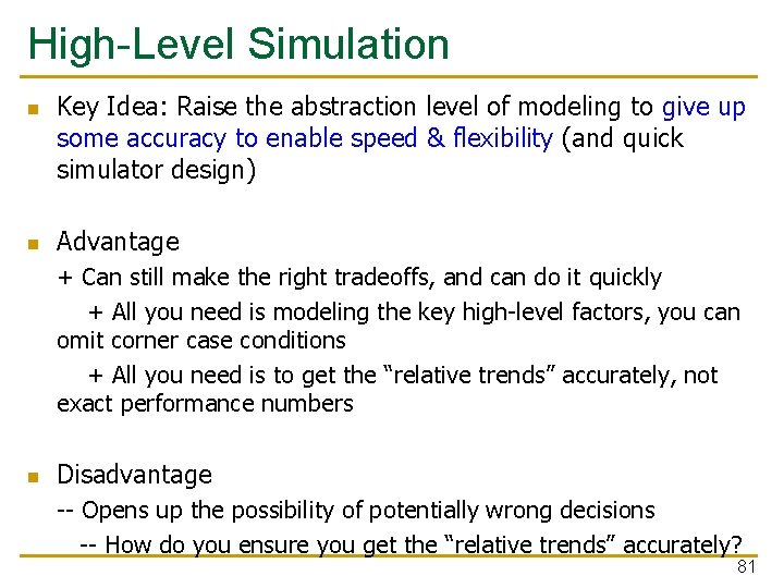
High-Level Simulation n n Key Idea: Raise the abstraction level of modeling to give up some accuracy to enable speed & flexibility (and quick simulator design) Advantage + Can still make the right tradeoffs, and can do it quickly + All you need is modeling the key high-level factors, you can omit corner case conditions + All you need is to get the “relative trends” accurately, not exact performance numbers n Disadvantage -- Opens up the possibility of potentially wrong decisions -- How do you ensure you get the “relative trends” accurately? 81

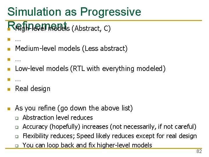
Simulation as Progressive Refinement n High-level models (Abstract, C) n … Medium-level models (Less abstract) … Low-level models (RTL with everything modeled) … Real design n As you refine (go down the above list) n n n q q Abstraction level reduces Accuracy (hopefully) increases (not necessarily, if not careful) Flexibility reduces; Speed likely reduces except for real design You can loop back and fix higher-level models 82

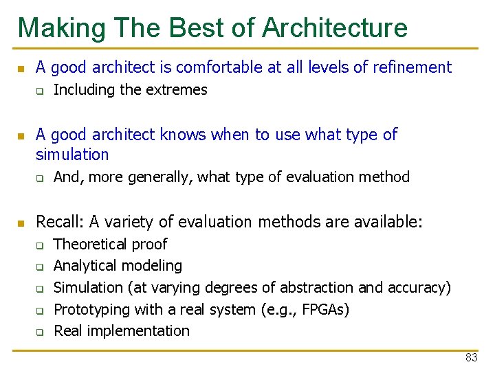
Making The Best of Architecture n A good architect is comfortable at all levels of refinement q n A good architect knows when to use what type of simulation q n Including the extremes And, more generally, what type of evaluation method Recall: A variety of evaluation methods are available: q q q Theoretical proof Analytical modeling Simulation (at varying degrees of abstraction and accuracy) Prototyping with a real system (e. g. , FPGAs) Real implementation 83
![Ramulator A Fast and Extensible DRAM Simulator IEEE Comp Arch Letters 15 84 Ramulator: A Fast and Extensible DRAM Simulator [IEEE Comp Arch Letters’ 15] 84](https://slidetodoc.com/presentation_image/543a808a2d6b1c173e05cf2e402ed7ec/image-84.jpg)
Ramulator: A Fast and Extensible DRAM Simulator [IEEE Comp Arch Letters’ 15] 84

Ramulator Motivation n n DRAM and Memory Controller landscape is changing Many new and upcoming standards Many new controller designs A fast and easy-to-extend simulator is very much needed 85

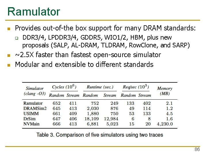
Ramulator n Provides out-of-the box support for many DRAM standards: q n n DDR 3/4, LPDDR 3/4, GDDR 5, WIO 1/2, HBM, plus new proposals (SALP, AL-DRAM, TLDRAM, Row. Clone, and SARP) ~2. 5 X faster than fastest open-source simulator Modular and extensible to different standards 86

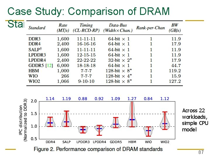
Case Study: Comparison of DRAM Standards Across 22 workloads, simple CPU model 87

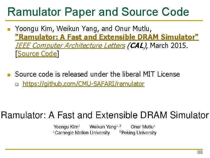
Ramulator Paper and Source Code n n Yoongu Kim, Weikun Yang, and Onur Mutlu, "Ramulator: A Fast and Extensible DRAM Simulator" IEEE Computer Architecture Letters (CAL), March 2015. [Source Code] Source code is released under the liberal MIT License q https: //github. com/CMU-SAFARI/ramulator 88

Extra Credit Assignment n Review the Ramulator paper q n Download and run Ramulator q q n Online on our review site Compare DDR 3, DDR 4, SALP, HBM for the libquantum benchmark (provided in Ramulator repository) Upload your brief report to Moodle This may become part of a future homework 89

Memory Latency: Fundamental Tradeoffs

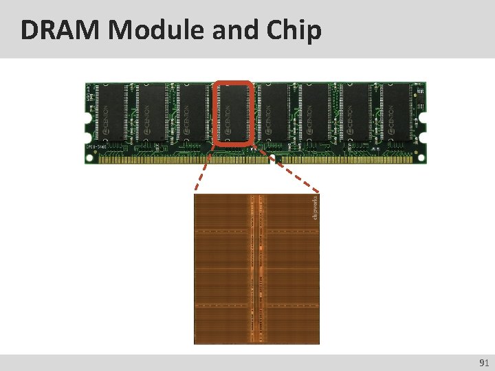
DRAM Module and Chip 91

Goals • • Cost Latency Bandwidth Parallelism Power Energy Reliability … 92

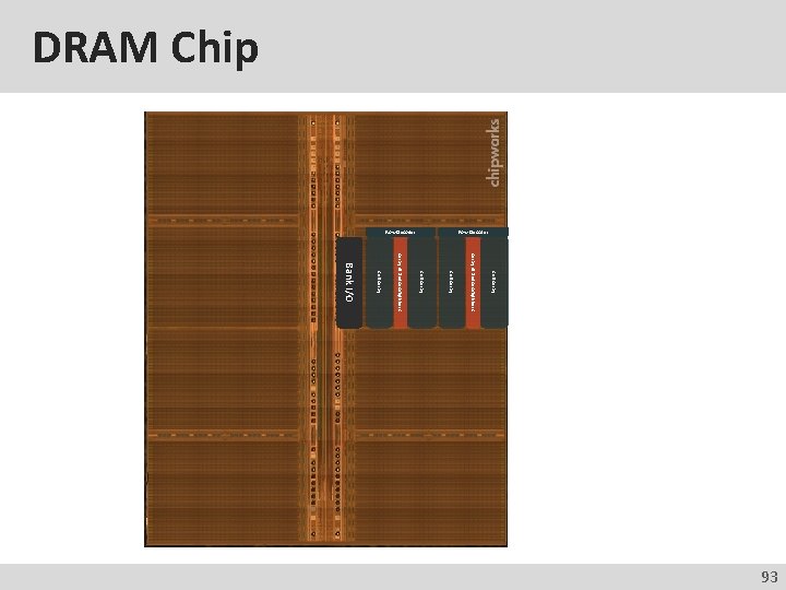
DRAM Chip Row Decoder Cell Array of Sense Amplifiers Cell Array Bank I/O 93

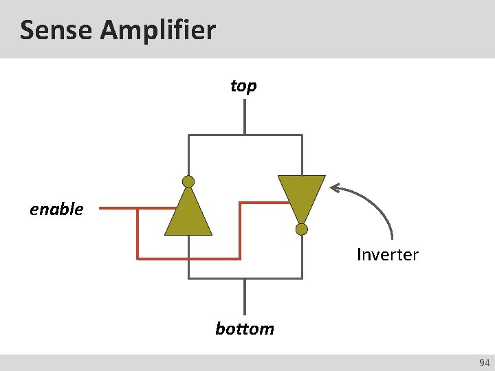
Sense Amplifier top enable Inverter bottom 94

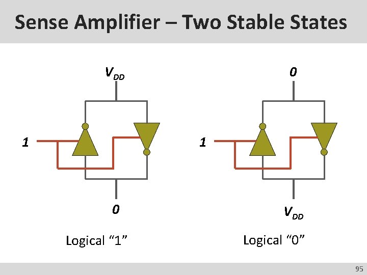
Sense Amplifier – Two Stable States VDD 1 0 Logical “ 1” VDD Logical “ 0” 95

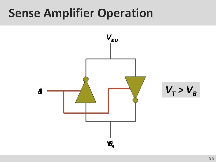
Sense Amplifier Operation VTDD VT > V B 0 1 V 0 B 96

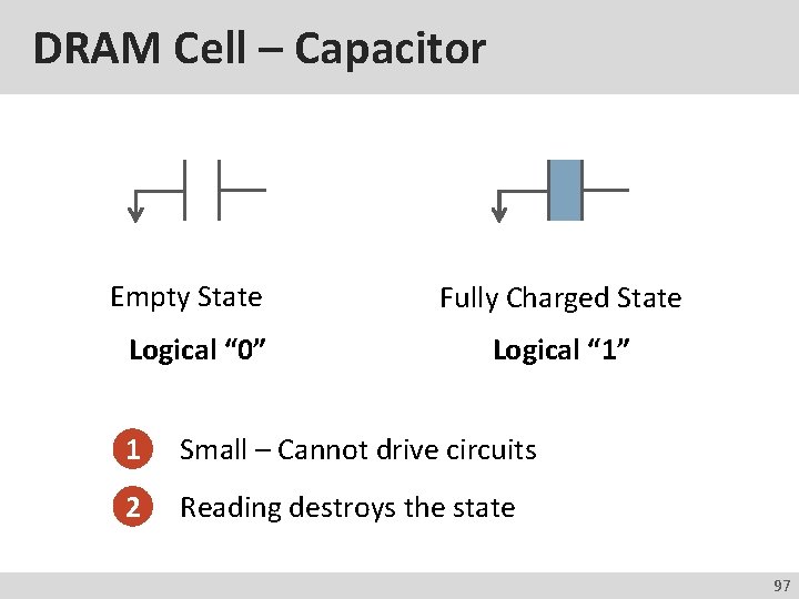
DRAM Cell – Capacitor Empty State Logical “ 0” Fully Charged State Logical “ 1” 1 Small – Cannot drive circuits 2 Reading destroys the state 97

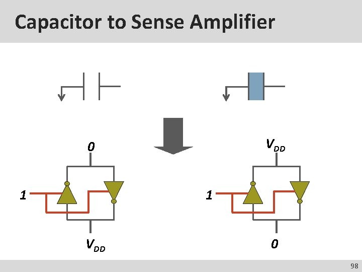
Capacitor to Sense Amplifier VDD 0 1 1 VDD 0 98

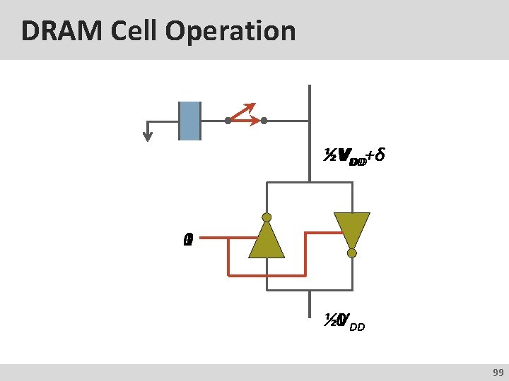
DRAM Cell Operation ½VVDD DD+δ 1 0 0 DD ½V 99

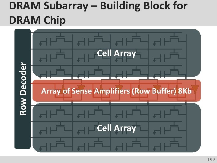
DRAM Subarray – Building Block for DRAM Chip Row Decoder Cell Array of Sense Amplifiers (Row Buffer) 8 Kb Cell Array 100

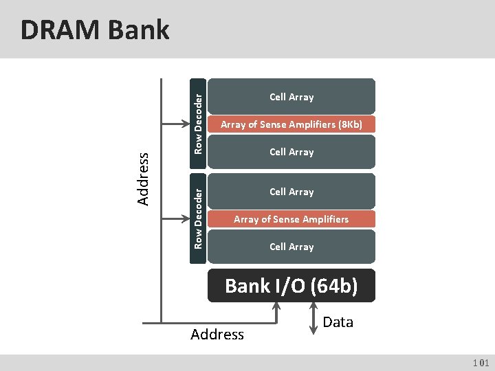
Row Decoder Address DRAM Bank Cell Array of Sense Amplifiers (8 Kb) Cell Array of Sense Amplifiers Cell Array Bank I/O (64 b) Address Data 101

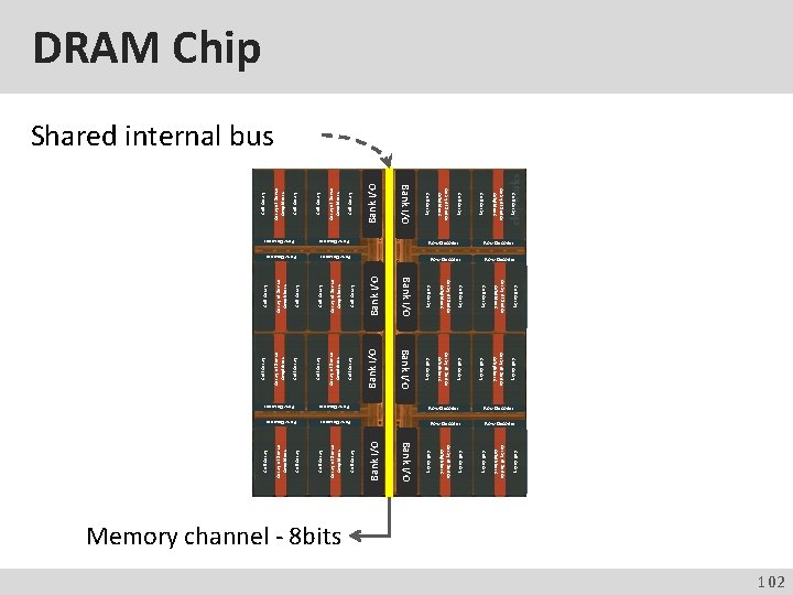
Cell Array of Sense Amplifiers Cell Array Bank I/O Cell Array Array of Sense Amplifiers Bank I/O Row Decoder Bank I/O Cell Array Array of Sense Amplifiers Cell Array Row Decoder Array of Sense Amplifiers Row Decoder Cell Array of Sense Amplifiers Cell Array Row Decoder Cell Array Cell Array of Sense Amplifiers Bank I/O Row Decoder Row Decoder Array of Sense Amplifiers Cell Array Array of Sense Amplifiers Cell Array Bank I/O Row Decoder Array of Sense Amplifiers DRAM Chip Shared internal bus Memory channel - 8 bits 102 Row Decoder

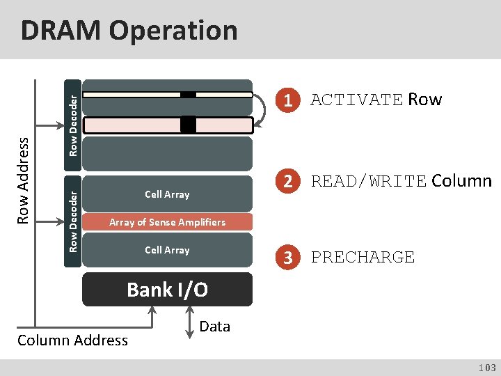
1 ACTIVATE Row Decoder Row Address DRAM Operation 2 READ/WRITE Column Cell Array of Sense Amplifiers Cell Array 3 PRECHARGE Bank I/O Column Address Data 103

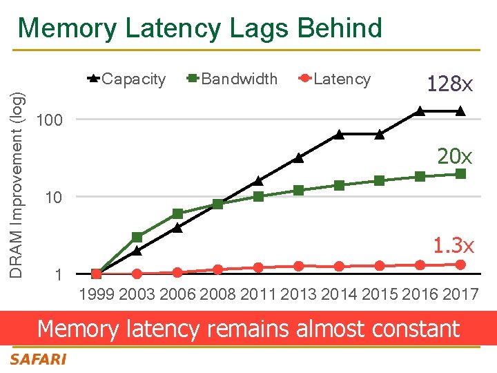
Memory Latency Lags Behind DRAM Improvement (log) Capacity Bandwidth Latency 128 x 100 20 x 10 1. 3 x 1 1999 2003 2006 2008 2011 2013 2014 2015 2016 2017 Memory latency remains almost constant

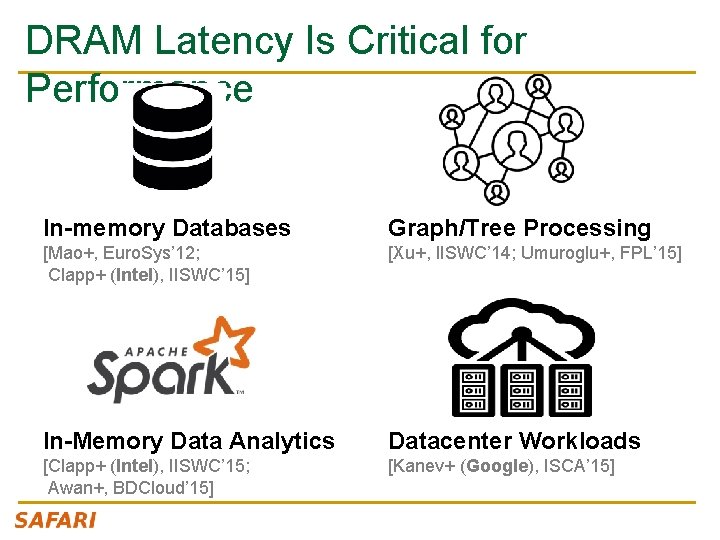
DRAM Latency Is Critical for Performance In-memory Databases Graph/Tree Processing [Mao+, Euro. Sys’ 12; Clapp+ (Intel), IISWC’ 15] [Xu+, IISWC’ 14; Umuroglu+, FPL’ 15] In-Memory Data Analytics Datacenter Workloads [Clapp+ (Intel), IISWC’ 15; Awan+, BDCloud’ 15] [Kanev+ (Google), ISCA’ 15]

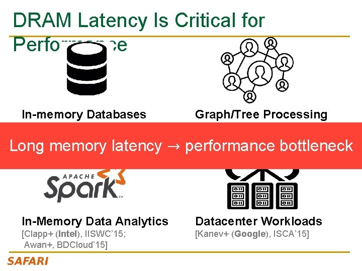
DRAM Latency Is Critical for Performance In-memory Databases Graph/Tree Processing [Mao+, Euro. Sys’ 12; Clapp+ (Intel), IISWC’ 15] [Xu+, IISWC’ 12; Umuroglu+, FPL’ 15] In-Memory Data Analytics Datacenter Workloads [Clapp+ (Intel), IISWC’ 15; Awan+, BDCloud’ 15] [Kanev+ (Google), ISCA’ 15] Long memory latency → performance bottleneck

What Causes the Long DRAM Latency?

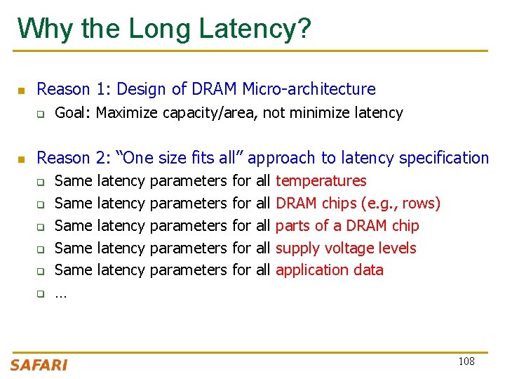
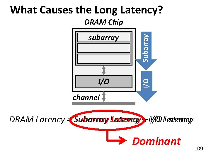
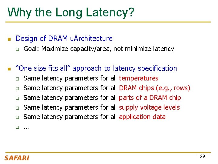
Why the Long Latency? n Reason 1: Design of DRAM Micro-architecture q n Goal: Maximize capacity/area, not minimize latency Reason 2: “One size fits all” approach to latency specification q q q Same latency parameters for all temperatures Same latency parameters for all DRAM chips (e. g. , rows) Same latency parameters for all parts of a DRAM chip Same latency parameters for all supply voltage levels Same latency parameters for all application data … 108

What Causes the Long Latency? I/O subarray cell array Subarray DRAM Chip channel DRAM Latency = Subarray Latency ++ I/O Latency Dominant 109

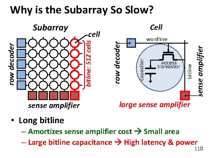
Why is the Subarray So Slow? sense amplifier access transistor bitline wordline capacitor row decoder sense amplifier Cell cell bitline: 512 cells Subarray large sense amplifier • Long bitline – Amortizes sense amplifier cost Small area – Large bitline capacitance High latency & power 110

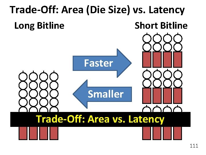
Trade-Off: Area (Die Size) vs. Latency Long Bitline Short Bitline Faster Smaller Trade-Off: Area vs. Latency 111

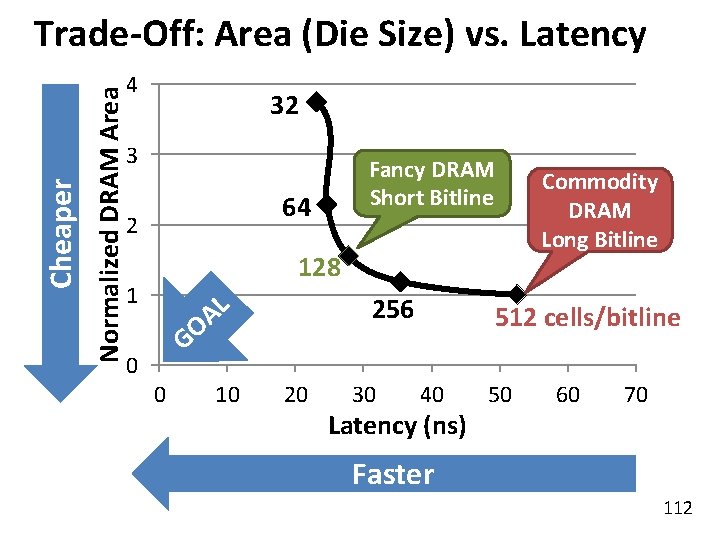
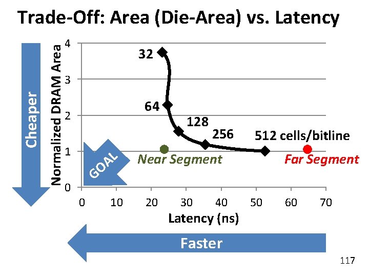
Normalized DRAM Area Cheaper Trade-Off: Area (Die Size) vs. Latency 4 32 3 Fancy DRAM Short Bitline 64 2 128 1 L A O 256 G 0 0 10 20 30 Commodity DRAM Long Bitline 512 cells/bitline 40 Latency (ns) 50 60 70 Faster 112

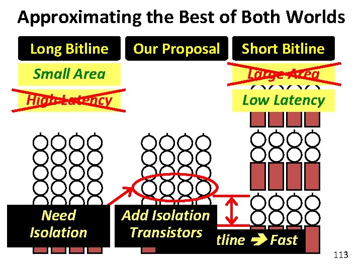
Approximating the Best of Both Worlds Long Bitline Our Proposal Short Bitline Small Area Large Area High Latency Low Latency Need Isolation Add Isolation Transistors Short Bitline Fast 113

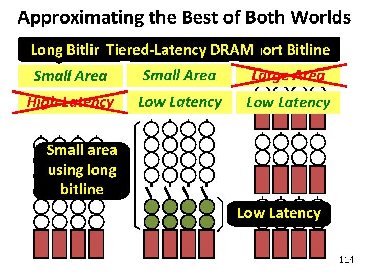
Approximating the Best of Both Worlds DRAMShort Long Our Proposal Long Bitline. Tiered-Latency Short Bitline Large Area Small Area High Latency Low Latency Small area using long bitline Low Latency 114

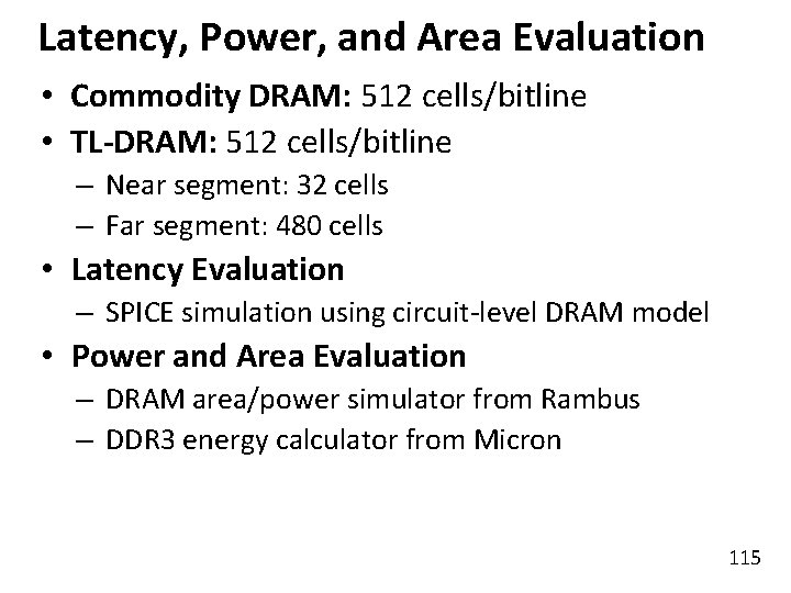
Latency, Power, and Area Evaluation • Commodity DRAM: 512 cells/bitline • TL-DRAM: 512 cells/bitline – Near segment: 32 cells – Far segment: 480 cells • Latency Evaluation – SPICE simulation using circuit-level DRAM model • Power and Area Evaluation – DRAM area/power simulator from Rambus – DDR 3 energy calculator from Micron 115
![Commodity DRAM vs TLDRAM HPCA 2013 DRAM Latency t RC DRAM Power Commodity DRAM vs. TL-DRAM [HPCA 2013] • DRAM Latency (t. RC) • DRAM Power](https://slidetodoc.com/presentation_image/543a808a2d6b1c173e05cf2e402ed7ec/image-116.jpg)
Commodity DRAM vs. TL-DRAM [HPCA 2013] • DRAM Latency (t. RC) • DRAM Power 100% +23% (52. 5 ns) 50% 0% Commodity DRAM – 56% Near +49% 150% Power Latency 150% Far TL-DRAM 100% 50% 0% Commodity DRAM – 51% Near Far TL-DRAM • DRAM Area Overhead ~3%: mainly due to the isolation transistors 116

Normalized DRAM Area Cheaper Trade-Off: Area (Die-Area) vs. Latency 4 32 3 64 2 1 L A O G 0 0 10 128 256 512 cells/bitline Near Segment 20 30 40 Latency (ns) Far Segment 50 60 70 Faster 117

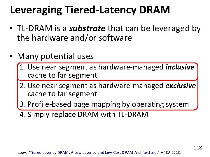
Leveraging Tiered-Latency DRAM • TL-DRAM is a substrate that can be leveraged by the hardware and/or software • Many potential uses 1. Use near segment as hardware-managed inclusive cache to far segment 2. Use near segment as hardware-managed exclusive cache to far segment 3. Profile-based page mapping by operating system 4. Simply replace DRAM with TL-DRAM Lee+, “Tiered-Latency DRAM: A Low Latency and Low Cost DRAM Architecture, ” HPCA 2013. 118

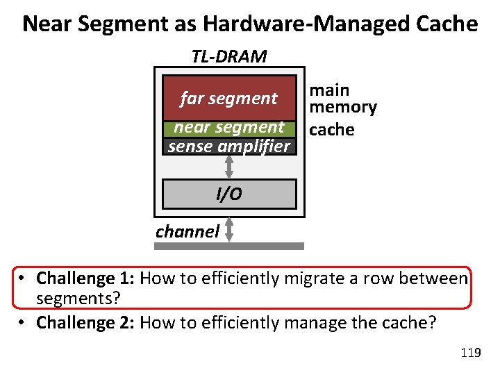
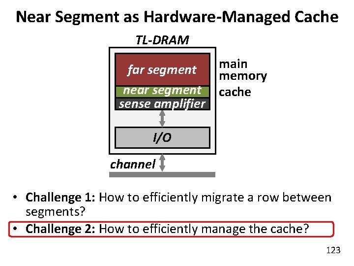
Near Segment as Hardware-Managed Cache TL-DRAM subarray main far segment memory near segment cache sense amplifier I/O channel • Challenge 1: How to efficiently migrate a row between segments? • Challenge 2: How to efficiently manage the cache? 119

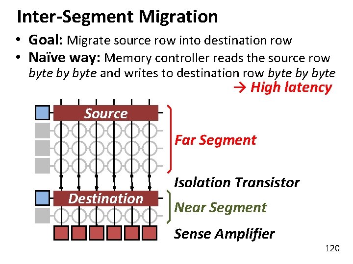
Inter-Segment Migration • Goal: Migrate source row into destination row • Naïve way: Memory controller reads the source row byte by byte and writes to destination row byte by byte → High latency Source Far Segment Destination Isolation Transistor Near Segment Sense Amplifier 120

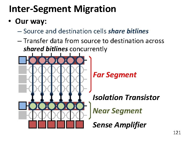
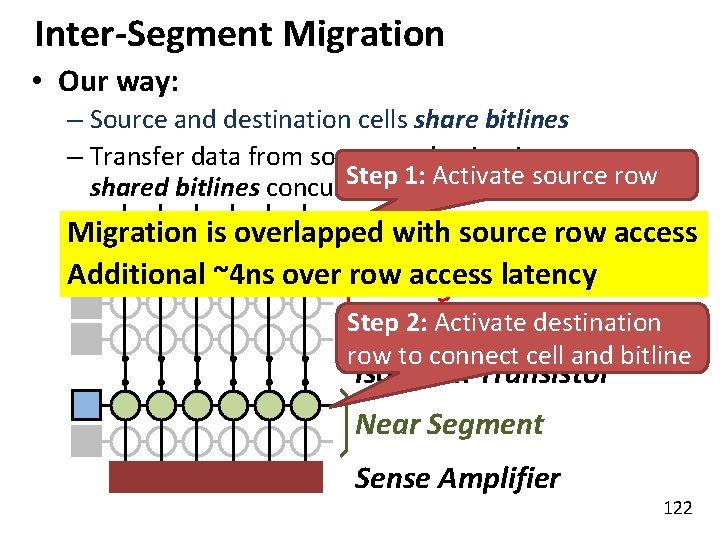
Inter-Segment Migration • Our way: – Source and destination cells share bitlines – Transfer data from source to destination across shared bitlines concurrently Source Far Segment Destination Isolation Transistor Near Segment Sense Amplifier 121

Inter-Segment Migration • Our way: – Source and destination cells share bitlines – Transfer data from source to destination across Step 1: Activate source row shared bitlines concurrently Migration is overlapped with source row access Additional ~4 ns over row access latency Far Segment Step 2: Activate destination row to connect cell and bitline Isolation Transistor Near Segment Sense Amplifier 122

Near Segment as Hardware-Managed Cache TL-DRAM subarray main far segment memory near segment cache sense amplifier I/O channel • Challenge 1: How to efficiently migrate a row between segments? • Challenge 2: How to efficiently manage the cache? 123

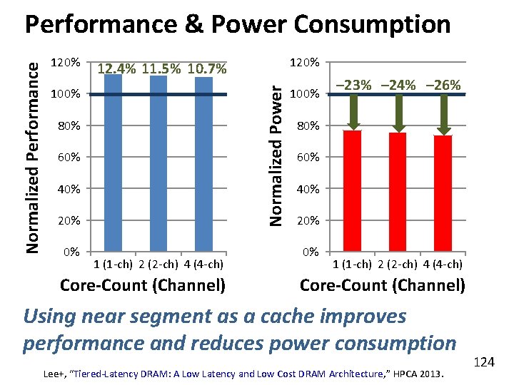
120% 100% 80% 60% 40% 20% 0% 12. 4% 11. 5% 10. 7% Normalized Power Normalized Performance & Power Consumption 1 (1 -ch) 2 (2 -ch) 4 (4 -ch) Core-Count (Channel) 100% – 23% – 24% – 26% 80% 60% 40% 20% 0% 1 (1 -ch) 2 (2 -ch) 4 (4 -ch) Core-Count (Channel) Using near segment as a cache improves performance and reduces power consumption Lee+, “Tiered-Latency DRAM: A Low Latency and Low Cost DRAM Architecture, ” HPCA 2013. 124

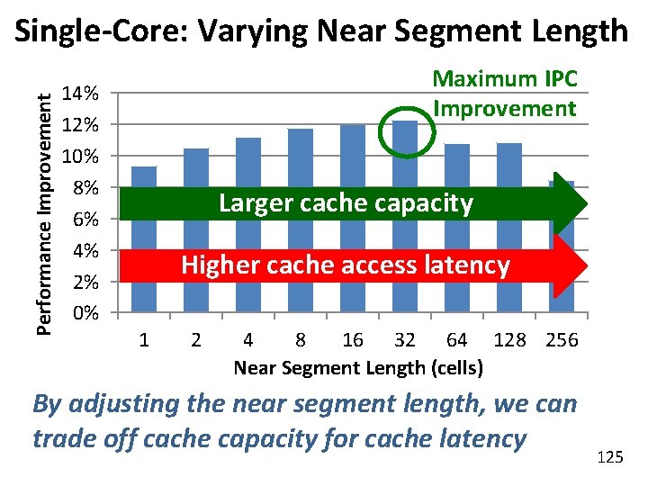
Performance Improvement Single-Core: Varying Near Segment Length Maximum IPC Improvement 14% 12% 10% 8% 6% 4% 2% 0% Larger cache capacity Higher cache access latency 1 2 4 8 16 32 64 128 256 Near Segment Length (cells) By adjusting the near segment length, we can trade off cache capacity for cache latency 125

More on TL-DRAM n Donghyuk Lee, Yoongu Kim, Vivek Seshadri, Jamie Liu, Lavanya Subramanian, and Onur Mutlu, "Tiered-Latency DRAM: A Low Latency and Low Cost DRAM Architecture" Proceedings of the 19 th International Symposium on High. Performance Computer Architecture (HPCA), Shenzhen, China, February 2013. Slides (pptx) 126

We did not cover the following slides in lecture. These are for your preparation for the next lecture.

Computer Architecture Lecture 5: DRAM Operation, Memory Control & Memory Latency Prof. Onur Mutlu ETH Zürich Fall 2017 4 October 2017

Why the Long Latency? n Design of DRAM u. Architecture q n Goal: Maximize capacity/area, not minimize latency “One size fits all” approach to latency specification q q q Same latency parameters for all temperatures Same latency parameters for all DRAM chips (e. g. , rows) Same latency parameters for all parts of a DRAM chip Same latency parameters for all supply voltage levels Same latency parameters for all application data … 129

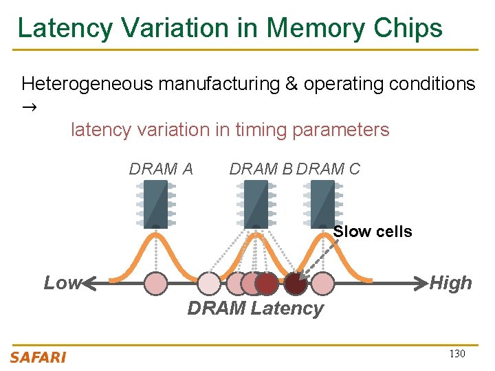
Latency Variation in Memory Chips Heterogeneous manufacturing & operating conditions → latency variation in timing parameters DRAM A DRAM B DRAM C Slow cells Low High DRAM Latency 130

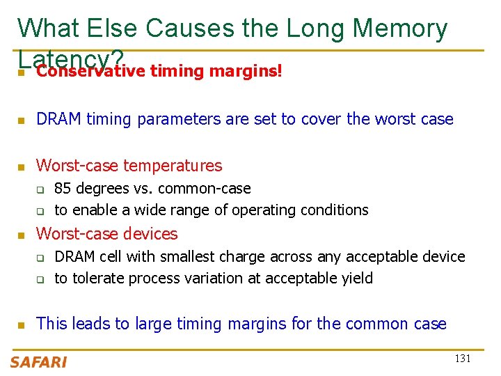
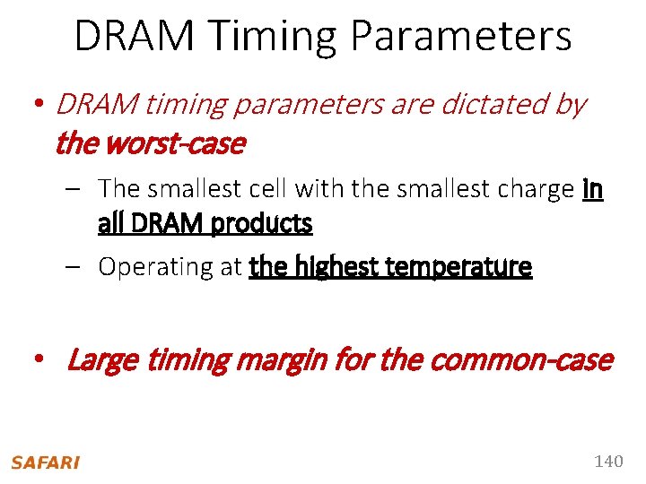
What Else Causes the Long Memory Latency? n Conservative timing margins! n DRAM timing parameters are set to cover the worst case n Worst-case temperatures q q n Worst-case devices q q n 85 degrees vs. common-case to enable a wide range of operating conditions DRAM cell with smallest charge across any acceptable device to tolerate process variation at acceptable yield This leads to large timing margins for the common case 131

Understanding and Exploiting Variation in DRAM Latency

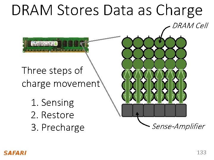
DRAM Stores Data as Charge DRAM Cell Three steps of charge movement 1. Sensing 2. Restore 3. Precharge Sense-Amplifier 133

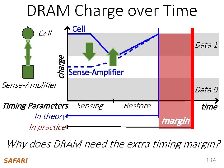
DRAM Charge over Time Cell charge Data 1 Sense-Amplifier Timing Parameters Sensing In theory In practice Data 0 Restore time margin Why does DRAM need the extra timing margin? 134

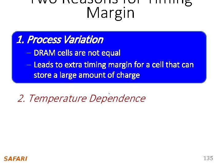
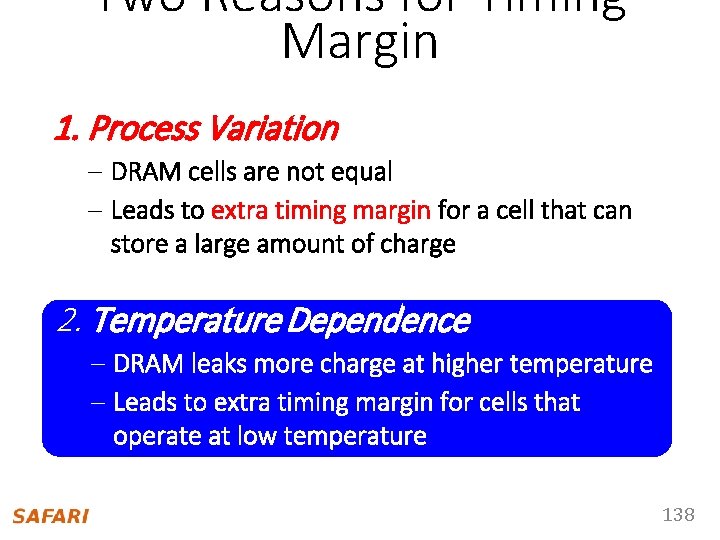
Two Reasons for Timing Margin 1. Process Variation – DRAM cells are not equal – Leads to extra timing margin for acellthatcan store asmall largeamountofofcharge 2. Temperature Dependence ` – DRAM leaks more charge at higher temperature – Leads to extra timing margin when operating at low temperature 135

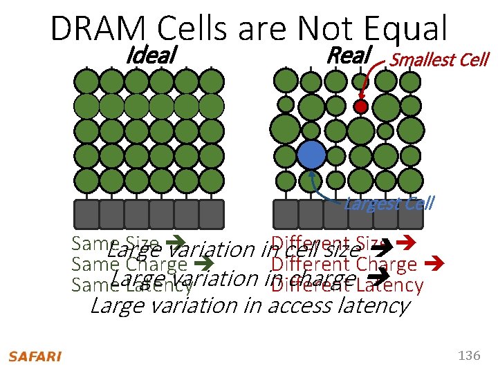
DRAM Cells are Not Equal Ideal Real Smallest Cell Largest Cell Same Size Large variation in. Different cell size. Size Same Charge Different Charge Large variation in. Different charge Latency Same Latency Large variation in access latency 136

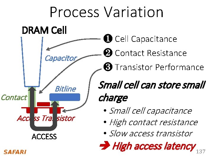
Process Variation DRAM Cell Contact ❶ Cell Capacitance Capacitor ❷ Contact Resistance ❸ Transistor Performance Bitline Small cell can store small charge Access Transistor ACCESS • Small cell capacitance • High contact resistance • Slow access transistor High access latency 137

Two Reasons for Timing Margin 1. Process Variation – DRAM cells are not equal – Leads to extra timing margin for a cell that can store a large amount of charge 2. Temperature Dependence ` – DRAM leaks more charge at higher temperature – Leads to extra timing margin for cells that operate at low temperature the high temperature 138

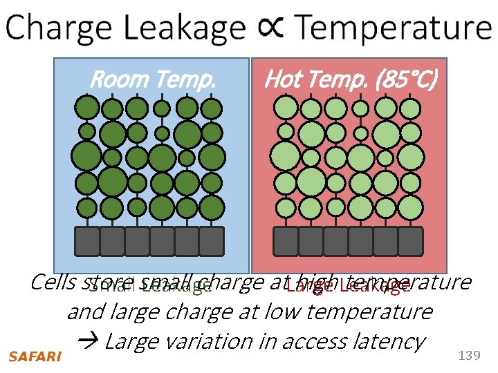
Room Temp. Hot Temp. (85°C) Cells store charge at. Large high Leakage temperature Small small Leakage and large charge at low temperature Large variation in access latency 139

DRAM Timing Parameters • DRAM timing parameters are dictated by the worst-case – The smallest cell with the smallest charge in all DRAM products – Operating at the highest temperature • Large timing margin for the common-case 140
![AdaptiveLatency DRAM HPCA 2015 n Idea Optimize DRAM timing for the common case q Adaptive-Latency DRAM [HPCA 2015] n Idea: Optimize DRAM timing for the common case q](https://slidetodoc.com/presentation_image/543a808a2d6b1c173e05cf2e402ed7ec/image-141.jpg)
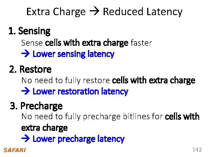
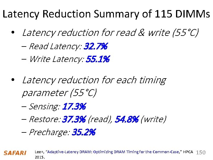
Adaptive-Latency DRAM [HPCA 2015] n Idea: Optimize DRAM timing for the common case q q n Current temperature Current DRAM module Why would this reduce latency? q A DRAM cell can store much more charge in the common case (low temperature, strong cell) than in the worst case More charge in a DRAM cell Faster sensing, charge restoration, precharging Faster access (read, write, refresh, …) q Lee+, “Adaptive-Latency DRAM: Optimizing DRAM Timing for the Common-Case, ” 141 HPCA 2015.

Extra Charge Reduced Latency 1. Sensing Sense cells with extra charge faster Lower sensing latency 2. Restore No need to fully restore cells with extra charge Lower restoration latency 3. Precharge No need to fully precharge bitlines for cells with extra charge Lower precharge latency 142

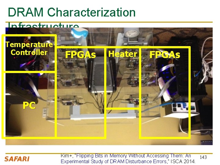
DRAM Characterization Infrastructure Temperature Controller FPGAs Heater FPGAs PC Kim+, “Flipping Bits in Memory Without Accessing Them: An 143 Experimental Study of DRAM Disturbance Errors, ” ISCA 2014.

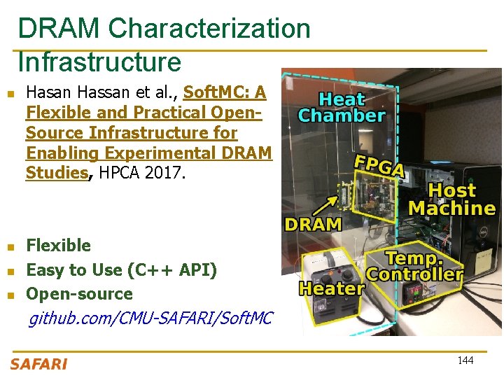
DRAM Characterization Infrastructure n n Hasan Hassan et al. , Soft. MC: A Flexible and Practical Open. Source Infrastructure for Enabling Experimental DRAM Studies, HPCA 2017. Flexible Easy to Use (C++ API) Open-source github. com/CMU-SAFARI/Soft. MC 144

Soft. MC: Open Source DRAM Infrastructure n https: //github. com/CMU-SAFARI/Soft. MC 145

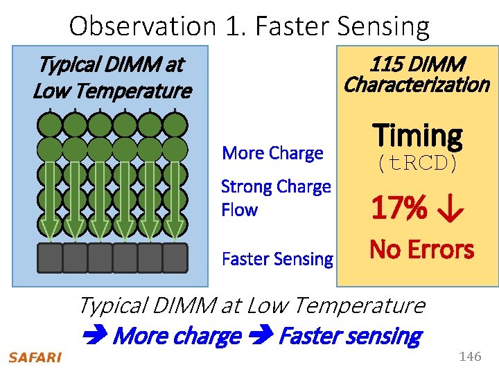
Observation 1. Faster Sensing 115 DIMM Characterization Typical DIMM at Low Temperature More Charge Timing (t. RCD) Strong Charge Flow 17% ↓ Faster Sensing No Errors Typical DIMM at Low Temperature More charge Faster sensing 146

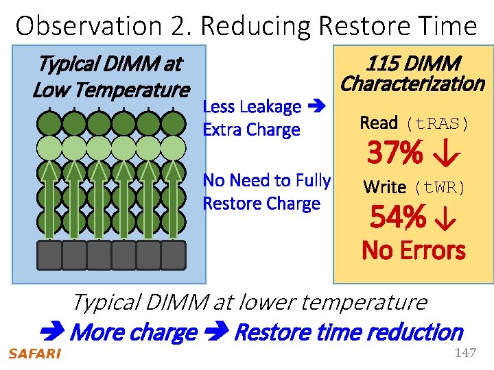
Observation 2. Reducing Restore Time Typical DIMM at Low Temperature Less Leakage Extra Charge No Need to Fully Restore Charge 115 DIMM Characterization Read (t. RAS) 37% ↓ Write (t. WR) 54% ↓ No Errors Typical DIMM at lower temperature More charge Restore time reduction 147

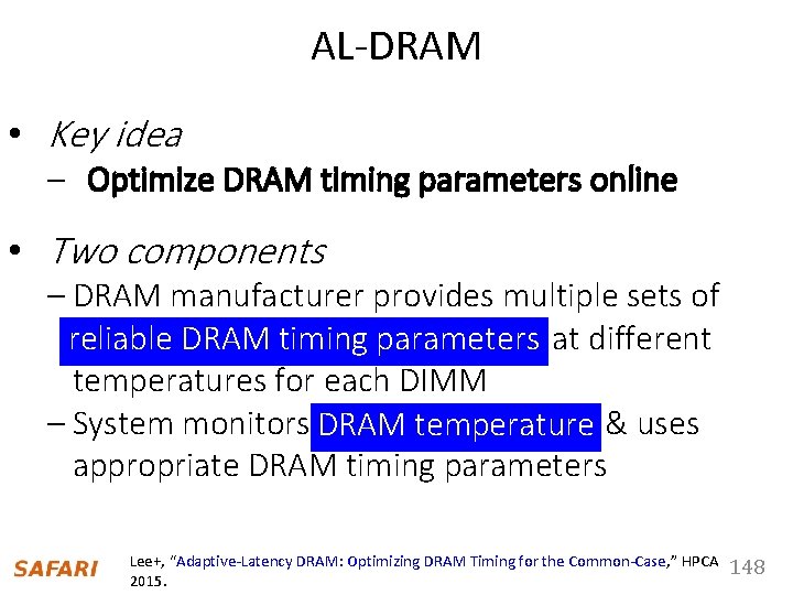
AL-DRAM • Key idea – Optimize DRAM timing parameters online • Two components – DRAM manufacturer provides multiple sets of reliable DRAM timing parameters at different reliable temperatures for each DIMM – System monitors DRAM temperature & uses appropriate DRAM timing parameters Lee+, “Adaptive-Latency DRAM: Optimizing DRAM Timing for the Common-Case, ” HPCA 2015. 148

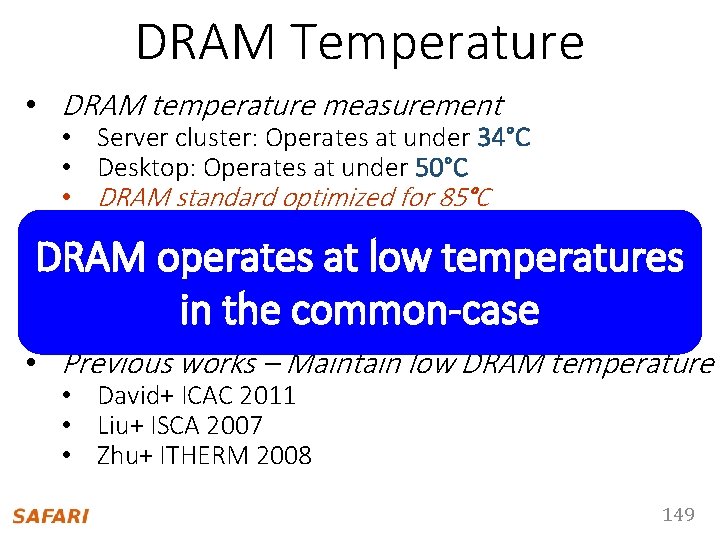
DRAM Temperature • DRAM temperature measurement • Server cluster: Operates at under 34°C • Desktop: Operates at under 50°C • DRAM standard optimized for 85°C • DRAM Previousoperates works – DRAM temperature is low at low temperatures • El-Sayed+ SIGMETRICS 2012 in 2007 the common-case • Liu+ ISCA • Previous works – Maintain low DRAM temperature • David+ ICAC 2011 • Liu+ ISCA 2007 • Zhu+ ITHERM 2008 149

Latency Reduction Summary of 115 DIMMs • Latency reduction for read & write (55°C) – Read Latency: 32. 7% – Write Latency: 55. 1% • Latency reduction for each timing parameter (55°C) – Sensing: 17. 3% – Restore: 37. 3% (read), 54. 8% (write) – Precharge: 35. 2% Lee+, “Adaptive-Latency DRAM: Optimizing DRAM Timing for the Common-Case, ” HPCA 2015. 150

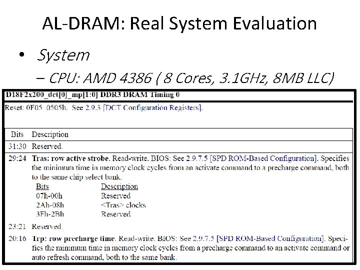
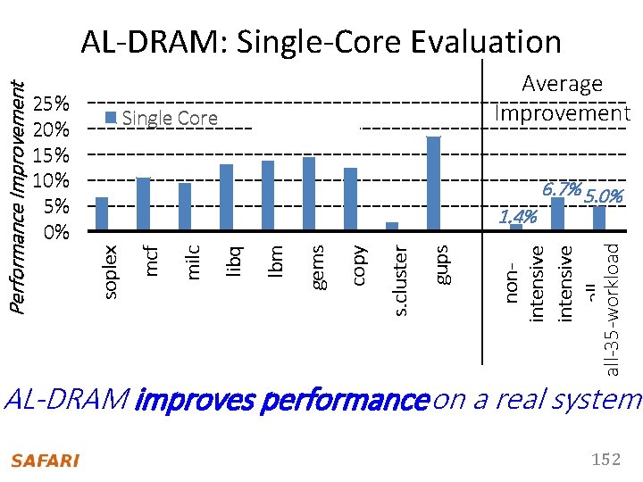
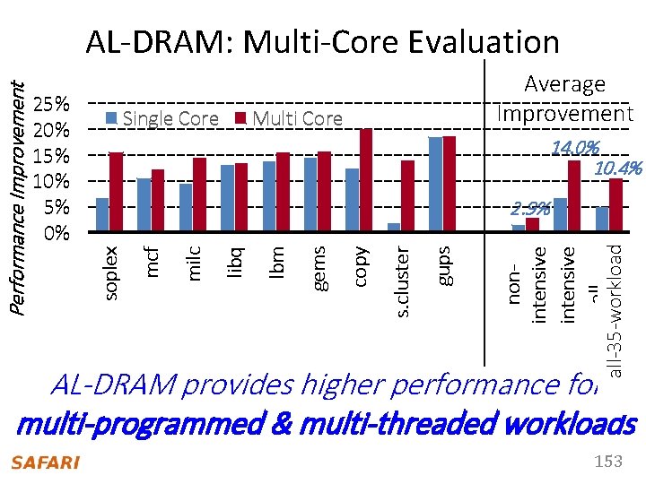
AL-DRAM: Real System Evaluation • System – CPU: AMD 4386 ( 8 Cores, 3. 1 GHz, 8 MB LLC) – DRAM: 4 GByte DDR 3 -1600 (800 Mhz Clock) – OS: Linux – Storage: 128 GByte SSD • Workload – 35 applications from SPEC, STREAM, Parsec, Memcached, Apache, GUPS 151

Single Core Average Improvement Multi Core 6. 7% 5. 0% nonintensive allall-35 -workloads gups s. cluster copy gems lbm libq milc 1. 4% mcf 25% 20% 15% 10% 5% 0% soplex Performance Improvement AL-DRAM: Single-Core Evaluation AL-DRAM improves performance on a real system 152

Single Core Average Improvement Multi Core 14. 0% 10. 4% nonintensive allall-35 -workloads gups s. cluster copy gems lbm libq milc 2. 9% mcf 25% 20% 15% 10% 5% 0% soplex Performance Improvement AL-DRAM: Multi-Core Evaluation AL-DRAM provides higher performance for multi-programmed & multi-threaded workloads 153

Reducing Latency Also Reduces Energy n AL-DRAM reduces DRAM power consumption by 5. 8% n Major reason: reduction in row activation time 154

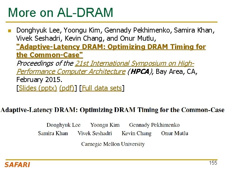
More on AL-DRAM n Donghyuk Lee, Yoongu Kim, Gennady Pekhimenko, Samira Khan, Vivek Seshadri, Kevin Chang, and Onur Mutlu, "Adaptive-Latency DRAM: Optimizing DRAM Timing for the Common-Case" Proceedings of the 21 st International Symposium on High. Performance Computer Architecture (HPCA), Bay Area, CA, February 2015. [Slides (pptx) (pdf)] [Full data sets] 155

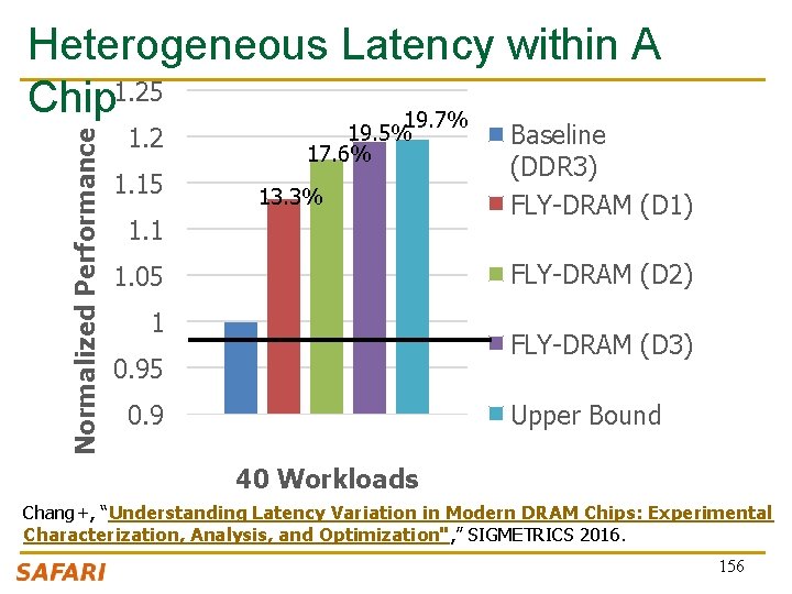
Normalized Performance Heterogeneous Latency within A Chip 1. 25 19. 7% 1. 2 1. 15 19. 5% 17. 6% 13. 3% 1. 1 Baseline (DDR 3) FLY-DRAM (D 1) FLY-DRAM (D 2) 1. 05 1 FLY-DRAM (D 3) 0. 95 Upper Bound 0. 9 40 Workloads Chang+, “Understanding Latency Variation in Modern DRAM Chips: Experimental Characterization, Analysis, and Optimization", ” SIGMETRICS 2016. 156

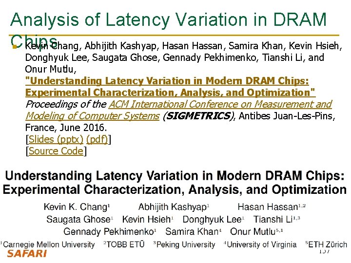
Analysis of Latency Variation in DRAM Chips Kevin Chang, Abhijith Kashyap, Hasan Hassan, Samira Khan, Kevin Hsieh, n Donghyuk Lee, Saugata Ghose, Gennady Pekhimenko, Tianshi Li, and Onur Mutlu, "Understanding Latency Variation in Modern DRAM Chips: Experimental Characterization, Analysis, and Optimization" Proceedings of the ACM International Conference on Measurement and Modeling of Computer Systems (SIGMETRICS), Antibes Juan-Les-Pins, France, June 2016. [Slides (pptx) (pdf)] [Source Code] 157

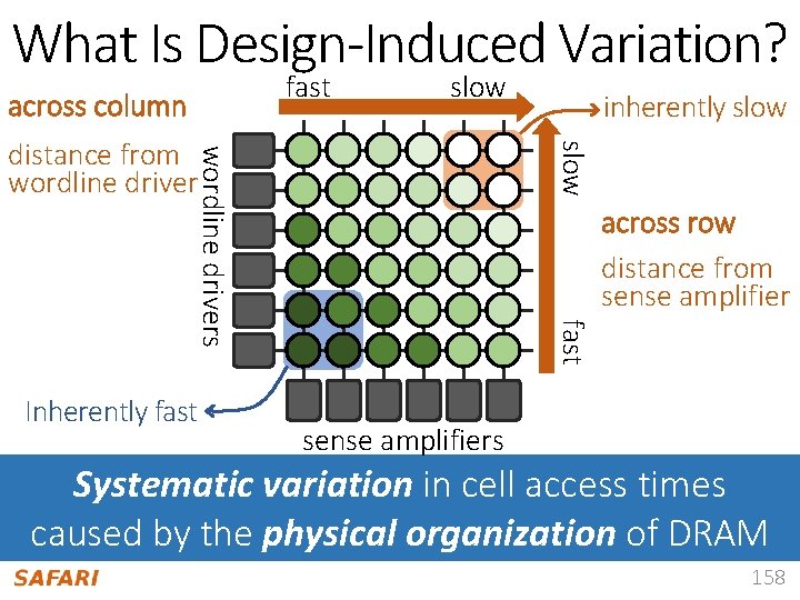
What Is Design-Induced Variation? fast across column slow wordline drivers slow distance from wordline driver across row distance from sense amplifier fast Inherently fast inherently slow sense amplifiers Systematic variation in cell access times caused by the physical organization of DRAM 158

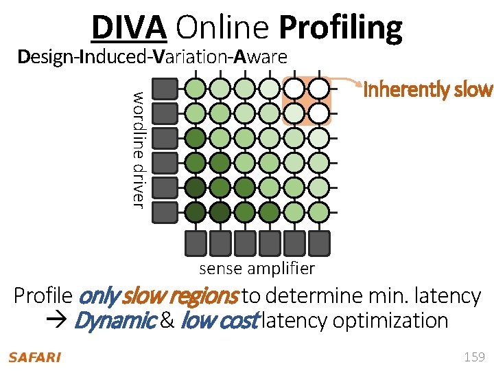
DIVA Online Profiling Design-Induced-Variation-Aware wordline driver inherently slow sense amplifier Profile only slow regions to determine min. latency Dynamic & low cost latency optimization 159

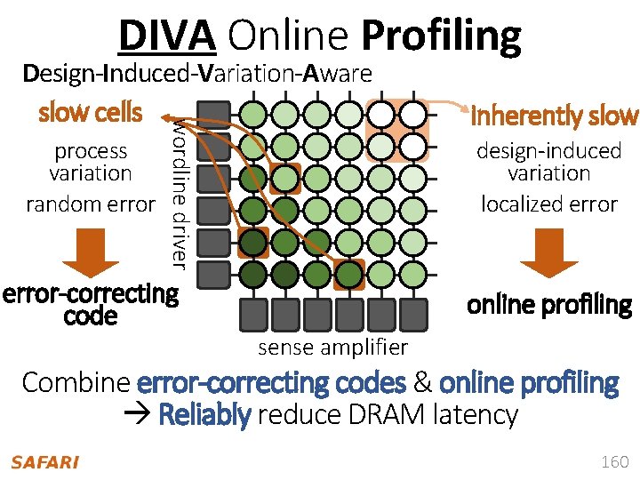
DIVA Online Profiling inherently slow process variation random error design-induced variation localized error wordline driver Design-Induced-Variation-Aware slow cells error-correcting code online profiling sense amplifier Combine error-correcting codes & online profiling Reliably reduce DRAM latency 160

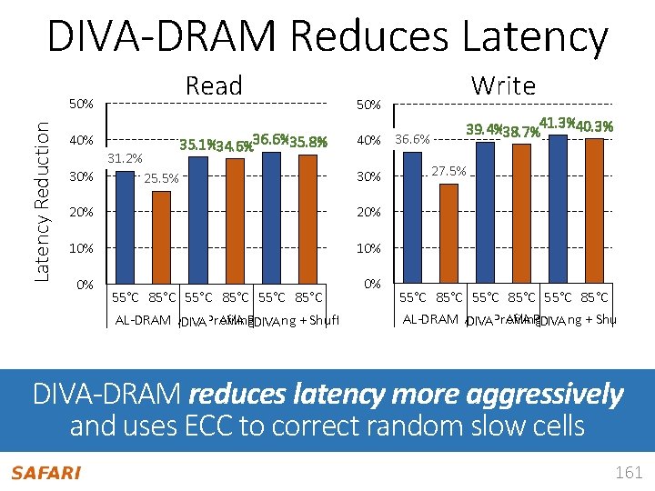
DIVA-DRAM Reduces Latency Read Latency Reduction 50% 40% 31. 2% 30% 35. 1%34. 6%36. 6%35. 8% 25. 5% Write 50% 40% 36. 6% 30% 20% 10% 0% 0% 55°C 85°C AL-DRAM AVA Profiling DIVA + Shuffling 39. 4%38. 7%41. 3%40. 3% 27. 5% 55°C 85°C AL-DRAM AVA Profiling DIVA + Shuffling DIVA-DRAM reduces latency more aggressively and uses ECC to correct random slow cells 161

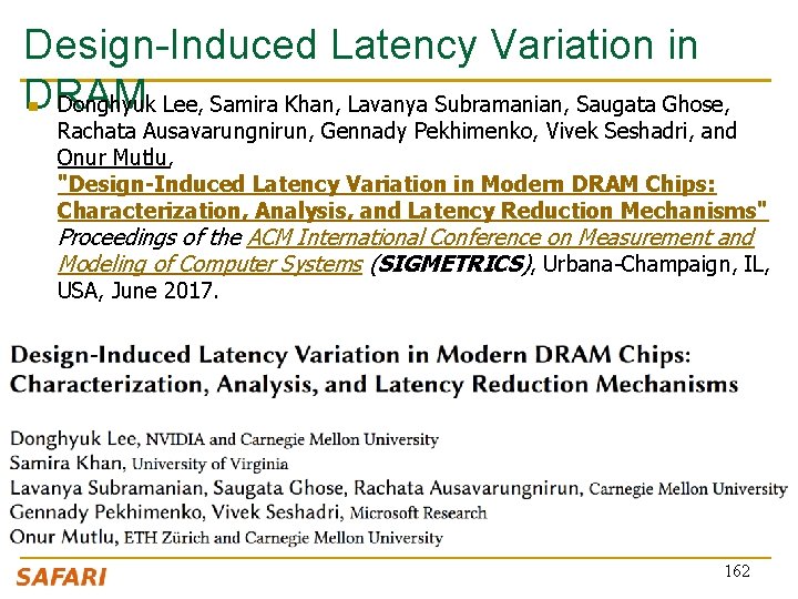
Design-Induced Latency Variation in DRAM Donghyuk Lee, Samira Khan, Lavanya Subramanian, Saugata Ghose, n Rachata Ausavarungnirun, Gennady Pekhimenko, Vivek Seshadri, and Onur Mutlu, "Design-Induced Latency Variation in Modern DRAM Chips: Characterization, Analysis, and Latency Reduction Mechanisms" Proceedings of the ACM International Conference on Measurement and Modeling of Computer Systems (SIGMETRICS), Urbana-Champaign, IL, USA, June 2017. 162

Voltron: Exploiting the Voltage-Latency. Reliability Relationship 163

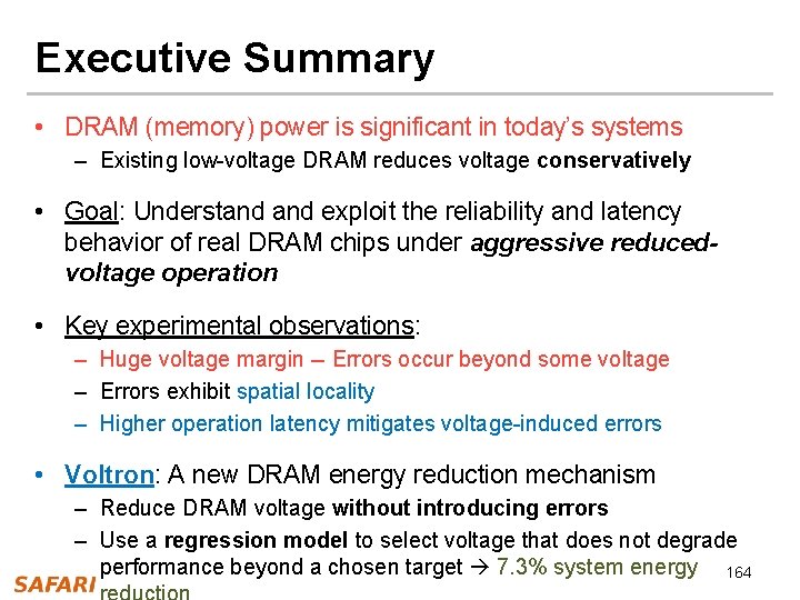
Executive Summary • DRAM (memory) power is significant in today’s systems – Existing low-voltage DRAM reduces voltage conservatively • Goal: Understand exploit the reliability and latency behavior of real DRAM chips under aggressive reducedvoltage operation • Key experimental observations: – Huge voltage margin -- Errors occur beyond some voltage – Errors exhibit spatial locality – Higher operation latency mitigates voltage-induced errors • Voltron: A new DRAM energy reduction mechanism – Reduce DRAM voltage without introducing errors – Use a regression model to select voltage that does not degrade performance beyond a chosen target 7. 3% system energy 164

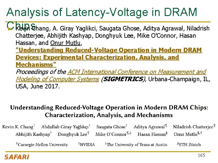
Analysis of Latency-Voltage in DRAM Chips Kevin Chang, A. Giray Yaglikci, Saugata Ghose, Aditya Agrawal, Niladrish n Chatterjee, Abhijith Kashyap, Donghyuk Lee, Mike O'Connor, Hasan Hassan, and Onur Mutlu, "Understanding Reduced-Voltage Operation in Modern DRAM Devices: Experimental Characterization, Analysis, and Mechanisms" Proceedings of the ACM International Conference on Measurement and Modeling of Computer Systems (SIGMETRICS), Urbana-Champaign, IL, USA, June 2017. 165

And, What If … n … we can sacrifice reliability of some data to access it with even lower latency? 166

Challenge and Opportunity for Future Fundamentally Low Latency Computing Architectures 167

Computer Architecture Lecture 5: DRAM Operation, Memory Control & Memory Latency Prof. Onur Mutlu ETH Zürich Fall 2017 4 October 2017