Computer Architecture I Digital Design Dr Robert D
Computer Architecture I: Digital Design Dr. Robert D. Kent CPU Registers Register Transfer and Microoperations
Review • We have introduced registers previously. • Registers are constructed using flip-flops and combinational circuits that enable one to: – Refresh volatile data – Load (Store) data – Clear storages (change all bits to 0) – Increment (and decrement) storages binarily – Complement storages – Select individual storage bits
Considering the next problem in design • When designing complex computer systems it is important to understand that we start from very small components for which the operational characteristics are extremely well defined. • We then applied Bottom-Up Hierarchical design to identify commonly used networks (ie. circuits) of smaller components, from SSI to MSI. At this stage the descriptive language (and symbols) changes. – SSI: + as OR transforms to MSI: + as ADD • Now as we consider MSI to LSI, and also MSI-to-MSI networks, such as the CPU, our language must again change to fit the nature of design.
Goals • The Mano model of the CPU Registers – Bus network • Register and Memory Transfer – A language for describing hardware function – A language for denoting implementation – A language that bridges LSI/MSI • Microoperations: Application examples – Arithmetic – Logic – Shift
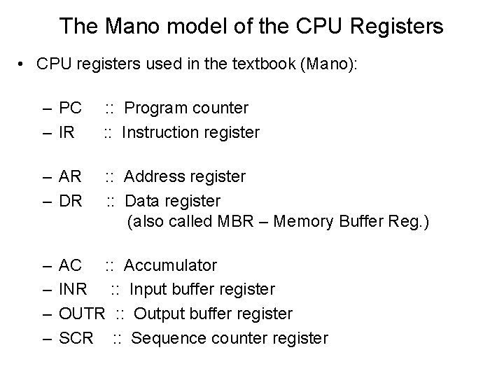
The Mano model of the CPU Registers • CPU registers used in the textbook (Mano): – PC – IR : : Program counter : : Instruction register – AR – DR : : Address register : : Data register (also called MBR – Memory Buffer Reg. ) – – AC : : Accumulator INR : : Input buffer register OUTR : : Output buffer register SCR : : Sequence counter register
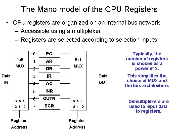
The Mano model of the CPU Registers • CPU registers are organized on an internal bus network – Accessible using a multiplexer – Registers are selected according to selection inputs 0 PC 1 AR 2 DR Data 3 IR Data IN 4 AC OUT 5 INR S S S 6 OUTR 2 1 0 7 SCR 1 x 8 MUX Typically, the number of registers is chosen as a power of 2. 8 x 1 MUX S S S 2 1 0 Register Address This simplifies the choice of MUX and the bus architecture. Demultiplexers are used to input data to registers.
Reminder! • CPU register operations should be among the fastest of hardware operations – All instructions are executed in CPU – Few registers implies more complex circuits may be employed to control data processing and workflow – We need a language that allows us to describe what we want to happen (operationally) in a circuit, while achieving an actual working hardware system to accomplish our requirements • We must also understand the complexities or behaviours of the circuits, such as performance based on numbers of logic stages, degrees of parallel versus serial capacity, response and other factors
Register Transfer • First, review what we have learned so far about registers – We combined the basic building blocks of bit storage units (ie. flip-flops) to form storage units of multiple bits called registers – We combined registers with more complicated circuitry to perform various operations • Some serial operations • Some parallel operations – We combined several operations together into even more complicated circuits • The choice of operation is determined by Selector inputs using either Multi-Input Control, or Multiplexer Selection.
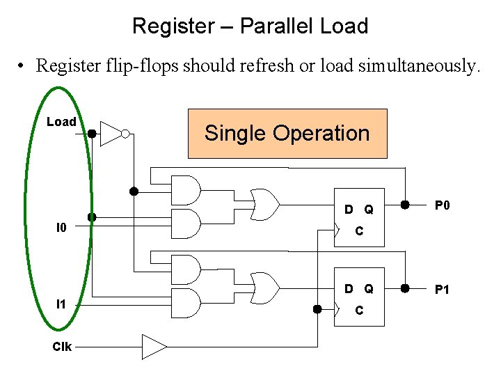
Register – Parallel Load • Register flip-flops should refresh or load simultaneously. Load Single Operation D Q I 0 C D Q I 1 Clk P 0 C P 1
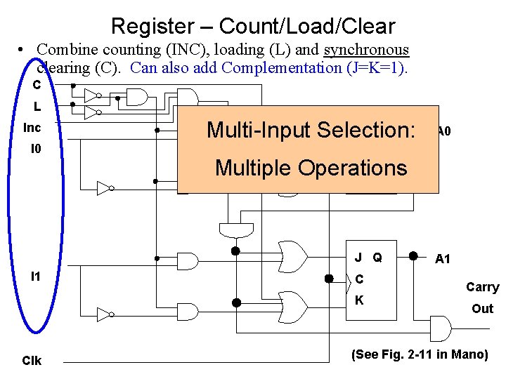
Register – Count/Load/Clear • Combine counting (INC), loading (L) and synchronous clearing (C). Can also add Complementation (J=K=1). C L Inc I 0 J Q Multi-Input Selection: C Multiple Operations K J Q I 1 C K Clk A 0 A 1 Carry Out (See Fig. 2 -11 in Mano)
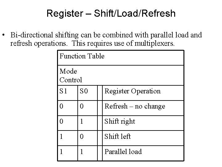
Register – Shift/Load/Refresh • Bi-directional shifting can be combined with parallel load and refresh operations. This requires use of multiplexers. Function Table Mode Control S 1 S 0 Register Operation 0 0 Refresh – no change 0 1 Shift right 1 0 Shift left 1 1 Parallel load
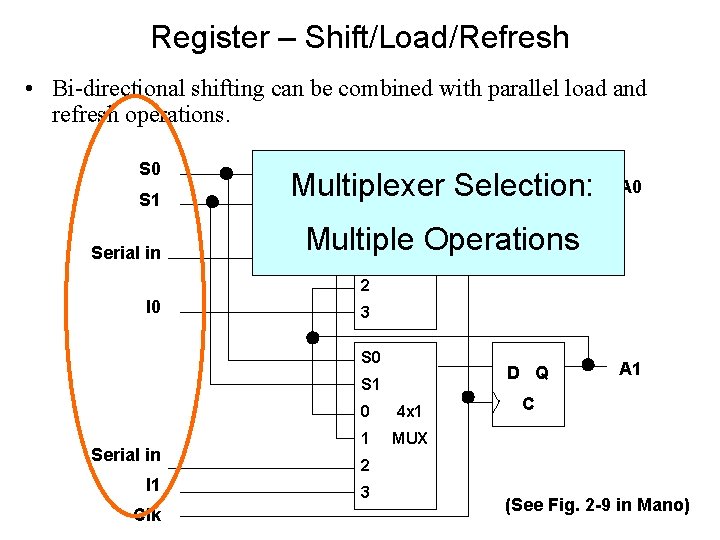
Register – Shift/Load/Refresh • Bi-directional shifting can be combined with parallel load and refresh operations. S 0 S 1 Multiplexer Selection: D Q S 1 S 0 C Multiple Operations 1 MUX 0 Serial in A 0 4 x 1 2 I 0 3 S 0 D Q S 1 Serial in I 1 Clk 0 4 x 1 1 MUX A 1 C 2 3 (See Fig. 2 -9 in Mano)
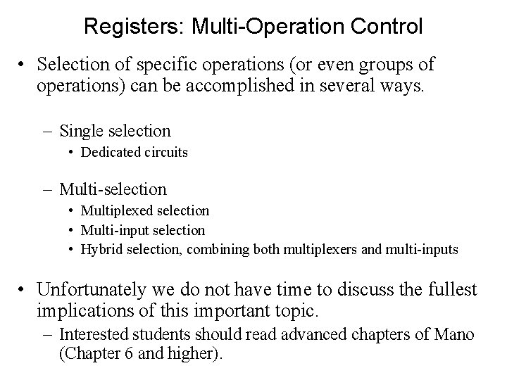
Registers: Multi-Operation Control • Selection of specific operations (or even groups of operations) can be accomplished in several ways. – Single selection • Dedicated circuits – Multi-selection • Multiplexed selection • Multi-input selection • Hybrid selection, combining both multiplexers and multi-inputs • Unfortunately we do not have time to discuss the fullest implications of this important topic. – Interested students should read advanced chapters of Mano (Chapter 6 and higher).
Register Transfer • The internal hardware organization of a digital computer is best defined by specifying: – The set of registers it contains and their function – The sequence of microoperations performed on the binary data stored in the registers – The control that initiates the sequence of microoperations
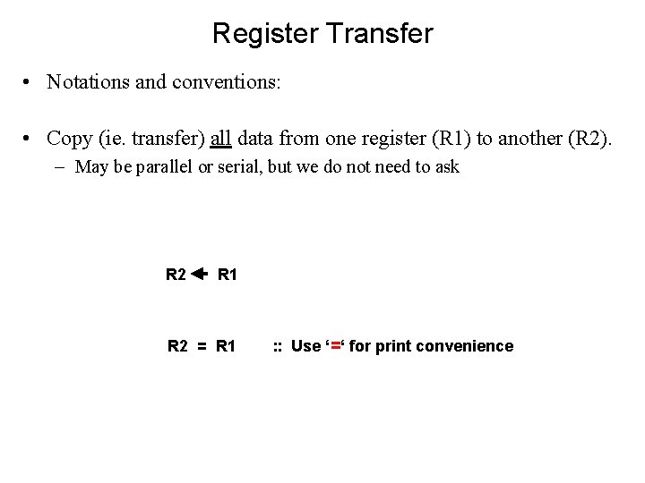
Register Transfer • Notations and conventions: • Copy (ie. transfer) all data from one register (R 1) to another (R 2). – May be parallel or serial, but we do not need to ask R 2 R 1 R 2 = R 1 : : Use ‘=‘ for print convenience
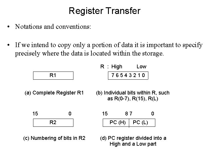
Register Transfer • Notations and conventions: • If we intend to copy only a portion of data it is important to specify precisely where the data is located within the storage. R : High R 1 76543210 (a) Complete Register R 1 15 Low 0 R 2 (c) Numbering of bits in R 2 (b) Individual bits within R, such as R(0 -7), R(15), R(L) 15 87 PC (H) 0 PC (L) (d) PC register divided into a High and a Low part
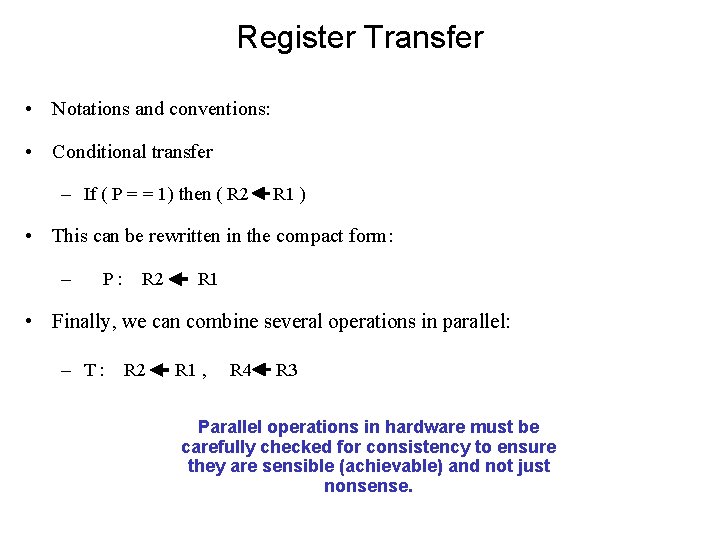
Register Transfer • Notations and conventions: • Conditional transfer – If ( P = = 1) then ( R 2 R 1 ) • This can be rewritten in the compact form: – P: R 2 R 1 • Finally, we can combine several operations in parallel: – T : R 2 R 1 , R 4 R 3 Parallel operations in hardware must be carefully checked for consistency to ensure they are sensible (achievable) and not just nonsense.
Memory • RAM storages are typically constructed as a single unit called a byte. • Although the standard storage unit for data is 8 -bits (flip -flops), additional bits are used for a variety of purposes – especially error checking (Hamming Codes) • Each byte is located at a fixed address – Starts at address 0 and increases contiguously up to a maximum address, usually a power of 2 – Review lecture on multiplexers as address selectors enabling data transfer from selected bytes • The byte is called the smallest unit of addressable memory.
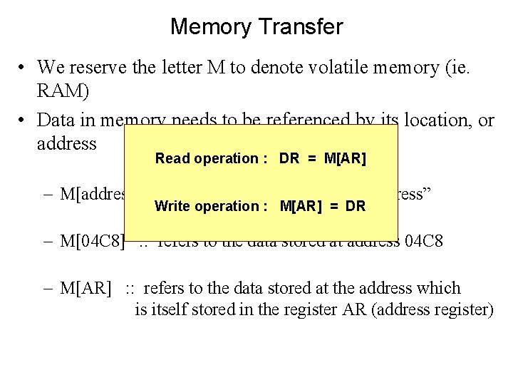
Memory Transfer • We reserve the letter M to denote volatile memory (ie. RAM) • Data in memory needs to be referenced by its location, or address Read operation : DR = M[AR] – M[address] : : refers to the data stored at “address” Write operation : M[AR] = DR – M[04 C 8] : : refers to the data stored at address 04 C 8 – M[AR] : : refers to the data stored at the address which is itself stored in the register AR (address register)
Microoperations Micro-operations are considered fundamental, or primitive (usually atomic) operations carried out in the CPU or elsewhere. 1. Register transfer microoperations transfer binary data from one register to another register. 2. Arithmetic microoperations perform arithmetic operations on numeric data stored in registers. 3. Logic microoperations perform bit manipulation operations on non-numeric data stored in registers. 4. Shift microoperations perform shift operations on data stored in registers.
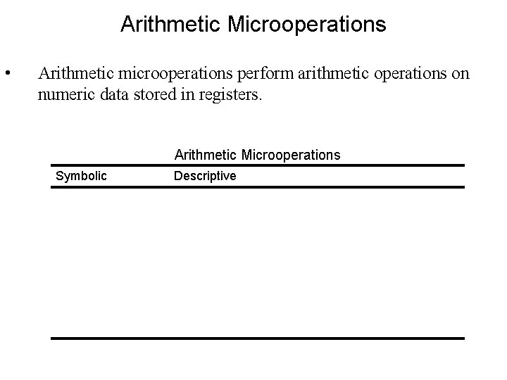
Arithmetic Microoperations • Arithmetic microoperations perform arithmetic operations on numeric data stored in registers. Arithmetic Microoperations Symbolic Descriptive R 3 = R 1 + R 2 Contents of R 1 plus R 2 transferred to R 3 = R 1 – R 2 Contents of R 1 minus R 2 transferred to R 3 R 1 = ~R 1 1’s complement the contents of R 1 R 2 = ~R 2 + 1 2’s complement the contents of R 2 (negate) R 3 = R 1 + ~R 2 + 1 R 1 plus 2’s complement of R 2 (subtraction) R 1 = R 1 + 1 Increment the contents of R 1 by one R 2 = R 2 – 1 Decrement the contents of R 2 by one
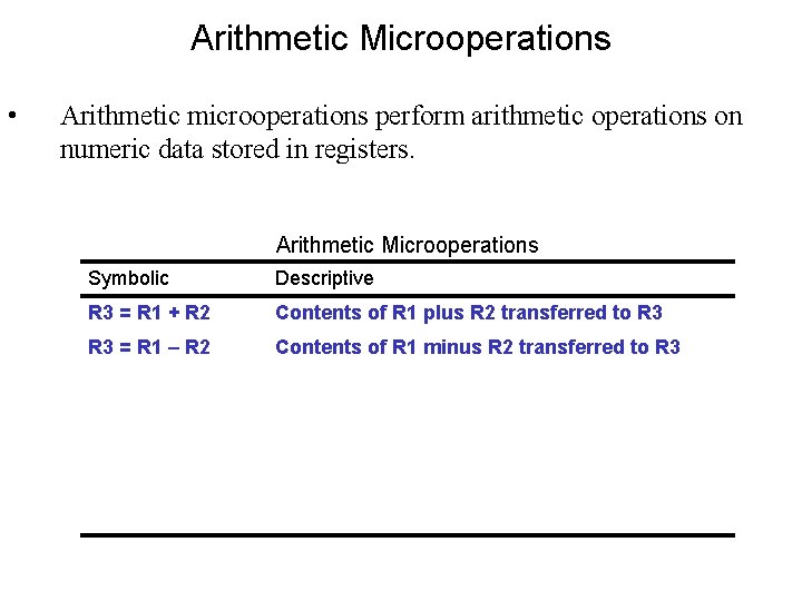
Arithmetic Microoperations • Arithmetic microoperations perform arithmetic operations on numeric data stored in registers. Arithmetic Microoperations Symbolic Descriptive R 3 = R 1 + R 2 Contents of R 1 plus R 2 transferred to R 3 = R 1 – R 2 Contents of R 1 minus R 2 transferred to R 3 R 1 = ~R 1 1’s complement the contents of R 1 R 2 = ~R 2 + 1 2’s complement the contents of R 2 (negate) R 3 = R 1 + ~R 2 + 1 R 1 plus 2’s complement of R 2 (subtraction) R 1 = R 1 + 1 Increment the contents of R 1 by one R 2 = R 2 – 1 Decrement the contents of R 2 by one
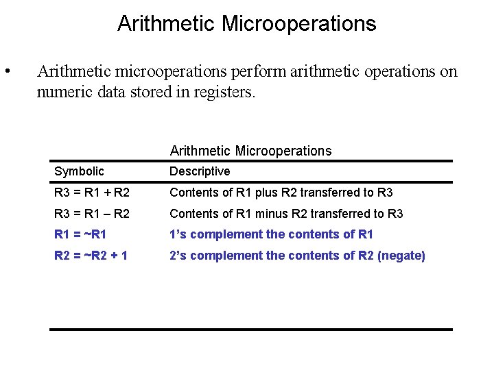
Arithmetic Microoperations • Arithmetic microoperations perform arithmetic operations on numeric data stored in registers. Arithmetic Microoperations Symbolic Descriptive R 3 = R 1 + R 2 Contents of R 1 plus R 2 transferred to R 3 = R 1 – R 2 Contents of R 1 minus R 2 transferred to R 3 R 1 = ~R 1 1’s complement the contents of R 1 R 2 = ~R 2 + 1 2’s complement the contents of R 2 (negate) R 3 = R 1 + ~R 2 + 1 R 1 plus 2’s complement of R 2 (subtraction) R 1 = R 1 + 1 Increment the contents of R 1 by one R 2 = R 2 – 1 Decrement the contents of R 2 by one
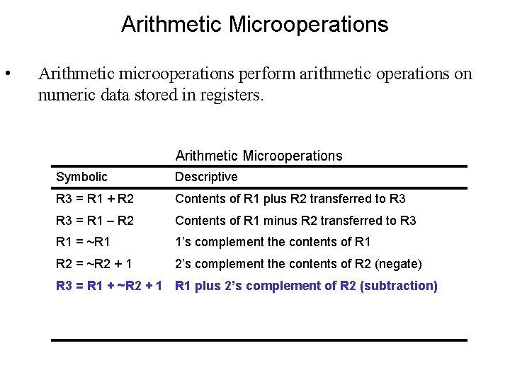
Arithmetic Microoperations • Arithmetic microoperations perform arithmetic operations on numeric data stored in registers. Arithmetic Microoperations Symbolic Descriptive R 3 = R 1 + R 2 Contents of R 1 plus R 2 transferred to R 3 = R 1 – R 2 Contents of R 1 minus R 2 transferred to R 3 R 1 = ~R 1 1’s complement the contents of R 1 R 2 = ~R 2 + 1 2’s complement the contents of R 2 (negate) R 3 = R 1 + ~R 2 + 1 R 1 plus 2’s complement of R 2 (subtraction) R 1 = R 1 + 1 Increment the contents of R 1 by one R 2 = R 2 – 1 Decrement the contents of R 2 by one
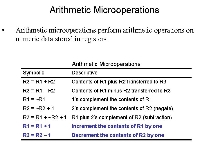
Arithmetic Microoperations • Arithmetic microoperations perform arithmetic operations on numeric data stored in registers. Arithmetic Microoperations Symbolic Descriptive R 3 = R 1 + R 2 Contents of R 1 plus R 2 transferred to R 3 = R 1 – R 2 Contents of R 1 minus R 2 transferred to R 3 R 1 = ~R 1 1’s complement the contents of R 1 R 2 = ~R 2 + 1 2’s complement the contents of R 2 (negate) R 3 = R 1 + ~R 2 + 1 R 1 plus 2’s complement of R 2 (subtraction) R 1 = R 1 + 1 Increment the contents of R 1 by one R 2 = R 2 – 1 Decrement the contents of R 2 by one
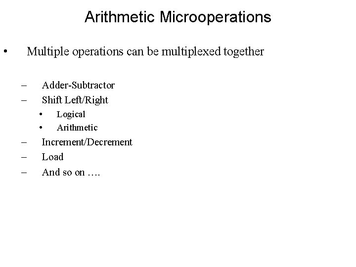
Arithmetic Microoperations • Multiple operations can be multiplexed together – – Adder-Subtractor Shift Left/Right • • – – – Logical Arithmetic Increment/Decrement Load And so on ….
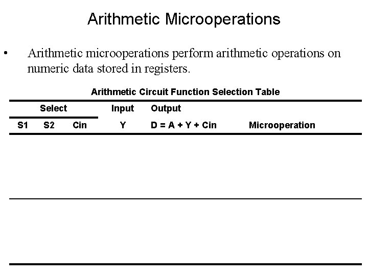
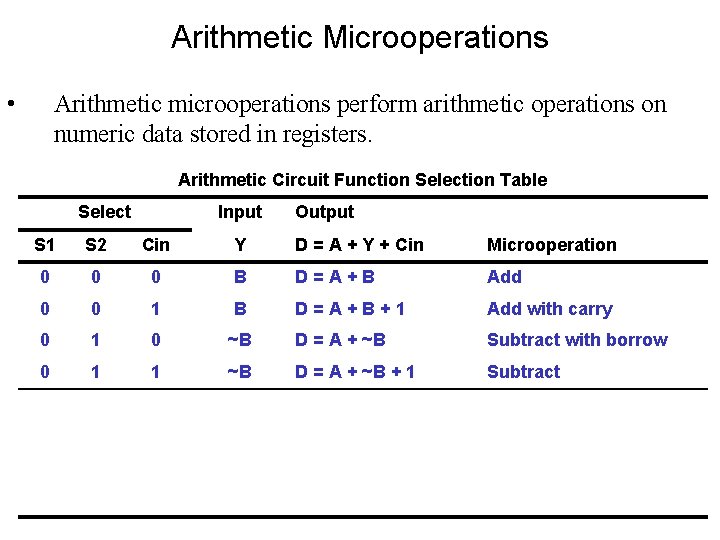
Arithmetic Microoperations • Arithmetic microoperations perform arithmetic operations on numeric data stored in registers. Arithmetic Circuit Function Selection Table Select Input Output S 1 S 2 Cin Y D = A + Y + Cin Microoperation 0 0 0 B D=A+B Add 0 0 1 B D=A+B+1 Add with carry 0 1 0 ~B D = A + ~B Subtract with borrow 0 1 1 ~B D = A + ~B + 1 Subtract 1 0 0 0 D=A Transfer A 1 0 D=A+1 Increment A 1 1 0 1 D=A-1 Decrement A 1 1 D=A Transfer A
Arithmetic Microoperations • Arithmetic microoperations perform arithmetic operations on numeric data stored in registers. Arithmetic Circuit Function Selection Table Select Input Output S 1 S 2 Cin Y D = A + Y + Cin Microoperation 0 0 0 B D=A+B Add 0 0 1 B D=A+B+1 Add with carry 0 1 0 ~B D = A + ~B Subtract with borrow 0 1 1 ~B D = A + ~B + 1 Subtract 1 0 0 0 D=A Transfer A 1 0 D=A+1 Increment A 1 1 0 1 D=A-1 Decrement A 1 1 D=A Transfer A
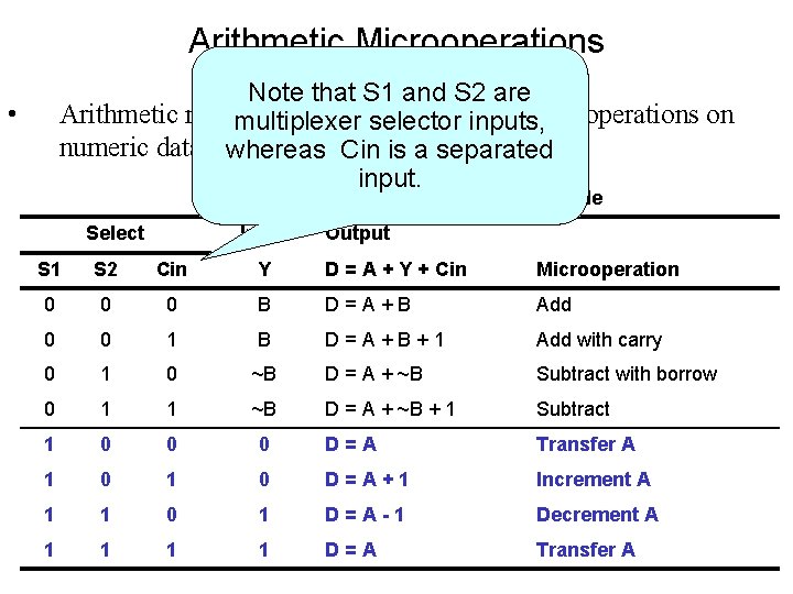
Arithmetic Microoperations Note that S 1 and S 2 are Arithmetic microoperations perform arithmetic multiplexer selector inputs, operations on numeric data stored in registers. whereas Cin is a separated input. • Arithmetic Circuit Function Selection Table Select Input Output S 1 S 2 Cin Y D = A + Y + Cin Microoperation 0 0 0 B D=A+B Add 0 0 1 B D=A+B+1 Add with carry 0 1 0 ~B D = A + ~B Subtract with borrow 0 1 1 ~B D = A + ~B + 1 Subtract 1 0 0 0 D=A Transfer A 1 0 D=A+1 Increment A 1 1 0 1 D=A-1 Decrement A 1 1 D=A Transfer A
Logic Microoperations • Logic microoperations perform bit manipulation operations on non-numeric data stored in registers.
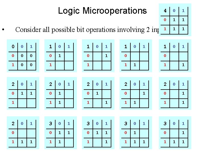
Logic Microoperations • 4 0 1 1 1 1 0 1 1 Consider all possible bit operations involving 2 inputs 0 0 1 1 0 0 1 2 0 0 1 1 0 1 2 0 1 1 1 0 1 1 2 0 1 1 1 1 3 0 1 1 0 1 1 2 0 0 1 1 1 0 1 3 0 1 1 1 1 1 2 1 0 1 1 3 0 0 0 1 1 1 1
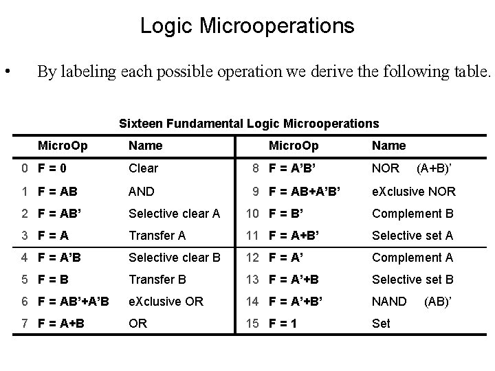
Logic Microoperations • By labeling each possible operation we derive the following table. Sixteen Fundamental Logic Microoperations Micro. Op Name 0 F=0 Clear 8 F = A’B’ NOR (A+B)’ 1 F = AB AND 9 F = AB+A’B’ e. Xclusive NOR 2 F = AB’ Selective clear A 10 F = B’ Complement B 3 F=A Transfer A 11 F = A+B’ Selective set A 4 F = A’B Selective clear B 12 F = A’ Complement A 5 F=B Transfer B 13 F = A’+B Selective set B 6 F = AB’+A’B e. Xclusive OR 14 F = A’+B’ NAND 7 F = A+B OR 15 F = 1 Set (AB)’
Logic Microoperations • Refer to Mano – Multiplexed Logic Circuit (Figure 4. 10) – Applications discussion, pages 11 -113
Shift Microoperations • Shift microoperations perform shift operations on data stored in registers. Shift Microoperations Symbolic Descriptive R = shl R Shift-left logical register R R = shr R Shift-right logical register R R = cil R Circular shift-left register R R = cir R Circular shift-right register R R = ashl R Shift-left arithmetic register R R = ashr R Shift-right arithmetic register R
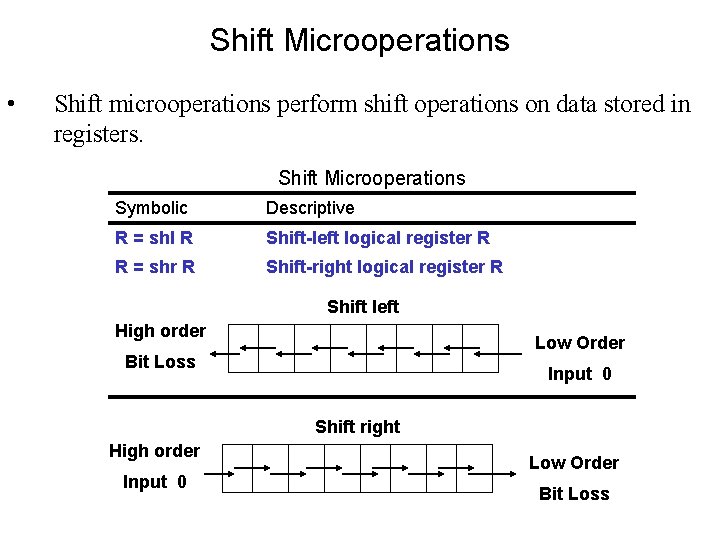
Shift Microoperations • Shift microoperations perform shift operations on data stored in registers. Shift Microoperations Symbolic Descriptive R = shl R Shift-left logical register R R = shr R Shift-right logical register R R = cil R Circular shift-left register R Shift left Circular shift-right register R R = cirorder R High RBit = ashl R Loss R = ashr R Shift-left arithmetic register R Shift-right arithmetic register R Low Order Input 0 Shift right High order Input 0 Low Order Bit Loss
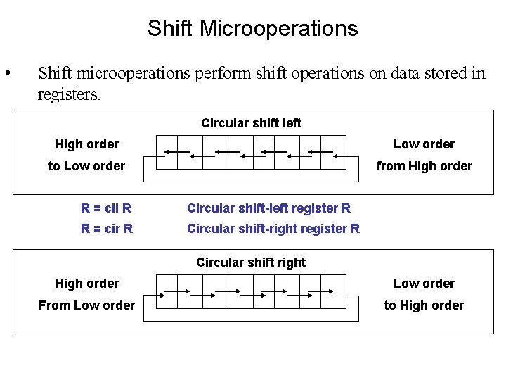
Shift Microoperations • Shift microoperations perform shift operations on data stored in registers. Circular shift left Shift Microoperations High. Symbolic order to Low R order = shl R Descriptive Shift-left logical register R R = shr R Shift-right logical register R R = cil R Circular shift-left register R R = cir R Circular shift-right register R R = ashl R Shift-left arithmetic register R Circular shift right Shift-right arithmetic register R R = ashr R High order From Low order from High order Low order to High order
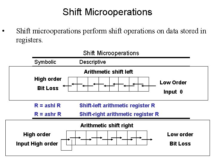
Shift Microoperations • Shift microoperations perform shift operations on data stored in registers. Shift Microoperations Symbolic Descriptive R = shl R High order R = shr R Shift-left logical register Arithmetic shift left R Shift-right logical register R Loss RBit = cil R Circular shift-left register R R = cir R Circular shift-right register R R = ashl R Shift-left arithmetic register R R = ashr R Shift-right arithmetic register R Low Order Input 0 Arithmetic shift right High order Low order Input High order Bit Loss
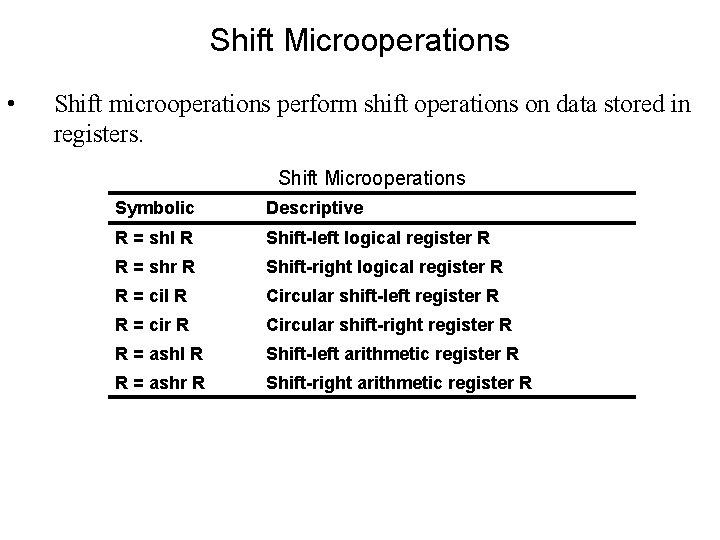
Shift Microoperations • Shift microoperations perform shift operations on data stored in registers. Shift Microoperations Symbolic Descriptive R = shl R Shift-left logical register R R = shr R Shift-right logical register R R = cil R Circular shift-left register R R = cir R Circular shift-right register R R = ashl R Shift-left arithmetic register R R = ashr R Shift-right arithmetic register R
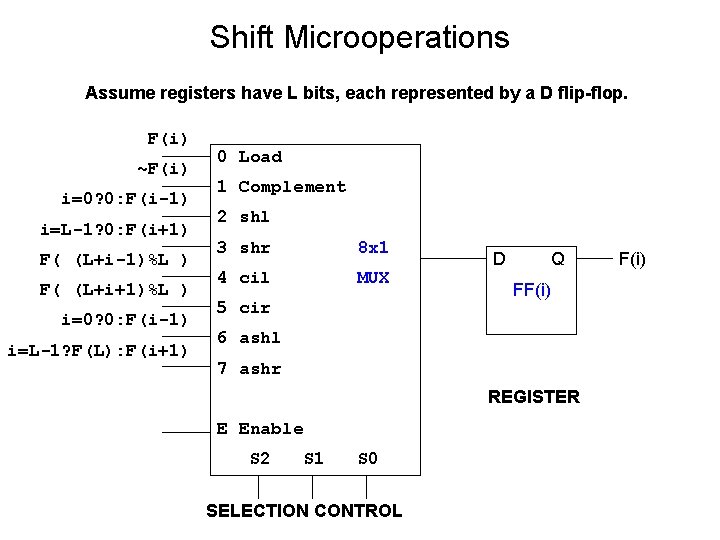
Shift Microoperations Assume registers have L bits, each represented by a D flip-flop. F(i) ~F(i) i=0? 0: F(i-1) i=L-1? 0: F(i+1) F( (L+i-1)%L ) F( (L+i+1)%L ) i=0? 0: F(i-1) i=L-1? F(L): F(i+1) 0 Load 1 Complement 2 shl 3 shr 8 x 1 4 cil MUX 5 cir D Q FF(i) 6 ashl 7 ashr REGISTER E Enable S 2 S 1 S 0 SELECTION CONTROL F(i)
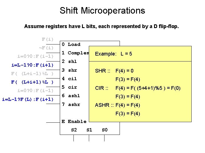
Shift Microoperations Assume registers have L bits, each represented by a D flip-flop. F(i) ~F(i) i=0? 0: F(i-1) i=L-1? 0: F(i+1) F( (L+i-1)%L ) F( (L+i+1)%L ) i=0? 0: F(i-1) i=L-1? F(L): F(i+1) 0 Load 1 Complement Example: L = 5 2 shl 3 shr 4 cil 3 x 8 SHR : : F(4) = 0 D DEC F(3) = F(4) 5 cir CIR : : F(3) = F(4) 7 ashr ASHR : : F(4) = F(4) F(3) = F(4) S 2 S 1 S 0 F(i) F(4) = F( (5+4+1)%5 ) = F(0) 6 ashl E Enable Q
Arithmetic Logic Shift Unit • Mano discusses a multi-stage circuit – Arithmetic stage – Logic stage – Multiplexed selection of operation • Read – Accompanying text
More Advanced Microoperations • The following topics are discussed later in Mano (3 d Edition Chapters 6 -10) and will be studied in the course 60 -460 (Advanced Architecture). – Integer Multiplication & Division – Floating Point Architectures • FP Register design • FP Microoperations – Input/Output Architectures • The discussion in the lecture is oral and conceptual. There are no points discussed that are important for examinations – this is optional material that will not be tested.
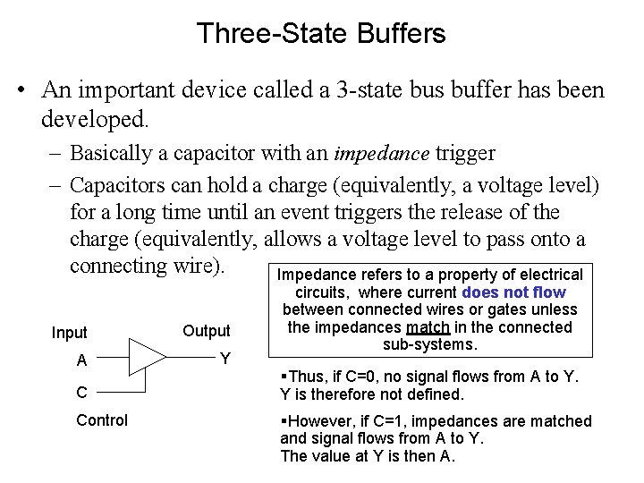
Three-State Buffers • An important device called a 3 -state bus buffer has been developed. – Basically a capacitor with an impedance trigger – Capacitors can hold a charge (equivalently, a voltage level) for a long time until an event triggers the release of the charge (equivalently, allows a voltage level to pass onto a connecting wire). Impedance refers to a property of electrical Input Output A Y C Control circuits, where current does not flow between connected wires or gates unless the impedances match in the connected sub-systems. §Thus, if C=0, no signal flows from A to Y. Y is therefore not defined. §However, if C=1, impedances are matched and signal flows from A to Y. The value at Y is then A.
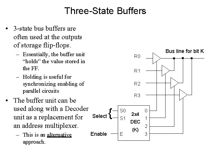
Three-State Buffers • 3 -state bus buffers are often used at the outputs of storage flip-flops. – Essentially, the buffer unit “holds” the value stored in the FF. – Holding is useful for synchronizing enabling of parallel circuits • The buffer unit can be used along with a Decoder unit as a replacement for an address multiplexer. – This is an alternative approach. Bus line for bit K R 0 R 1 R 2 R 3 Select Enable { S 0 S 1 E 2 x 4 DEC (K) 0 1 2 3
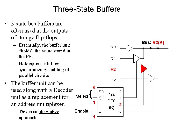
Three-State Buffers • 3 -state bus buffers are often used at the outputs of storage flip-flops. – Essentially, the buffer unit “holds” the value stored in the FF. – Holding is useful for synchronizing enabling of parallel circuits • The buffer unit can be used along with a Decoder unit as a replacement for an address multiplexer. – This is an alternative approach. Bus: R 2(K) R 0 R 1 R 2 R 3 Select { 0 1 Enable S 0 S 1 E 1 2 x 4 DEC (K) 0 1 2 3
Summary • We introduced Mano’s basic CPU architecture – Registers – Bus • We discussed Register and Memory Transfer and introduced a language suitable for description and design • We presented several example applications of RTL/MTL for Microoperations – Arithmetic – Logic – Shift • We discussed briefly more advanced applications
- Slides: 46