Computer Architecture ECE 361 Lecture 7 ALU Design
- Slides: 17

Computer Architecture ECE 361 Lecture 7: ALU Design : Division 361 div. 1

Outline of Today’s Lecture ° Introduction to Today’s Lecture ° Divide ° Questions and Administrative Matters ° Introduction to Single cycle processor design 361 div. 2

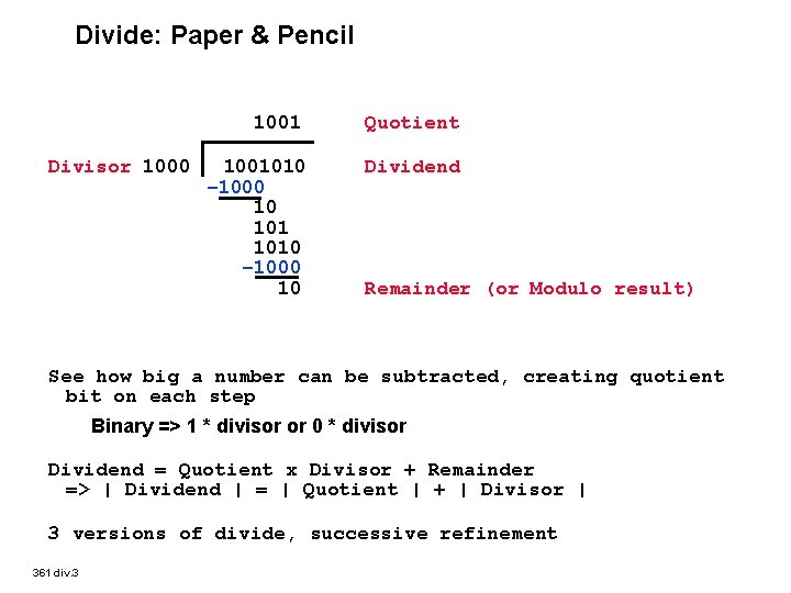
Divide: Paper & Pencil Divisor 1000 1001 Quotient 1001010 – 1000 10 Dividend Remainder (or Modulo result) See how big a number can be subtracted, creating quotient bit on each step Binary => 1 * divisor or 0 * divisor Dividend = Quotient x Divisor + Remainder => | Dividend | = | Quotient | + | Divisor | 3 versions of divide, successive refinement 361 div. 3

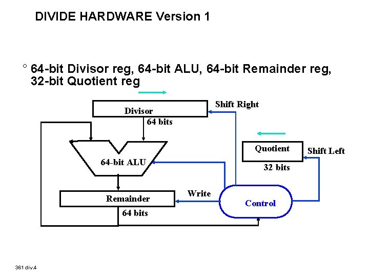
DIVIDE HARDWARE Version 1 ° 64 -bit Divisor reg, 64 -bit ALU, 64 -bit Remainder reg, 32 -bit Quotient reg Shift Right Divisor 64 bits Quotient 64 -bit ALU Remainder 64 bits 361 div. 4 32 bits Write Control Shift Left

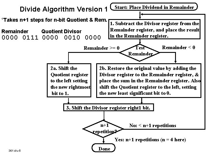
Start: Place Dividend in Remainder Divide Algorithm Version 1 °Takes n+1 steps for n-bit Quotient & Remainder Quotient Divisor 0000 0111 0000 0010 0000 1. Subtract the Divisor register from the Remainder register, and place the result in the Remainder register. Remainder >= 0 2 a. Shift the Quotient register to the left setting the new rightmost bit to 1. Test Remainder < 0 2 b. Restore the original value by adding the Divisor register to the Remainder register, & place the sum in the Remainder register. Also shift the Quotient register to the left, setting the new least significant bit to 0. 3. Shift the Divisor register right 1 bit. n+1 repetition? No: < n+1 repetitions Yes: n+1 repetitions (n = 4 here) 361 div. 5 Done

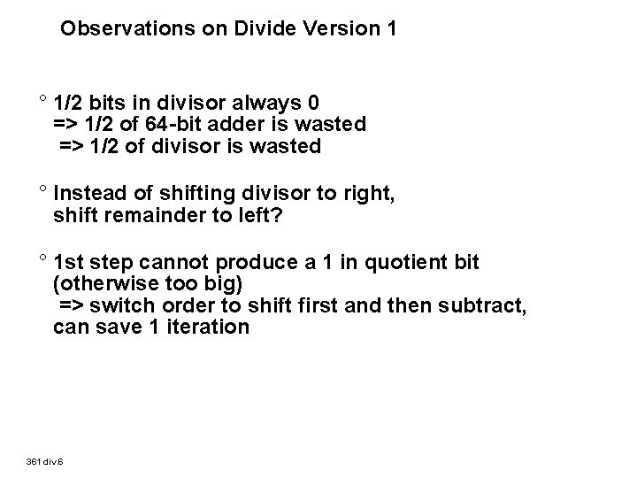
Observations on Divide Version 1 ° 1/2 bits in divisor always 0 => 1/2 of 64 -bit adder is wasted => 1/2 of divisor is wasted ° Instead of shifting divisor to right, shift remainder to left? ° 1 st step cannot produce a 1 in quotient bit (otherwise too big) => switch order to shift first and then subtract, can save 1 iteration 361 div. 6

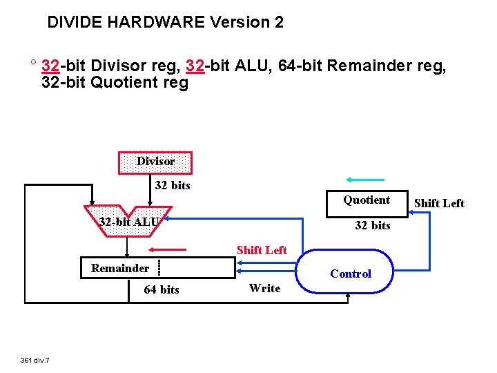
DIVIDE HARDWARE Version 2 ° 32 -bit Divisor reg, 32 -bit ALU, 64 -bit Remainder reg, 32 -bit Quotient reg Divisor 32 bits Quotient 32 -bit ALU 32 bits Shift Left Remainder 64 bits 361 div. 7 Control Write Shift Left

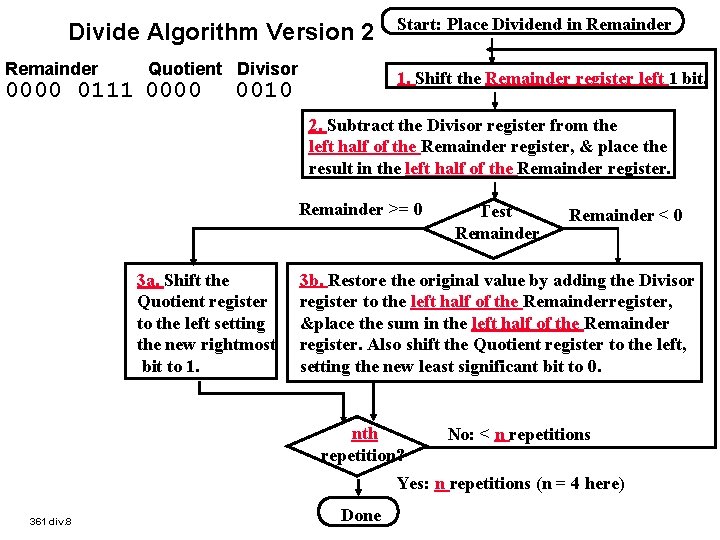
Divide Algorithm Version 2 Remainder Quotient Divisor 0000 0111 0000 Start: Place Dividend in Remainder 1. Shift the Remainder register left 1 bit. 0010 2. Subtract the Divisor register from the left half of the Remainder register, & place the result in the left half of the Remainder register. Remainder >= 0 3 a. Shift the Quotient register to the left setting the new rightmost bit to 1. Test Remainder < 0 3 b. Restore the original value by adding the Divisor register to the left half of the Remainderregister, &place the sum in the left half of the Remainder register. Also shift the Quotient register to the left, setting the new least significant bit to 0. nth repetition? No: < n repetitions Yes: n repetitions (n = 4 here) 361 div. 8 Done

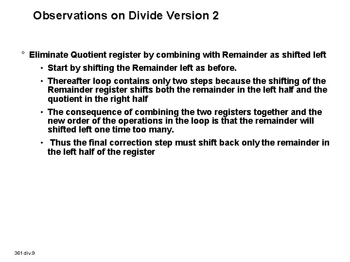
Observations on Divide Version 2 ° Eliminate Quotient register by combining with Remainder as shifted left • Start by shifting the Remainder left as before. • Thereafter loop contains only two steps because the shifting of the Remainder register shifts both the remainder in the left half and the quotient in the right half • The consequence of combining the two registers together and the new order of the operations in the loop is that the remainder will shifted left one time too many. • Thus the final correction step must shift back only the remainder in the left half of the register 361 div. 9

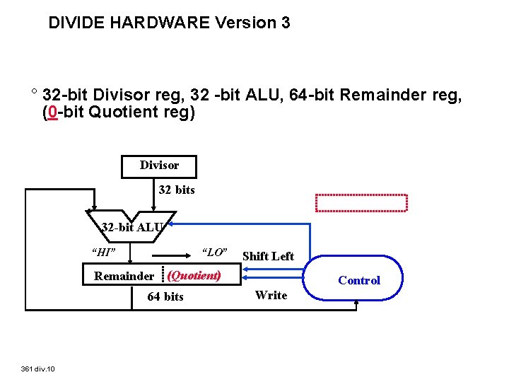
DIVIDE HARDWARE Version 3 ° 32 -bit Divisor reg, 32 -bit ALU, 64 -bit Remainder reg, (0 -bit Quotient reg) Divisor 32 bits 32 -bit ALU “HI” “LO” Shift Left Remainder (Quotient) 64 bits 361 div. 10 Control Write

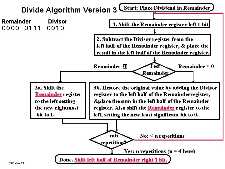
Divide Algorithm Version 3 Remainder Divisor 0000 0111 0010 Start: Place Dividend in Remainder 1. Shift the Remainder register left 1 bit. 2. Subtract the Divisor register from the left half of the Remainder register, & place the result in the left half of the Remainder register. Remainder � 0 3 a. Shift the Remainder register to the left setting the new rightmost bit to 1. Test Remainder < 0 3 b. Restore the original value by adding the Divisor register to the left half of the Remainderregister, &place the sum in the left half of the Remainder register. Also shift the Remainder register to the left, setting the new least significant bit to 0. nth repetition? No: < n repetitions Yes: n repetitions (n = 4 here) 361 div. 11 Done. Shift left half of Remainder right 1 bit.

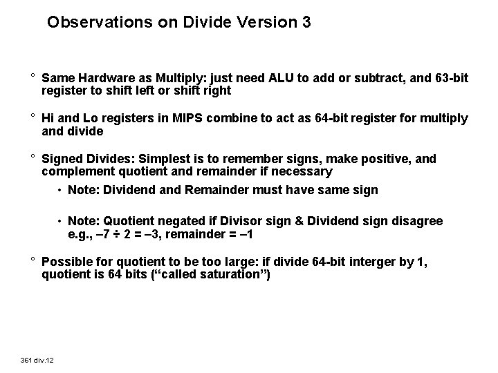
Observations on Divide Version 3 ° Same Hardware as Multiply: just need ALU to add or subtract, and 63 -bit register to shift left or shift right ° Hi and Lo registers in MIPS combine to act as 64 -bit register for multiply and divide ° Signed Divides: Simplest is to remember signs, make positive, and complement quotient and remainder if necessary • Note: Dividend and Remainder must have same sign • Note: Quotient negated if Divisor sign & Dividend sign disagree e. g. , – 7 ÷ 2 = – 3, remainder = – 1 ° Possible for quotient to be too large: if divide 64 -bit interger by 1, quotient is 64 bits (“called saturation”) 361 div. 12

Summary ° Bits have no inherent meaning: operations determine whether they are really ASCII characters, integers, floating point numbers ° Divide can use same hardware as multiply: Hi & Lo registers in MIPS 361 div. 13

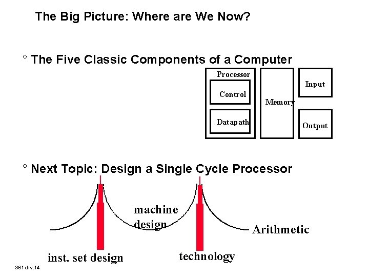
The Big Picture: Where are We Now? ° The Five Classic Components of a Computer Processor Input Control Memory Datapath Output ° Next Topic: Design a Single Cycle Processor machine design inst. set design 361 div. 14 Arithmetic technology

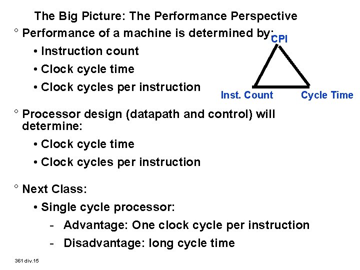
The Big Picture: The Performance Perspective ° Performance of a machine is determined by: CPI • Instruction count • Clock cycle time • Clock cycles per instruction Inst. Count Cycle Time ° Processor design (datapath and control) will determine: • Clock cycle time • Clock cycles per instruction ° Next Class: • Single cycle processor: - Advantage: One clock cycle per instruction - Disadvantage: long cycle time 361 div. 15

How to Design a Processor: step-by-step ° 1. Analyze instruction set => datapath requirements • the meaning of each instruction is given by the register transfers • datapath must include storage element for ISA registers - possibly more • datapath must support each register transfer ° 2. Select set of datapath components and establish clocking methodology ° 3. Assemble datapath meeting the requirements ° 4. Analyze implementation of each instruction to determine setting of control points that effects the register transfer. ° 5. Assemble the control logic 361 div. 16

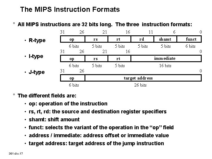
The MIPS Instruction Formats ° All MIPS instructions are 32 bits long. The three instruction formats: 31 26 op • R-type rs 6 bits • I-type • J-type 31 21 op 6 bits 31 rt 5 bits 26 16 5 bits 21 rs 5 bits 11 6 rd shamt funct 5 bits 6 bits 16 rt 5 bits 0 immediate 16 bits 26 op 6 bits 0 target address 26 bits ° The different fields are: • op: operation of the instruction • rs, rt, rd: the source and destination register specifiers • shamt: shift amount • funct: selects the variant of the operation in the “op” field • address / immediate: address offset or immediate value • target address: target address of the jump instruction 361 div. 17 0