COMPUTER ARCHITECTURE CS 6354 Emerging Memory Technologies Samira


- Slides: 44

COMPUTER ARCHITECTURE CS 6354 Emerging Memory Technologies Samira Khan University of Virginia Oct 23, 2017 The content and concept of this course are adapted from CMU ECE 740

AGENDA • Logistics • Review from last lecture • Emerging Memory Technology 2

LOGISTICS • Review due this Wednesday – Scalable high performance main memory system using phase-change Memory Technology, ISCA 2009 – 3 D-Stacked Memory Architectures for Multi-core Processors, ISCA 2008 • Exam papers – Pick up from Marzieh during her office hour • Milestone slides due Nov 1 – No class on Nov 1, please work on your project – I will assign time slots to meet in my office during Nov 2, 3, 6 3

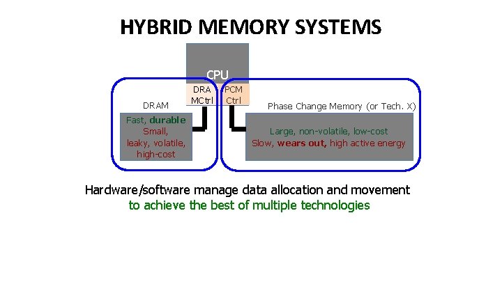
SOLUTIONS TO THE DRAM SCALING PROBLEM • Two potential solutions – Tolerate DRAM (by taking a fresh look at it) – Enable emerging memory technologies to eliminate/minimize DRAM • Do both – Hybrid memory systems 4

SOLUTIONS TO THE DRAM SCALING PROBLEM • Two potential solutions – Tolerate DRAM (by taking a fresh look at it) – Enable emerging memory technologies to eliminate/minimize DRAM • Do both – Hybrid memory systems 5

SOLUTION 2: EMERGING MEMORY TECHNOLOGIES • Some emerging resistive memory technologies seem more scalable than DRAM (and they are non-volatile) • Example: Phase Change Memory – Expected to scale to 9 nm (2022 [ITRS]) – Expected to be denser than DRAM: can store multiple bits/cell • But, emerging technologies have shortcomings as well – Can they be enabled to replace/augment/surpass DRAM? 6

HYBRID MEMORY SYSTEMS CPU DRAM Fast, durable Small, leaky, volatile, high-cost DRA MCtrl PCM Ctrl Phase Change Memory (or Tech. X) Large, non-volatile, low-cost Slow, wears out, high active energy Hardware/software manage data allocation and movement to achieve the best of multiple technologies

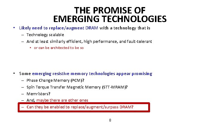
THE PROMISE OF EMERGING TECHNOLOGIES • Likely need to replace/augment DRAM with a technology that is – Technology scalable – And at least similarly efficient, high performance, and fault-tolerant • or can be architected to be so • Some emerging resistive memory technologies appear promising – – – Phase Change Memory (PCM)? Spin Torque Transfer Magnetic Memory (STT-MRAM)? Memristors? And, maybe there are other ones Can they be enabled to replace/augment/surpass DRAM? 8

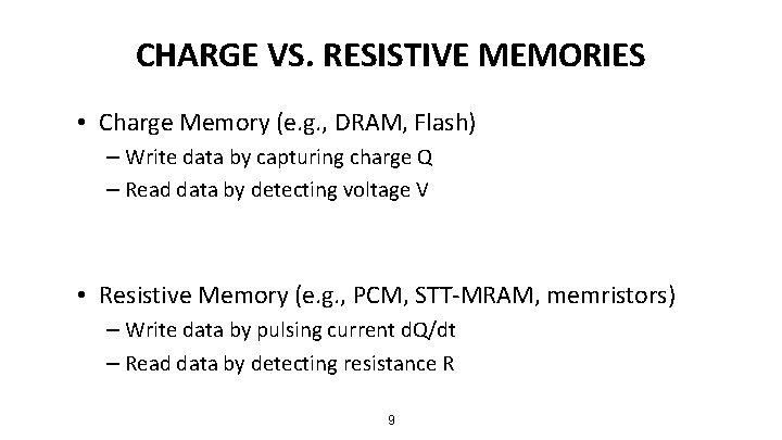
CHARGE VS. RESISTIVE MEMORIES • Charge Memory (e. g. , DRAM, Flash) – Write data by capturing charge Q – Read data by detecting voltage V • Resistive Memory (e. g. , PCM, STT-MRAM, memristors) – Write data by pulsing current d. Q/dt – Read data by detecting resistance R 9

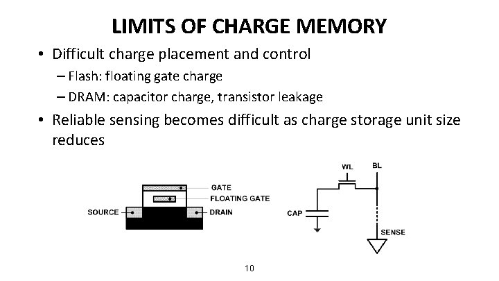
LIMITS OF CHARGE MEMORY • Difficult charge placement and control – Flash: floating gate charge – DRAM: capacitor charge, transistor leakage • Reliable sensing becomes difficult as charge storage unit size reduces 10

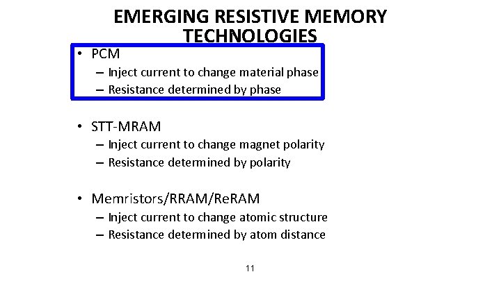
EMERGING RESISTIVE MEMORY TECHNOLOGIES • PCM – Inject current to change material phase – Resistance determined by phase • STT-MRAM – Inject current to change magnet polarity – Resistance determined by polarity • Memristors/RRAM/Re. RAM – Inject current to change atomic structure – Resistance determined by atom distance 11

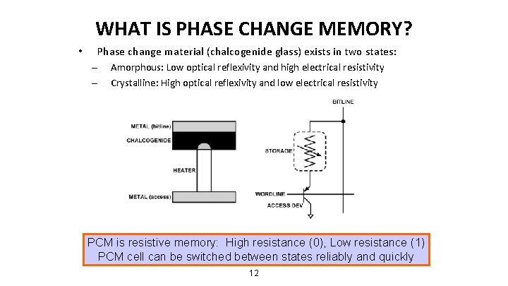
WHAT IS PHASE CHANGE MEMORY? • Phase change material (chalcogenide glass) exists in two states: – – Amorphous: Low optical reflexivity and high electrical resistivity Crystalline: High optical reflexivity and low electrical resistivity PCM is resistive memory: High resistance (0), Low resistance (1) PCM cell can be switched between states reliably and quickly 12

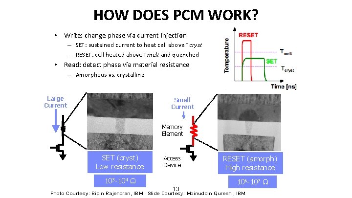
HOW DOES PCM WORK? • Write: change phase via current injection – SET: sustained current to heat cell above Tcryst – RESET: cell heated above Tmelt and quenched • Read: detect phase via material resistance – Amorphous vs. crystalline Large Current Small Current Memory Element SET (cryst) Low resistance Access Device 103 -104 W 13 RESET (amorph) High resistance 106 -107 W Photo Courtesy: Bipin Rajendran, IBM Slide Courtesy: Moinuddin Qureshi, IBM

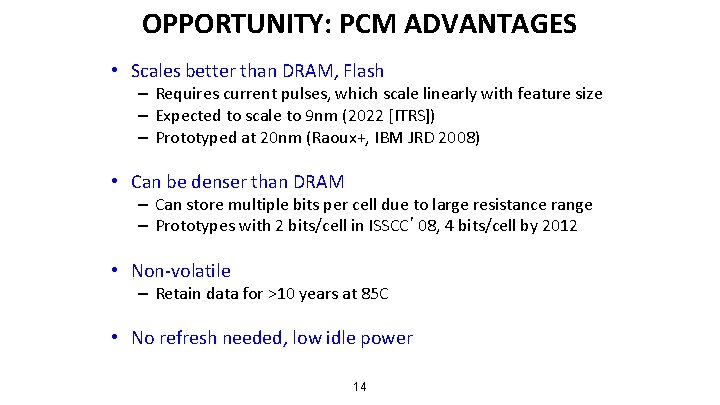
OPPORTUNITY: PCM ADVANTAGES • Scales better than DRAM, Flash – Requires current pulses, which scale linearly with feature size – Expected to scale to 9 nm (2022 [ITRS]) – Prototyped at 20 nm (Raoux+, IBM JRD 2008) • Can be denser than DRAM – Can store multiple bits per cell due to large resistance range – Prototypes with 2 bits/cell in ISSCC’ 08, 4 bits/cell by 2012 • Non-volatile – Retain data for >10 years at 85 C • No refresh needed, low idle power 14

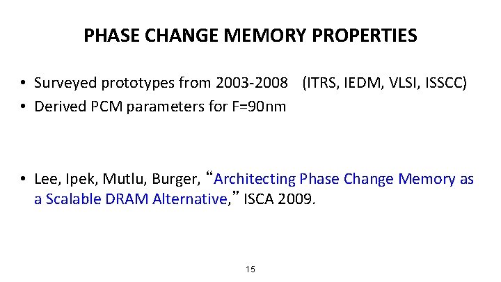
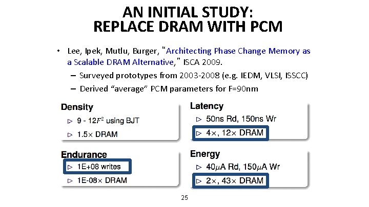
PHASE CHANGE MEMORY PROPERTIES • Surveyed prototypes from 2003 -2008 (ITRS, IEDM, VLSI, ISSCC) • Derived PCM parameters for F=90 nm • Lee, Ipek, Mutlu, Burger, “Architecting Phase Change Memory as a Scalable DRAM Alternative, ” ISCA 2009. 15

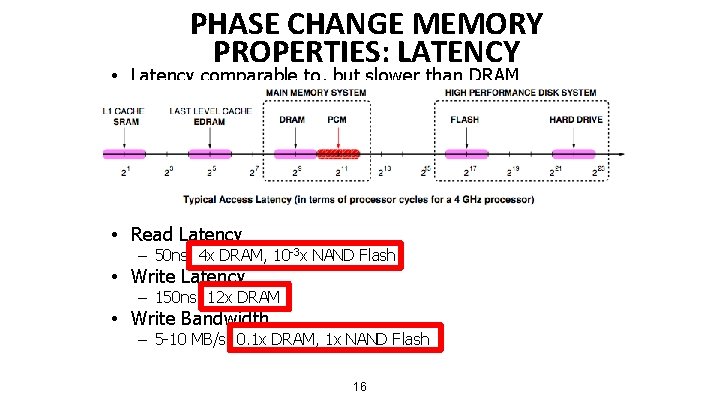
PHASE CHANGE MEMORY PROPERTIES: LATENCY • Latency comparable to, but slower than DRAM • Read Latency – 50 ns: 4 x DRAM, 10 -3 x NAND Flash • Write Latency – 150 ns: 12 x DRAM • Write Bandwidth – 5 -10 MB/s: 0. 1 x DRAM, 1 x NAND Flash 16

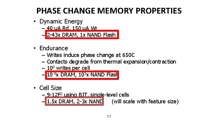
PHASE CHANGE MEMORY PROPERTIES • Dynamic Energy – 40 u. A Rd, 150 u. A Wr – 2 -43 x DRAM, 1 x NAND Flash • Endurance – – Writes induce phase change at 650 C Contacts degrade from thermal expansion/contraction 108 writes per cell 10 -8 x DRAM, 103 x NAND Flash • Cell Size – 9 -12 F 2 using BJT, single-level cells – 1. 5 x DRAM, 2 -3 x NAND (will scale with feature size) 17

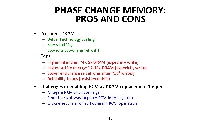
PHASE CHANGE MEMORY: PROS AND CONS • Pros over DRAM – Better technology scaling – Non volatility – Low idle power (no refresh) • Cons – – Higher latencies: ~4 -15 x DRAM (especially write) Higher active energy: ~2 -50 x DRAM (especially write) Lower endurance (a cell dies after ~108 writes) Reliability issues (resistance drift) • Challenges in enabling PCM as DRAM replacement/helper: – Mitigate PCM shortcomings – Find the right way to place PCM in the system – Ensure secure and fault-tolerant PCM operation 18

PCM-BASED MAIN MEMORY: SOME QUESTIONS • Where to place PCM in the memory hierarchy? – Hybrid OS controlled PCM-DRAM – Hybrid OS controlled PCM and hardware-controlled DRAM – Pure PCM main memory • How to mitigate shortcomings of PCM? • How to take advantage of (byte-addressable and fast) non-volatile main memory? 19

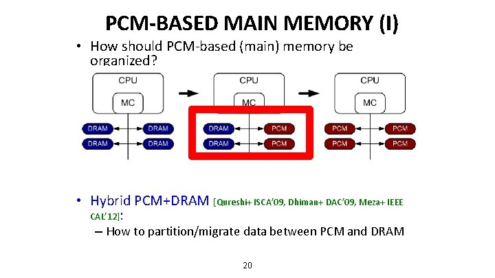
PCM-BASED MAIN MEMORY (I) • How should PCM-based (main) memory be organized? • Hybrid PCM+DRAM [Qureshi+ ISCA’ 09, Dhiman+ DAC’ 09, Meza+ IEEE CAL’ 12]: – How to partition/migrate data between PCM and DRAM 20

HYBRID MEMORY SYSTEMS: CHALLENGES • Partitioning – Should DRAM be a cache or main memory, or configurable? – What fraction? How many controllers? • Data allocation/movement (energy, performance, lifetime) – Who manages allocation/movement? – What are good control algorithms? – How do we prevent degradation of service due to wearout? • Design of cache hierarchy, memory controllers, OS – Mitigate PCM shortcomings, exploit PCM advantages • Design of PCM/DRAM chips and modules – Rethink the design of PCM/DRAM with new requirements 21

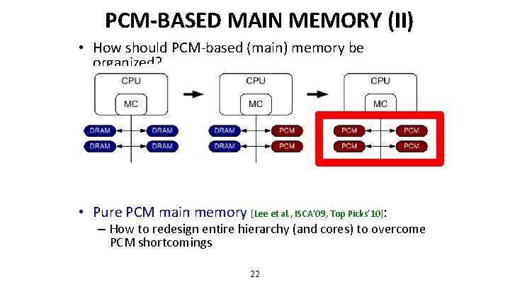
PCM-BASED MAIN MEMORY (II) • How should PCM-based (main) memory be organized? • Pure PCM main memory [Lee et al. , ISCA’ 09, Top Picks’ 10]: – How to redesign entire hierarchy (and cores) to overcome PCM shortcomings 22

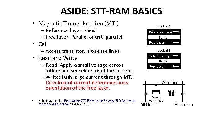
ASIDE: STT-RAM BASICS • Magnetic Tunnel Junction (MTJ) – Reference layer: Fixed – Free layer: Parallel or anti-parallel • Cell – Access transistor, bit/sense lines • Read and Write – Read: Apply a small voltage across bitline and senseline; read the current. – Write: Push large current through MTJ. Direction of current determines new orientation of the free layer. • Kultursay et al. , “Evaluating STT-RAM as an Energy-Efficient Main Memory Alternative, ” ISPASS 2013 Logical 0 Reference Layer Barrier Free Layer Logical 1 Reference Layer Barrier Free Layer Word Line MTJ Access Transistor Bit Line Sense Line

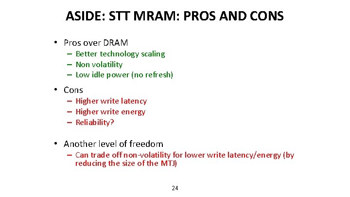
ASIDE: STT MRAM: PROS AND CONS • Pros over DRAM – Better technology scaling – Non volatility – Low idle power (no refresh) • Cons – Higher write latency – Higher write energy – Reliability? • Another level of freedom – Can trade off non-volatility for lower write latency/energy (by reducing the size of the MTJ) 24

AN INITIAL STUDY: REPLACE DRAM WITH PCM • Lee, Ipek, Mutlu, Burger, “Architecting Phase Change Memory as a Scalable DRAM Alternative, ” ISCA 2009. – Surveyed prototypes from 2003 -2008 (e. g. IEDM, VLSI, ISSCC) – Derived “average” PCM parameters for F=90 nm 25

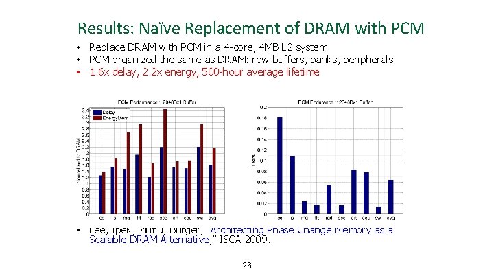
Results: Naïve Replacement of DRAM with PCM • Replace DRAM with PCM in a 4 -core, 4 MB L 2 system • PCM organized the same as DRAM: row buffers, banks, peripherals • 1. 6 x delay, 2. 2 x energy, 500 -hour average lifetime • Lee, Ipek, Mutlu, Burger, “Architecting Phase Change Memory as a Scalable DRAM Alternative, ” ISCA 2009. 26

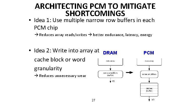
ARCHITECTING PCM TO MITIGATE SHORTCOMINGS • Idea 1: Use multiple narrow buffers in each PCM chip Reduces array reads/writes better endurance, latency, energy • Idea 2: Write into array at cache block or word granularity Reduces unnecessary wear 27 DRAM PCM

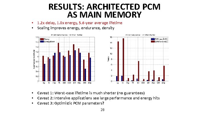
RESULTS: ARCHITECTED PCM AS MAIN MEMORY • 1. 2 x delay, 1. 0 x energy, 5. 6 -year average lifetime • Scaling improves energy, endurance, density • Caveat 1: Worst-case lifetime is much shorter (no guarantees) • Caveat 2: Intensive applications see large performance and energy hits • Caveat 3: Optimistic PCM parameters? 28

OTHER OPPORTUNITIES WITH EMERGING TECHNOLOGIES • Merging of memory and storage – e. g. , a single interface to manage all data • New applications – e. g. , ultra-fast checkpoint and restore • More robust system design – e. g. , reducing data loss • Processing tightly-coupled with memory – e. g. , enabling efficient search and filtering 29

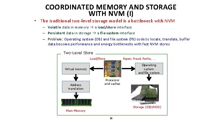
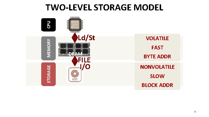
COORDINATED MEMORY AND STORAGE WITH NVM (I) • The traditional two-level storage model is a bottleneck with NVM – Volatile data in memory a load/store interface – Persistent data in storage a file system interface – Problem: Operating system (OS) and file system (FS) code to locate, translate, buffer data become performance and energy bottlenecks with fast NVM stores Two-Level Store Load/Store fopen, fread, fwrite, … Operating system and file system Virtual memory Address translation Processor and caches Storage (SSD/HDD) Main Memory 30

STORAGE MEMORY CPU TWO-LEVEL STORAGE MODEL Ld/St DRAM FILE I/O VOLATILE FAST BYTE ADDR NONVOLATILE SLOW BLOCK ADDR 31

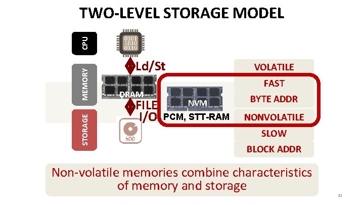
STORAGE MEMORY CPU TWO-LEVEL STORAGE MODEL Ld/St DRAM FILE I/O VOLATILE FAST NVM BYTE ADDR PCM, STT-RAM NONVOLATILE SLOW BLOCK ADDR Non-volatile memories combine characteristics of memory and storage 32

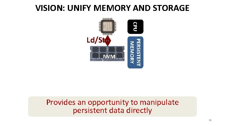
VISION: UNIFY MEMORY AND STORAGE CPU NVM PERSISTENT MEMORY Ld/St Provides an opportunity to manipulate persistent data directly 33

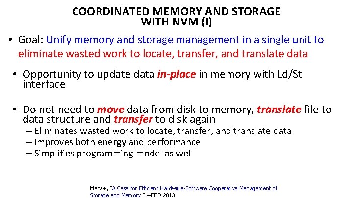
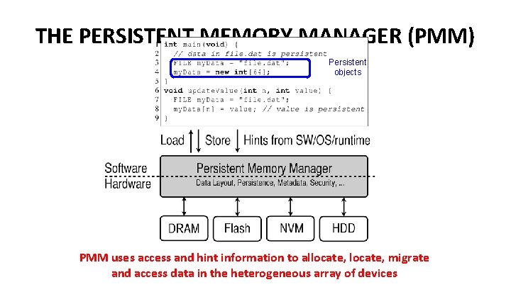
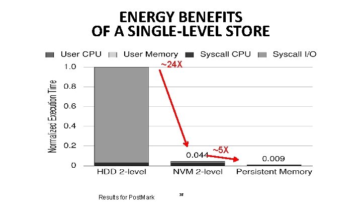
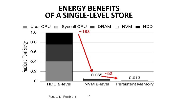
COORDINATED MEMORY AND STORAGE WITH NVM (I) • Goal: Unify memory and storage management in a single unit to eliminate wasted work to locate, transfer, and translate data • Opportunity to update data in-place in memory with Ld/St interface • Do not need to move data from disk to memory, translate file to data structure and transfer to disk again – Eliminates wasted work to locate, transfer, and translate data – Improves both energy and performance – Simplifies programming model as well 34 Meza+, “A Case for Efficient Hardware-Software Cooperative Management of Storage and Memory, ” WEED 2013.

THE PERSISTENT MEMORY MANAGER (PMM) Persistent objects PMM uses access and hint information to allocate, migrate 35 and access data in the heterogeneous array of devices

ENERGY BENEFITS OF A SINGLE-LEVEL STORE ~24 X ~5 X Results for Post. Mark 36

ENERGY BENEFITS OF A SINGLE-LEVEL STORE ~16 X ~5 X Results for Post. Mark 37

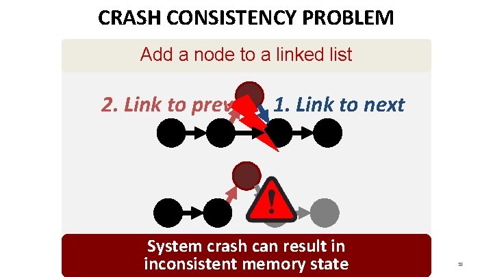
CRASH CONSISTENCY PROBLEM Add a node to a linked list 2. Link to prev 1. Link to next System crash can result in inconsistent memory state 38

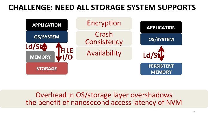
CHALLENGE: NEED ALL STORAGE SYSTEM SUPPORTS APPLICATION OS/SYSTEM Ld/St MEMORY STORAGE FILE I/O Encryption Crash Consistency NVM Availability APPLICATION OS/SYSTEM Ld/St PERSISTENT MEMORY Overhead in OS/storage layer overshadows the benefit of nanosecond access latency of NVM 39

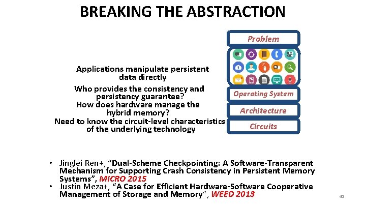
BREAKING THE ABSTRACTION Problem Applications manipulate persistent data directly Who provides the consistency and Operating System persistency guarantee? How does hardware manage the Architecture hybrid memory? Need to know the circuit-level characteristics Circuits of the underlying technology • Jinglei Ren+, “Dual-Scheme Checkpointing: A Software-Transparent Mechanism for Supporting Crash Consistency in Persistent Memory Systems”, MICRO 2015 • Justin Meza+, “A Case for Efficient Hardware-Software Cooperative Management of Storage and Memory”, WEED 2013 40

ENABLING AND EXPLOITING NVM: ISSUES • Many issues and ideas from technology layer to algorithms layer • Enabling NVM and hybrid memory – – How to tolerate errors? How to enable secure operation? How to tolerate performance and power shortcomings? How to minimize cost? • Exploiting emerging technologies – How to exploit non-volatility? – How to minimize energy consumption? – How to exploit NVM on chip? 41

THREE PRINCIPLES FOR (MEMORY) SCALING • Better cooperation between devices and the system – Expose more information about devices to upper layers – More flexible interfaces • Better-than-worst-case design – Do not optimize for the worst case – Worst case should not determine the common case • Heterogeneity in design (specialization, asymmetry) – Enables a more efficient design (No one size fits all) • These principles are related and sometimes coupled 42

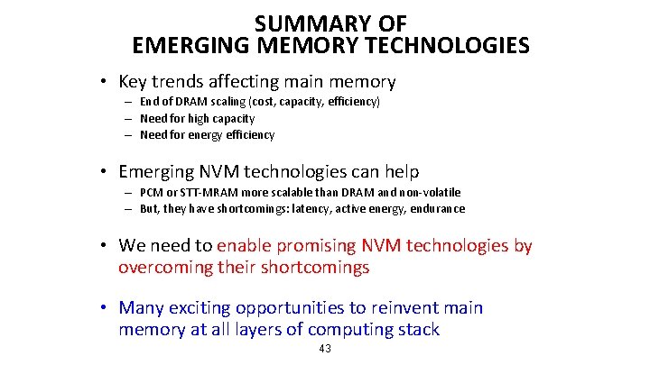
SUMMARY OF EMERGING MEMORY TECHNOLOGIES • Key trends affecting main memory – End of DRAM scaling (cost, capacity, efficiency) – Need for high capacity – Need for energy efficiency • Emerging NVM technologies can help – PCM or STT-MRAM more scalable than DRAM and non-volatile – But, they have shortcomings: latency, active energy, endurance • We need to enable promising NVM technologies by overcoming their shortcomings • Many exciting opportunities to reinvent main memory at all layers of computing stack 43

COMPUTER ARCHITECTURE CS 6354 Emerging Memory Technologies Samira Khan University of Virginia Oct 23, 2017 The content and concept of this course are adapted from CMU ECE 740