Computer Architecture Chapter Three Digital Components This process
- Slides: 16

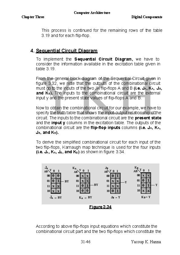
Computer Architecture Chapter Three Digital Components This process is continued for the remaining rows of the table 3. 19 and for each flip-flop. 4. Sequential Circuit Diagram To implement the Sequential Circuit Diagram, we have to consider the information available in the excitation table given in table 3. 19. From the general block diagram of the Sequential Circuit given in figure 3. 32, we note that the outputs of the combinational circuit must go to the inputs of the two JK flip-flops A and B (i. e. JA, KA, JB, and KB). The inputs to the combinational circuit are the external input y and the present state values of flip-flops A and B. Now to obtain the combinational circuit for our example, we have to specify the truth table that shows the input-output relationship of the circuit. The inputs to the combinational circuit are the present state and the input y columns in the excitation table. The outputs of the combinational circuit are the flip-flop inputs columns (i. e. JA, KA, JB, and KB). To derive the simplified combinational circuit for each input of the two flip-flops, Karnaugh map technique is used for the four inputs (i. e. JA, KA, JB, and KB) as shown in figure 3. 34. Figure 3. 34 According to above flip-flops input equations which constitute the combinational circuit part and the two flip-flops which constitute the 31 -46 Yacoup K. Hanna

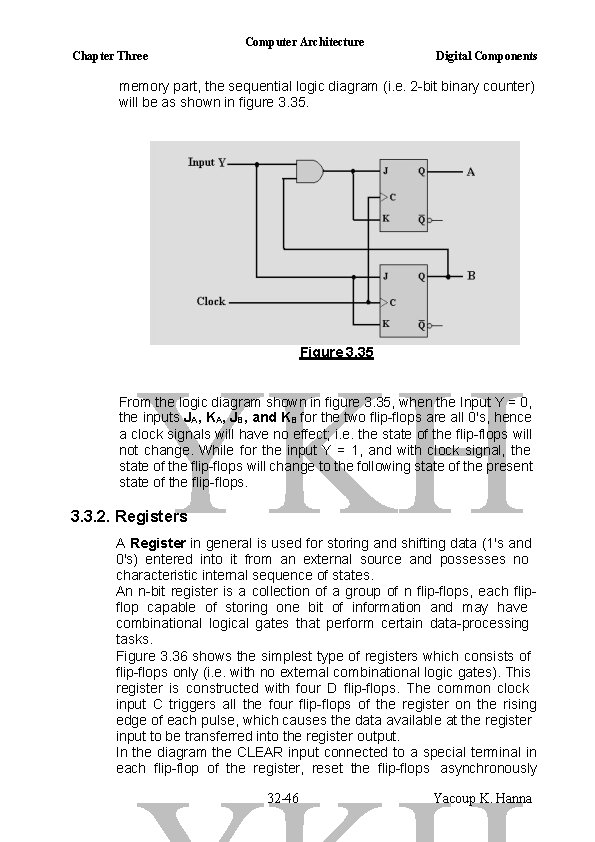
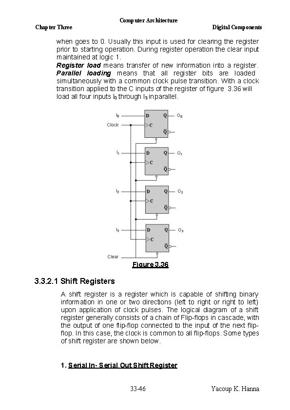
Computer Architecture Chapter Three Digital Components memory part, the sequential logic diagram (i. e. 2 -bit binary counter) will be as shown in figure 3. 35. Figure 3. 35 From the logic diagram shown in figure 3. 35, when the Input Y = 0, the inputs JA, KA, JB, and KB for the two flip-flops are all 0's, hence a clock signals will have no effect; i. e. the state of the flip-flops will not change. While for the input Y = 1, and with clock signal, the state of the flip-flops will change to the following state of the present state of the flip-flops. 3. 3. 2. Registers A Register in general is used for storing and shifting data (1's and 0's) entered into it from an external source and possesses no characteristic internal sequence of states. An n-bit register is a collection of a group of n flip-flops, each flipflop capable of storing one bit of information and may have combinational logical gates that perform certain data-processing tasks. Figure 3. 36 shows the simplest type of registers which consists of flip-flops only (i. e. with no external combinational logic gates). This register is constructed with four D flip-flops. The common clock input C triggers all the four flip-flops of the register on the rising edge of each pulse, which causes the data available at the register input to be transferred into the register output. In the diagram the CLEAR input connected to a special terminal in each flip-flop of the register, reset the flip-flops asynchronously 32 -46 Yacoup K. Hanna

Computer Architecture Chapter Three Digital Components when goes to 0. Usually this input is used for clearing the register prior to starting operation. During register operation the clear input maintained at logic 1. Register load means transfer of new information into a register. Parallel loading means that all register bits are loaded simultaneously with a common clock pulse transition. With a clock transition applied to the C inputs of the register of figure 3. 36 will load all four inputs I 0 through I 3 in parallel. Figure 3. 36 3. 3. 2. 1 Shift Registers A shift register is a register which is capable of shifting binary information in one or two directions (left to right or right to left) upon application of clock pulses. The logical diagram of a shift register generally consists of a chain of Flip-flops in cascade, with the output of one flip-flop connected to the input of the next flipflop. In this case, the clock is common to all flip-flops. Some types of shift register are shown below. 1. Serial In- Serial Out Shift Register 33 -46 Yacoup K. Hanna

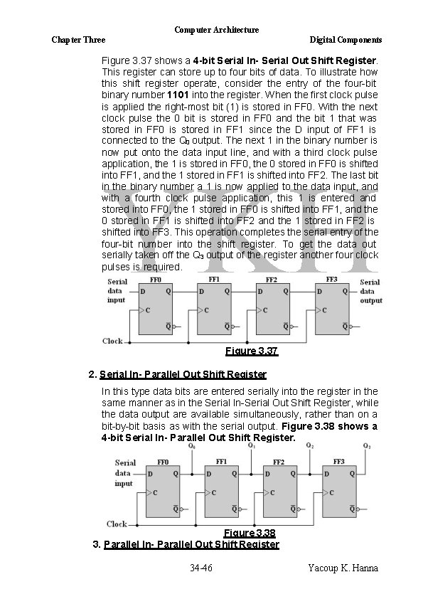
Computer Architecture Chapter Three Digital Components Figure 3. 37 shows a 4 -bit Serial In- Serial Out Shift Register. This register can store up to four bits of data. To illustrate how this shift register operate, consider the entry of the four-bit binary number 1101 into the register. When the first clock pulse is applied the right-most bit (1) is stored in FF 0. With the next clock pulse the 0 bit is stored in FF 0 and the bit 1 that was stored in FF 0 is stored in FF 1 since the D input of FF 1 is connected to the Q 0 output. The next 1 in the binary number is now put onto the data input line, and with a third clock pulse application, the 1 is stored in FF 0, the 0 stored in FF 0 is shifted into FF 1, and the 1 stored in FF 1 is shifted into FF 2. The last bit in the binary number a 1 is now applied to the data input, and with a fourth clock pulse application, this 1 is entered and stored into FF 0, the 1 stored in FF 0 is shifted into FF 1, and the 0 stored in FF 1 is shifted into FF 2 and the 1 stored in FF 2 is shifted into FF 3. This operation completes the serial entry of the four-bit number into the shift register. To get the data out serially taken off the Q 3 output of the register another four clock pulses is required. Figure 3. 37 2. Serial In- Parallel Out Shift Register In this type data bits are entered serially into the register in the same manner as in the Serial In-Serial Out Shift Register, while the data output are available simultaneously, rather than on a bit-by-bit basis as with the serial output. Figure 3. 38 shows a 4 -bit Serial In- Parallel Out Shift Register. Figure 3. 38 3. Parallel In- Parallel Out Shift Register 34 -46 Yacoup K. Hanna

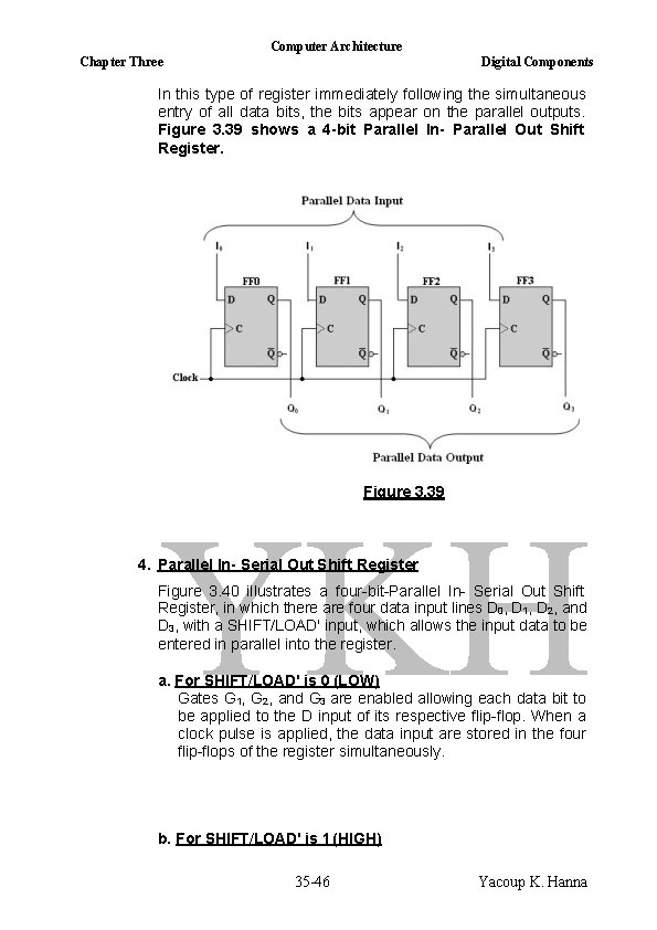
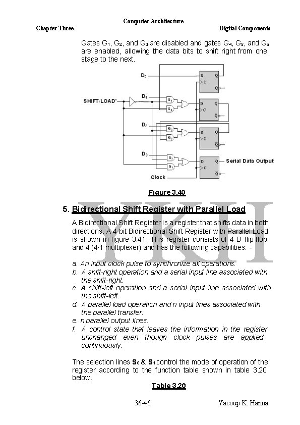
Computer Architecture Chapter Three Digital Components In this type of register immediately following the simultaneous entry of all data bits, the bits appear on the parallel outputs. Figure 3. 39 shows a 4 -bit Parallel In- Parallel Out Shift Register. Figure 3. 39 4. Parallel In- Serial Out Shift Register Figure 3. 40 illustrates a four-bit-Parallel In- Serial Out Shift Register, in which there are four data input lines D 0, D 1, D 2, and D 3, with a SHIFT/LOAD' input, which allows the input data to be entered in parallel into the register. a. For SHIFT/LOAD' is 0 (LOW) Gates G 1, G 2, and G 3 are enabled allowing each data bit to be applied to the D input of its respective flip-flop. When a clock pulse is applied, the data input are stored in the four flip-flops of the register simultaneously. b. For SHIFT/LOAD' is 1 (HIGH) 35 -46 Yacoup K. Hanna

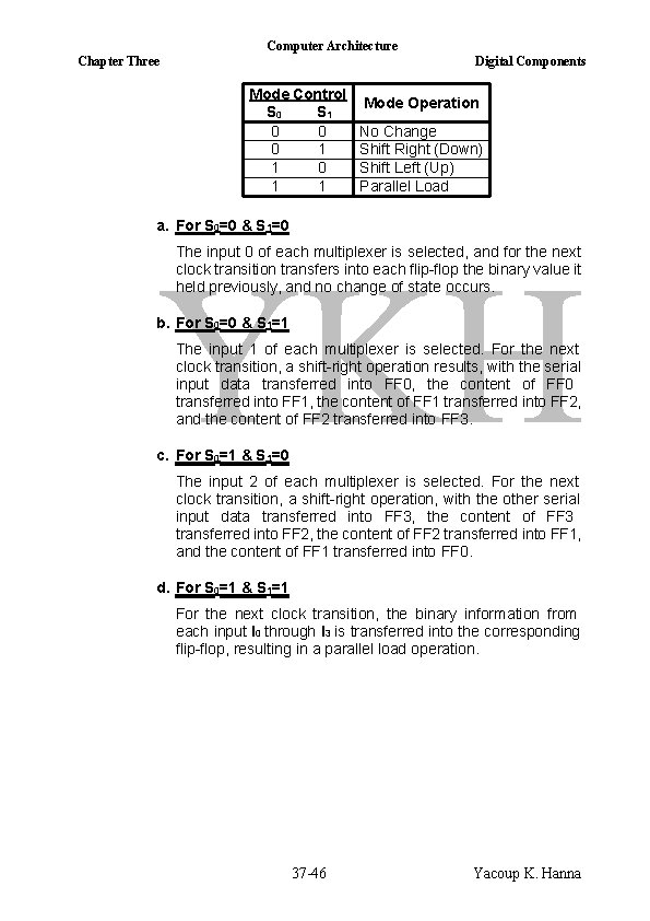
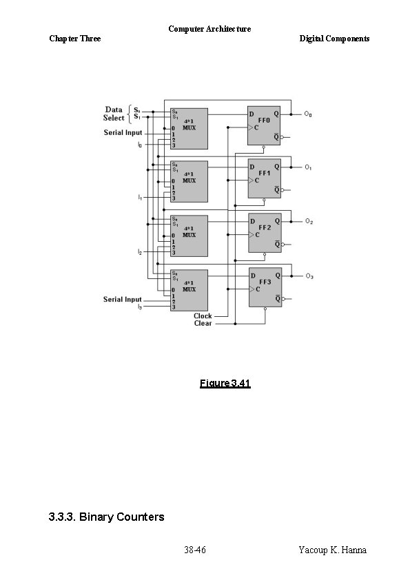
Computer Architecture Chapter Three Digital Components Gates G 1, G 2, and G 3 are disabled and gates G 4, G 5, and G 6 are enabled, allowing the data bits to shift right from one stage to the next. Figure 3. 40 5. Bidirectional Shift Register with Parallel Load A Bidirectional Shift Register is a register that shifts data in both directions. A 4 -bit Bidirectional Shift Register with Parallel Load is shown in figure 3. 41. This register consists of 4 D flip-flop and 4 (4*1 multiplexer) and has the following capabilities: - a. An input clock pulse to synchronize all operations. b. A shift-right operation and a serial input line associated with the shift-right. c. A shift-left operation and a serial input line associated with the shift-left. d. A parallel load operation and n input lines associated with the parallel transfer. e. n parallel output lines. f. A control state that leaves the information in the register unchanged even though clock pulses are applied continuously. The selection lines S 0 & S 1 control the mode of operation of the register according to the function table shown in table 3. 20 below. Table 3. 20 36 -46 Yacoup K. Hanna

Computer Architecture Chapter Three Digital Components Mode Control S 0 S 1 0 0 0 1 1 Mode Operation No Change Shift Right (Down) Shift Left (Up) Parallel Load a. For S 0=0 & S 1=0 The input 0 of each multiplexer is selected, and for the next clock transition transfers into each flip-flop the binary value it held previously, and no change of state occurs. b. For S 0=0 & S 1=1 The input 1 of each multiplexer is selected. For the next clock transition, a shift-right operation results, with the serial input data transferred into FF 0, the content of FF 0 transferred into FF 1, the content of FF 1 transferred into FF 2, and the content of FF 2 transferred into FF 3. c. For S 0=1 & S 1=0 The input 2 of each multiplexer is selected. For the next clock transition, a shift-right operation, with the other serial input data transferred into FF 3, the content of FF 3 transferred into FF 2, the content of FF 2 transferred into FF 1, and the content of FF 1 transferred into FF 0. d. For S 0=1 & S 1=1 For the next clock transition, the binary information from each input I 0 through I 3 is transferred into the corresponding flip-flop, resulting in a parallel load operation. 37 -46 Yacoup K. Hanna

Computer Architecture Chapter Three Digital Components Figure 3. 41 3. 3. 3. Binary Counters 38 -46 Yacoup K. Hanna

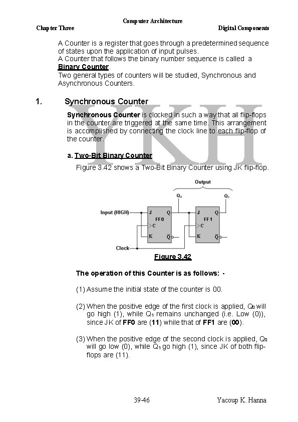
Computer Architecture Chapter Three Digital Components A Counter is a register that goes through a predetermined sequence of states upon the application of input pulses. A Counter that follows the binary number sequence is called a Binary Counter. Two general types of counters will be studied, Synchronous and Asynchronous Counters. 1. Synchronous Counter is clocked in such a way that all flip-flops in the counter are triggered at the same time. This arrangement is accomplished by connecting the clock line to each flip-flop of the counter. a. Two-Bit Binary Counter Figure 3. 42 shows a Two-Bit Binary Counter using JK flip-flop. Figure 3. 42 The operation of this Counter is as follows: - (1) Assume the initial state of the counter is 00. (2) When the positive edge of the first clock is applied, Q 0 will go high (1), while Q 1 remains unchanged (i. e. Low (0)), since JK of FF 0 are (11) while that of FF 1 are (00). (3) When the positive edge of the second clock is applied, Q 0 will go low (0), while Q 1 go high (1), since JK of both flipflops are (11). 39 -46 Yacoup K. Hanna

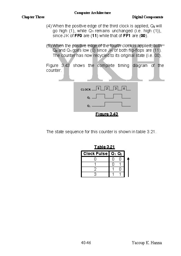
Computer Architecture Chapter Three Digital Components (4) When the positive edge of the third clock is applied, Q 0 will go high (1), while Q 1 remains unchanged (i. e. high (1)), since JK of FF 0 are (11) while that of FF 1 are (00). (5) When the positive edge of the fourth clock is applied, both Q 0 and Q 1 goes low (0) since JK of both flip-flops are (11). The counter has now recycled to its original state (i. e. 00). Figure 3. 43 shows the complete timing diagram of the counter. Figure 3. 43 The state sequence for this counter is shown in table 3. 21. Table 3. 21 Clock Pulse Q 1 0 0 1 0 2 1 3 1 40 -46 Q 0 0 1 Yacoup K. Hanna

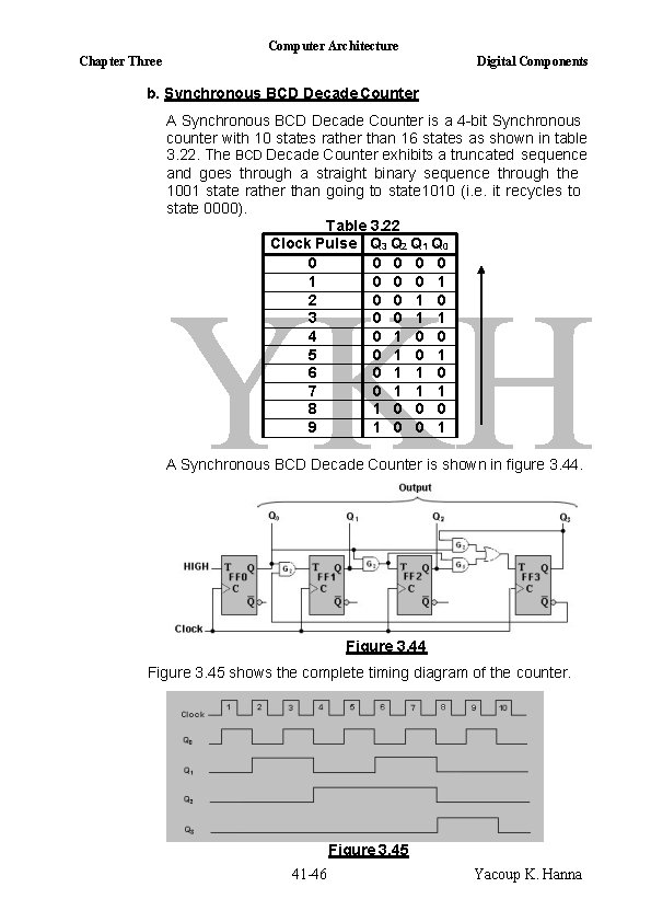
Computer Architecture Chapter Three Digital Components b. Synchronous BCD Decade Counter A Synchronous BCD Decade Counter is a 4 -bit Synchronous counter with 10 states rather than 16 states as shown in table 3. 22. The BCD Decade Counter exhibits a truncated sequence and goes through a straight binary sequence through the 1001 state rather than going to state 1010 (i. e. it recycles to state 0000). Table 3. 22 Clock Pulse Q 3 Q 2 Q 1 Q 0 0 0 1 2 0 0 1 0 3 0 0 1 1 4 0 1 0 0 5 0 1 6 0 1 1 0 7 0 1 1 1 8 1 0 0 0 9 1 0 0 1 A Synchronous BCD Decade Counter is shown in figure 3. 44. Figure 3. 44 Figure 3. 45 shows the complete timing diagram of the counter. Figure 3. 45 41 -46 Yacoup K. Hanna

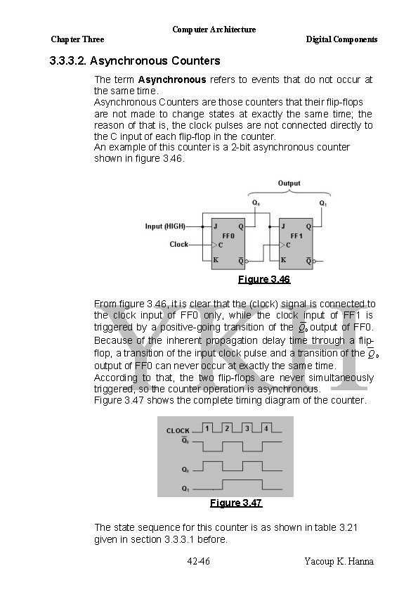
Computer Architecture Chapter Three Digital Components 3. 3. 3. 2. Asynchronous Counters The term Asynchronous refers to events that do not occur at the same time. Asynchronous Counters are those counters that their flip-flops are not made to change states at exactly the same time; the reason of that is, the clock pulses are not connected directly to the C input of each flip-flop in the counter. An example of this counter is a 2 -bit asynchronous counter shown in figure 3. 46. Figure 3. 46 From figure 3. 46, it is clear that the (clock) signal is connected to the clock input of FF 0 only, while the clock input of FF 1 is triggered by a positive-going transition of the Q 0 output of FF 0. Because of the inherent propagation delay time through a flipflop, a transition of the input clock pulse and a transition of the Q 0 output of FF 0 can never occur at exactly the same time. According to that, the two flip-flops are never simultaneously triggered, so the counter operation is asynchronous. Figure 3. 47 shows the complete timing diagram of the counter. Figure 3. 47 The state sequence for this counter is as shown in table 3. 21 given in section 3. 3. 3. 1 before. 42 -46 Yacoup K. Hanna

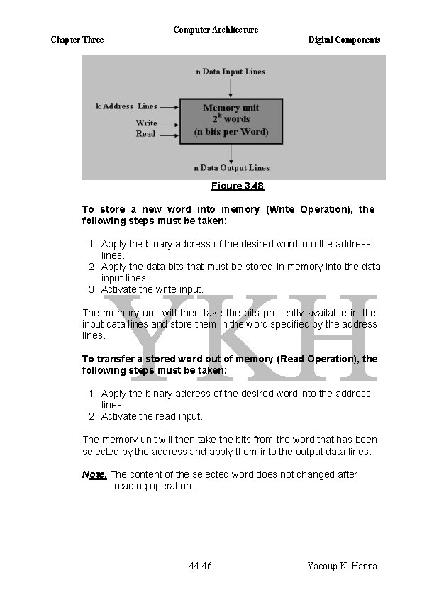
Computer Architecture Chapter Three 4. Digital Components Memory Unit A collection of storage cells together with associated control circuits needed to transfer information in & out of storage is called Memory Unit. The memory stores binary information in groups of bits called Words. A group of 1's and 0's usually a multiple of 8 -bits (16 -bits, 32 -bits, 64 bits …etc) is a Memory Word. The memory word may represent a number, an instruction code, one or more alphanumeric characters, or any other binary-coded information. A group of 8 -bits is called a Byte. Commercially, the capacity of memories in a computer is usually stated as the total number of bytes that can be stored. Each word in memory has an address, starting from (0) up to (2 k – 1) where k is the number of address lines. The selection of a specified word in the memory is done by applying the n-bit binary address to the address lines. Computer memories may range from 1024 words, requiring an address of 10 bits, to 232 words, requiring 32 address bits. A decoder inside the memory accepts the address and opens the path needed to select the required word. Generally two major types of memories are used in computer systems: a. Random Access Memory (RAM). b. Read-Only Memory (ROM). 3. 4. 1. Random Access Memory (RAM) In this type of memories, memory cells can be accessed for information transfer purposes from any desired random location. That is, the time needed for locating a word in memory is the same no matter where the cells are located physically in memory. Communication between a memory and its environment is achieved through data input & output lines, address lines, and control lines that specify the direction of transfer. Figure 3. 48 shows a block diagram of a RAM unit. In the diagram, the n data input lines provide the information to be stored in memory, and the n data output lines supply the information coming out of memory. The k address lines provide the address of the word required among the 2 k available words inside the memory. The two control inputs named Read & Write specify the direction of transfer desired. 43 -46 Yacoup K. Hanna

Computer Architecture Chapter Three Digital Components Figure 3. 48 To store a new word into memory (Write Operation), the following steps must be taken: 1. Apply the binary address of the desired word into the address lines. 2. Apply the data bits that must be stored in memory into the data input lines. 3. Activate the write input. The memory unit will then take the bits presently available in the input data lines and store them in the word specified by the address lines. To transfer a stored word out of memory (Read Operation), the following steps must be taken: 1. Apply the binary address of the desired word into the address lines. 2. Activate the read input. The memory unit will then take the bits from the word that has been selected by the address and apply them into the output data lines. Note. The content of the selected word does not changed after reading operation. 44 -46 Yacoup K. Hanna

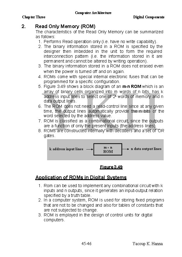
Computer Architecture Chapter Three 2. Digital Components Read Only Memory (ROM) The characteristics of the Read Only Memory can be summarized as follows: 1. Performs Read operation only (i. e. have no write capability). 2. The binary information stored in a ROM is specified by the designer then imbedded in the unit to form the required interconnection pattern (i. e. the information stored in it are permanent and cannot be altered by writing operation). 3. The binary information stored in a ROM does not erased even when the power is turned off and on again. 4. ROMs come with special internal electronic fuses that can be programmed for a specific configuration. 5. Figure 3. 49 shows a block diagram of an m*n ROM which is an array of binary cells organized into m words of n bits, has k address input lines to select one of 2 k words of memory and n data output lines. 6. The ROM does not need a read-control line since at any given time, the output lines automatically provide the n bits of the word selected by the address value. 7. ROM is classified as a combinational circuit, since the outputs are a function of only the present inputs (the address lines). 8. ROMs are constructed internally with decoders and a set of OR gates. Figure 3. 49 Application of ROMs in Digital Systems 1. Rom can be used to implement any combinational circuit with k inputs and n outputs, since it generates an input-output relation specified by a truth table. 2. In a computer system, ROM is used for storing fixed programs that are not to be changed and also for tables of constants that are not subjected to change. 3. ROM is employed in the design of control units for digital computers. 45 -46 Yacoup K. Hanna

Computer Architecture Chapter Three Digital Components Types of ROMs The required paths in a ROM may be programmed in three different ways: - 1. Mask Programming This is done by the semiconductor company during the last fabrication process of the unit. The procedure for fabricating a ROM requires: a. The customer fills out the truth table according to his or her requirement and submitted in a special form provided by the manufacturer. b. The manufacturer makes the corresponding mask for the paths to produce the 1's and 0's according to the customer's truth table. 2. Programmable Read-Only Memory (PROM) PROM units contain from the manufacturer all fuses intact, giving all 1's in the bits of the stored words. PROM is programmed by the designer according to his or her requirement using a special instrument available commercially to facilitate this procedure called PROM Programmers. Programming process takes place by that the fuses in the PROM are blown by application of current pulses through the output terminals for each address. A blown fuse defines a binary 0 state, and an intact fuse gives a binary 1 state. 3. Erasable PROM (EPROM) The EPROM can be restructured to the initial value even though its fuses have been blown previously. To erase the EPROM, it is placed under a special ultraviolet light for a given period of time, in which the shortwave radiation discharges the internal gates that serve as fuses. After this erasing process, the EPROM returns to its initial state and can be reprogrammed to a new set of words. 46 -46 Yacoup K. Hanna