Computer Architecture Chapter Five Register Transfer and Microoperations
- Slides: 10

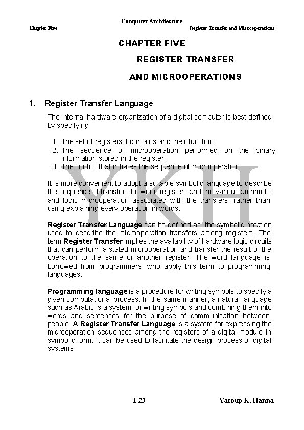
Computer Architecture Chapter Five Register Transfer and Microoperations CHAPTER FIVE REGISTER TRANSFER AND MICROOPERATIONS 1. Register Transfer Language The internal hardware organization of a digital computer is best defined by specifying: 1. The set of registers it contains and their function. 2. The sequence of microoperation performed on the binary information stored in the register. 3. The control that initiates the sequence of microoperation. It is more convenient to adopt a suitable symbolic language to describe the sequence of transfers between registers and the various arithmetic and logic microoperation associated with the transfers, rather than using explaining every operation in words. Register Transfer Language can be defined as, the symbolic notation used to describe the microoperation transfers among registers. The term Register Transfer implies the availability of hardware logic circuits that can perform a stated microoperation and transfer the result of the operation to the same or another register. The word language is borrowed from programmers, who apply this term to programming languages. Programming language is a procedure for writing symbols to specify a given computational process. In the same manner, a natural language such as Arabic is a system for writing symbols and combining them into words and sentences for the purpose of communication between people. A Register Transfer Language is a system for expressing the microoperation sequences among the registers of a digital module in symbolic form. It can be used to facilitate the design process of digital systems. 1 -23 Yacoup K. Hanna

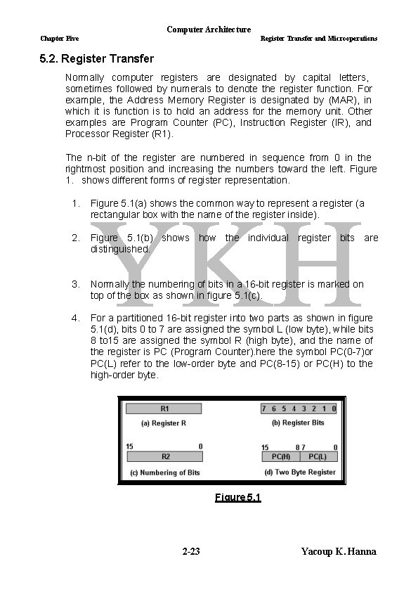
Computer Architecture Chapter Five Register Transfer and Microoperations 5. 2. Register Transfer Normally computer registers are designated by capital letters, sometimes followed by numerals to denote the register function. For example, the Address Memory Register is designated by (MAR), in which it is function is to hold an address for the memory unit. Other examples are Program Counter (PC), Instruction Register (IR), and Processor Register (R 1). The n-bit of the register are numbered in sequence from 0 in the rightmost position and increasing the numbers toward the left. Figure 1. shows different forms of register representation. 1. Figure 5. 1(a) shows the common way to represent a register (a rectangular box with the name of the register inside). 2. Figure 5. 1(b) shows how the individual register bits are distinguished. 3. Normally the numbering of bits in a 16 -bit register is marked on top of the box as shown in figure 5. 1(c). 4. For a partitioned 16 -bit register into two parts as shown in figure 5. 1(d), bits 0 to 7 are assigned the symbol L (low byte), while bits 8 to 15 are assigned the symbol R (high byte), and the name of the register is PC (Program Counter). here the symbol PC(0 -7)or PC(L) refer to the low-order byte and PC(8 -15) or PC(H) to the high-order byte. Figure 5. 1 2 -23 Yacoup K. Hanna

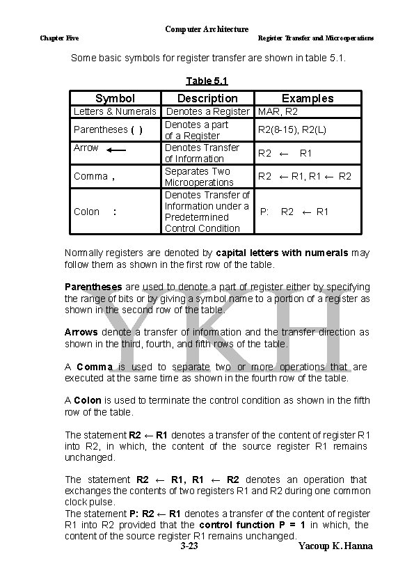
Computer Architecture Chapter Five Register Transfer and Microoperations Some basic symbols for register transfer are shown in table 5. 1. Table 5. 1 Symbol Description Letters & Numerals Denotes a Register Denotes a part Parentheses ( ) of a Register Arrow Denotes Transfer of Information Separates Two Comma , Microoperations Denotes Transfer of Information under a Colon : Predetermined Control Condition Examples MAR, R 2(8 -15), R 2(L) R 2 ← R 1, R 1 ← R 2 P: R 2 ← R 1 Normally registers are denoted by capital letters with numerals may follow them as shown in the first row of the table. Parentheses are used to denote a part of register either by specifying the range of bits or by giving a symbol name to a portion of a register as shown in the second row of the table. Arrows denote a transfer of information and the transfer direction as shown in the third, fourth, and fifth rows of the table. A Comma is used to separate two or more operations that are executed at the same time as shown in the fourth row of the table. A Colon is used to terminate the control condition as shown in the fifth row of the table. The statement R 2 ← R 1 denotes a transfer of the content of register R 1 into R 2, in which, the content of the source register R 1 remains unchanged. The statement R 2 ← R 1, R 1 ← R 2 denotes an operation that exchanges the contents of two registers R 1 and R 2 during one common clock pulse. The statement P: R 2 ← R 1 denotes a transfer of the content of register R 1 into R 2 provided that the control function P = 1 in which, the content of the source register R 1 remains unchanged. 3 -23 Yacoup K. Hanna

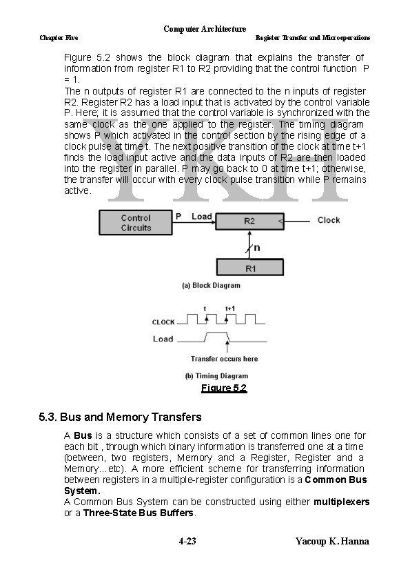
Computer Architecture Chapter Five Register Transfer and Microoperations Figure 5. 2 shows the block diagram that explains the transfer of information from register R 1 to R 2 providing that the control function P = 1. The n outputs of register R 1 are connected to the n inputs of register R 2. Register R 2 has a load input that is activated by the control variable P. Here; it is assumed that the control variable is synchronized with the same clock as the one applied to the register. The timing diagram shows P which activated in the control section by the rising edge of a clock pulse at time t. The next positive transition of the clock at time t+1 finds the load input active and the data inputs of R 2 are then loaded into the register in parallel. P may go back to 0 at time t+1; otherwise, the transfer will occur with every clock pulse transition while P remains active. Figure 5. 2 5. 3. Bus and Memory Transfers A Bus is a structure which consists of a set of common lines one for each bit , through which binary information is transferred one at a time (between, two registers, Memory and a Register, Register and a Memory…etc). A more efficient scheme for transferring information between registers in a multiple-register configuration is a Common Bus System. A Common Bus System can be constructed using either multiplexers or a Three-State Bus Buffers. 4 -23 Yacoup K. Hanna

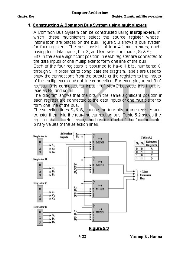
Computer Architecture Chapter Five Register Transfer and Microoperations 1. Constructing A Common Bus System using multiplexers A Common Bus System can be constructed using multiplexers, in which, these multiplexers select the source register whose information are placed on the bus. Figure 5. 3 shows a bus system for four registers. The bus consists of four 4*1 multiplexers, each having four data inputs, 0 to 3, and two selection inputs, S 1 & S 0. Bits in the same significant position in each register are connected to the data inputs of one multiplexer to form one line of the bus. Each of the four registers is assumed to have 4 bits, numbered 0 through 3. In order not to complicate the diagram, labels are used to show the connections from the outputs of the registers to the inputs of the multiplexers and not line connection. For example, output 3 of register B is connected to input 1 of MUX 3 because this input is labeled B 3, and so on. The diagram shows that the bits in the same significant position in each register are connected to the data inputs of one multiplexer to form one line of the bus. The selection lines S 1 & S 0 choose the four bits of one register and transfer them into the four-line connection bus. Table 5. 2 shows the register that is selected by the bus for each of the four possible binary values of the selection lines. Figure 5. 3 5 -23 Yacoup K. Hanna

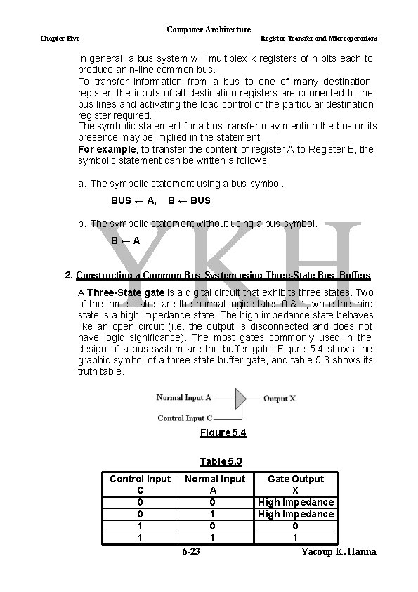
Computer Architecture Chapter Five Register Transfer and Microoperations In general, a bus system will multiplex k registers of n bits each to produce an n-line common bus. To transfer information from a bus to one of many destination register, the inputs of all destination registers are connected to the bus lines and activating the load control of the particular destination register required. The symbolic statement for a bus transfer may mention the bus or its presence may be implied in the statement. For example, to transfer the content of register A to Register B, the symbolic statement can be written a follows: a. The symbolic statement using a bus symbol. BUS ← A, B ← BUS b. The symbolic statement without using a bus symbol. B←A 2. Constructing a Common Bus System using Three-State Bus Buffers A Three-State gate is a digital circuit that exhibits three states. Two of the three states are the normal logic states 0 & 1, while third state is a high-impedance state. The high-impedance state behaves like an open circuit (i. e. the output is disconnected and does not have logic significance). The most gates commonly used in the design of a bus system are the buffer gate. Figure 5. 4 shows the graphic symbol of a three-state buffer gate, and table 5. 3 shows its truth table. Figure 5. 4 Table 5. 3 Control Input C 0 0 1 1 Normal Input A 0 1 6 -23 Gate Output X High Impedance 0 1 Yacoup K. Hanna

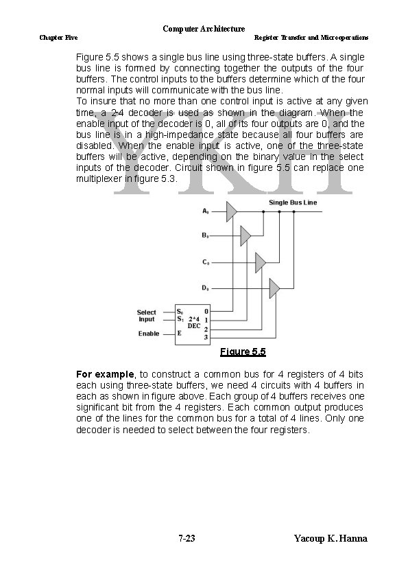
Computer Architecture Chapter Five Register Transfer and Microoperations Figure 5. 5 shows a single bus line using three-state buffers. A single bus line is formed by connecting together the outputs of the four buffers. The control inputs to the buffers determine which of the four normal inputs will communicate with the bus line. To insure that no more than one control input is active at any given time, a 2*4 decoder is used as shown in the diagram. When the enable input of the decoder is 0, all of its four outputs are 0, and the bus line is in a high-impedance state because all four buffers are disabled. When the enable input is active, one of the three-state buffers will be active, depending on the binary value in the select inputs of the decoder. Circuit shown in figure 5. 5 can replace one multiplexer in figure 5. 3. Figure 5. 5 For example, to construct a common bus for 4 registers of 4 bits each using three-state buffers, we need 4 circuits with 4 buffers in each as shown in figure above. Each group of 4 buffers receives one significant bit from the 4 registers. Each common output produces one of the lines for the common bus for a total of 4 lines. Only one decoder is needed to select between the four registers. 7 -23 Yacoup K. Hanna

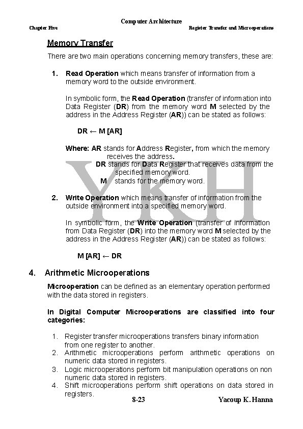
Computer Architecture Chapter Five Register Transfer and Microoperations Memory Transfer There are two main operations concerning memory transfers, these are: 1. Read Operation which means transfer of information from a memory word to the outside environment. In symbolic form, the Read Operation (transfer of information into Data Register (DR) from the memory word M selected by the address in the Address Register (AR)) can be stated as follows: DR ← M [AR] Where: AR stands for Address Register, from which the memory receives the address. DR stands for Data Register that receives data from the specified memory word. M stands for the memory word. 2. Write Operation which means transfer of information from the outside environment into a specified memory word. In symbolic form, the Write Operation (transfer of information from Data Register (DR) into the memory word M selected by the address in the Address Register (AR)) can be stated as follows: M [AR] ← DR 4. Arithmetic Microoperations Microoperation can be defined as an elementary operation performed with the data stored in registers. In Digital Computer Microoperations are classified into four categories: 1. Register transfer microoperations transfers binary information from one register to another. 2. Arithmetic microoperations perform arithmetic operations on numeric data stored in registers. 3. Logic microoperations perform bit manipulation operations on numeric data stored in registers. 4. Shift microoperations perform shift operations on data stored in registers. 8 -23 Yacoup K. Hanna

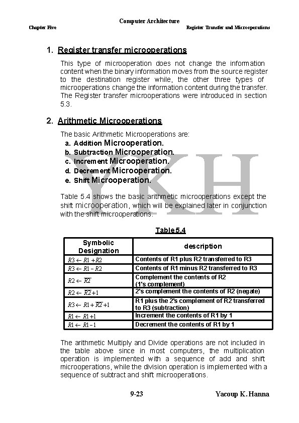
Computer Architecture Chapter Five Register Transfer and Microoperations 1. Register transfer microoperations This type of microoperation does not change the information content when the binary information moves from the source register to the destination register while, the other three types of microoperations change the information content during the transfer. The Register transfer microoperations were introduced in section 5. 3. 2. Arithmetic Microoperations The basic Arithmetic Microoperations are: a. Addition Microoperation. b. Subtraction Microoperation. c. Increment Microoperation. d. Decrement Microoperation. e. Shift Microoperation. Table 5. 4 shows the basic arithmetic microoperations except the shift microoperation, which will be explained later in conjunction with the shift microoperations. Table 5. 4 Symbolic Designation R 3 R 1 R 2 R 2 1 R 3 R 1 R 2 1 R 1 1 description Contents of R 1 plus R 2 transferred to R 3 Contents of R 1 minus R 2 transferred to R 3 Complement the contents of R 2 (1's complement) 2's complement the contents of R 2 (negate) R 1 plus the 2's complement of R 2 transferred to R 3 (subtraction) Increment the contents of R 1 by 1 Decrement the contents of R 1 by 1 The arithmetic Multiply and Divide operations are not included in the table above since in most computers, the multiplication operation is implemented with a sequence of add and shift microoperations, while the division operation is implemented with a sequence of subtract and shift microoperations. 9 -23 Yacoup K. Hanna

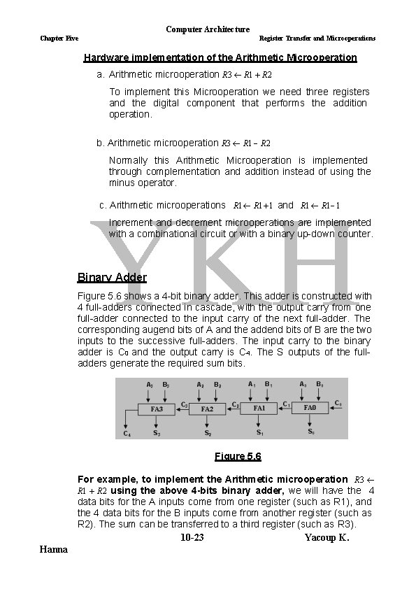
Computer Architecture Chapter Five Register Transfer and Microoperations Hardware implementation of the Arithmetic Microoperation a. Arithmetic microoperation R 3 R 1 R 2 To implement this Microoperation we need three registers and the digital component that performs the addition operation. b. Arithmetic microoperation R 3 R 1 R 2 Normally this Arithmetic Microoperation is implemented through complementation and addition instead of using the minus operator. c. Arithmetic microoperations R 1 1 and R 1 1 Increment and decrement microoperations are implemented with a combinational circuit or with a binary up-down counter. Binary Adder Figure 5. 6 shows a 4 -bit binary adder. This adder is constructed with 4 full-adders connected in cascade, with the output carry from one full-adder connected to the input carry of the next full-adder. The corresponding augend bits of A and the addend bits of B are the two inputs to the successive full-adders. The input carry to the binary adder is C 0 and the output carry is C 4. The S outputs of the fulladders generate the required sum bits. Figure 5. 6 For example, to implement the Arithmetic microoperation R 3 R 1 R 2 using the above 4 -bits binary adder, we will have the 4 data bits for the A inputs come from one register (such as R 1), and the 4 data bits for the B inputs come from another register (such as R 2). The sum can be transferred to a third register (such as R 3). 10 -23 Yacoup K. Hanna