Computer Aided Design Course 4 AC Analyses The


/V(Vin))")


 shows: Av=3. 99 d. B şi B-3")


- Slides: 24
Computer Aided Design Course 4
AC Analyses The frequency response analysis calculates the small-signal response of the circuit, linearized around the bias point, to a combination of inputs. For nonlinear devices, such as voltage-controlled or currentcontrolled switches, a linearisation around their bias point value is carried out, and then follows a linear (small-signal) analysis. In the case of semiconductor devices manifesting a high degree of nonlinearity, for instance, a bipolar transistor in common-emitter mode, the device would be automatically replaced by a constant transconductance (collector current proportional to base-emitter voltage), plus a number of constant impedances. Generally speaking, for each device exhibiting nonlinearity PSpice A/D determines a set of partial derivatives at the bias point, and these are then used in small-signal analysis.
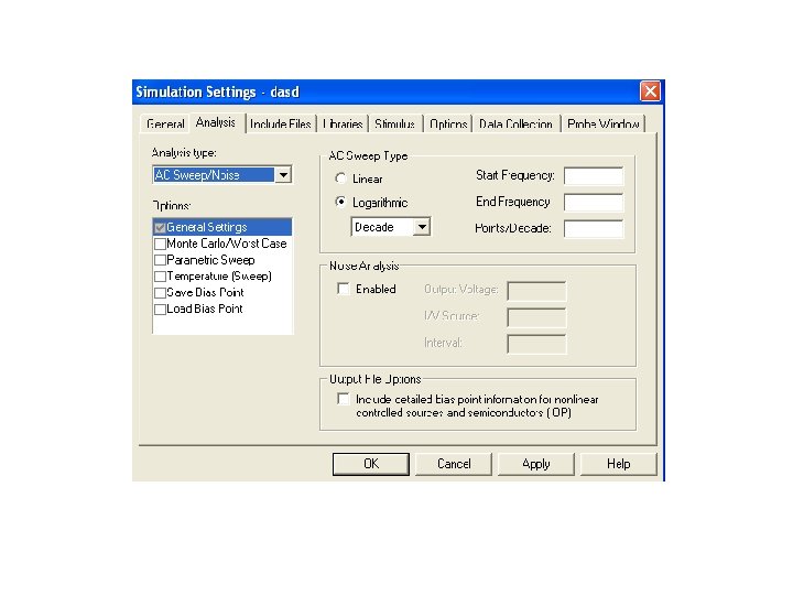
In order to organize set up and run AC Analyses, for example, you would go through the following steps: • Applying an appropriate AC stimulus • Setting up AC Sweep type • Setting up Noise analysis
1. AC stimulus In order to perform an AC analysis, first you will have to correspondingly prepare your design circuit in Schematics. This means that you will have to introduce, i. e. to place and connect, one or more independent voltage or/and current sources (i. e. input signal sources). After introducing the desired source or sources, it is very important that you define correctly its or their names and attributes. Note: The best way to use AC sweep analysis is to set the source magnitude to one. This way, the measured output equals the gain, relative to the input source, at that output.
2. AC Sweep AC sweep is a frequency response analysis. PSpice A/D calculates the small-signal response of the circuit, linearized around the bias point, to a combination of inputs. All admitances are complex numbers, depending by the frequency: Y=G+j C+1/j L where: =2 f. The variables are complex numbers:
The output variables use the following suffixes: None- magnitude M – absolute value DB – (logarithmic) absolute value in decibels P - phase G – group delay (-d. PHASE/d. FREQUENCY) R – real part I – imaginary part
Ca n be ploted the following characteristics: Bode diagrams: - magnitude vs. frequency DB(V(out)/V(Vin)) =VDB(out)-VDB(Vin) = 20 log 10(V(out)/V(Vin)) - phase vs, frequency VP(out)-VP(Vin) for logarithmic frequency sweept: (DEC) or (OCT).
Input impedance: Output impedance: Group delay is time between groups of pulses.
Minimum Circuit Design Requirements: Place and connect a voltage or current source with an AC input signal. Here we will consider that an AC Stimulus (voltage or current source with an AC input signal) is placed, connected and set. Minimum Program Setup Requirements: To complete the definition of the independent input sources you will have to set up the range and manner of frequency variation by using corresponding dialog boxes:
In the Start Freq and End Freq text boxes, enter the starting and ending frequencies, respectively, for the sweep.
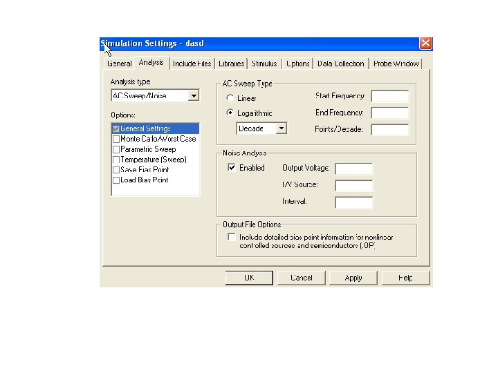
3. Noise Analysis When running a noise analysis, PSpice A/D calculates and reports the following for each frequency specified for the AC sweep analysis: • device noise, which is the noise contribution propagated to the specified output net from every resistor and semiconductor device in the circuit; for semiconductor devices, the device noise is also broken down into constituent noise contributions where applicable • total output and equivalent input noise
Resistors: • Thermal noise Semiconductor devices: • Thermal noise continuous noise • Shot noise • Flicker noise • Burst noise frequency noise
The total output noise is sum of root mean square values of each noise source. The root mean square value of noise current through resistors is: The noise sources are characterized by power spectral density: or
Using the calculated output total noise can be determined the signal/noise ratio:
Minimum Circuit Design Requirements: Place and connect a voltage or current source with an AC input signal. Here we will consider that an AC Stimulus (voltage or current source with an AC input signal) is placed, connected and set.
Minimum Program Setup Requirements: Noise in circuits is functionally dependent on the bias point DC value as well as on signal frequency. Therefore, it is necessary to carry out its calculation as a part of the AC analysis. Enter the noise analysis parameters as follows:
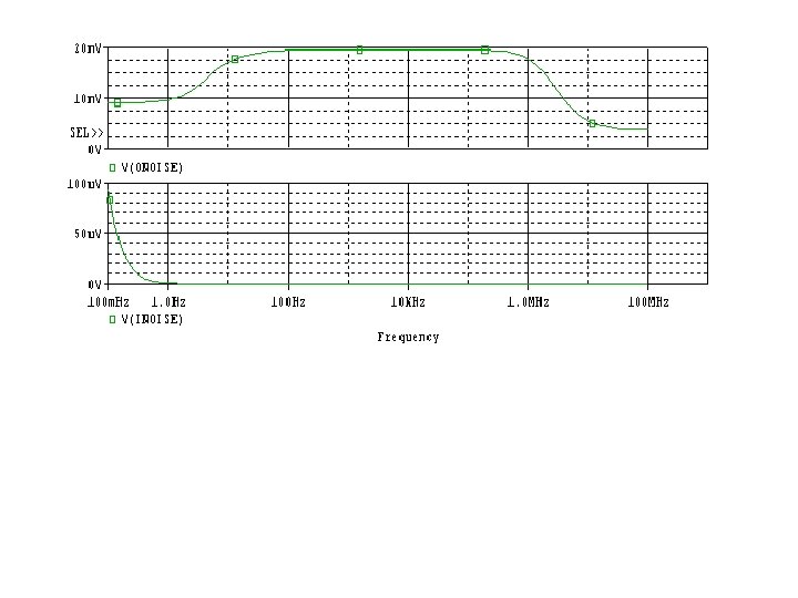
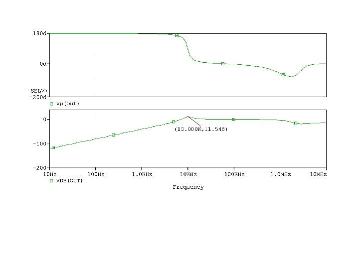
Example 1: Consider the CE-CC BJT amplifier. Determine the frequency response: the midband voltage gain and the 3 d. B frequencies, B-3 d. B; the output noise at out 2 and input noise at Vin.
Frequency response ( magnitude and phase characteristics) shows: Av=3. 99 d. B şi B-3 d. B is between 33. 8 Hz and 2. 2 MEGHz.
NOISE ANALYSIS TEMPERATURE = 27. 000 DEG C ************************************** FREQUENCY = 1. 000 E+04 HZ **** TRANSISTOR SQUARED NOISE VOLTAGES (SQ V/HZ) Q_Q 2 Q_Q 1 RB 1. 539 E-19 4. 155 E-19 RC 1. 042 E-24 2. 457 E-26 RE 0. 000 E+00 IBSN 1. 097 E-16 6. 750 E-17 IC 1. 098 E-18 1. 564 E-18 IBFN 0. 000 E+00 TOTAL 1. 110 E-16 6. 948 E-17 **** RESISTOR SQUARED NOISE VOLTAGES (SQ V/HZ) R_R 5 R_R 4 R_R 3 R_R 2 R_R 1 R_R 6 R_R 7 TOTAL 1. 052 E-22 1. 248 E-16 7. 681 E-17 9. 168 E-22 1. 681 E-20 2. 105 E-22 7. 238 E-21 **** TOTAL OUTPUT NOISE VOLTAGE = 3. 821 E-16 SQ V/HZ = 1. 955 E-08 V/RT HZ TRANSFER FUNCTION VALUE: V(OUT 2)/V_Vin = 1. 583 E+00 EQUIVALENT INPUT NOISE AT V_Vin = 1. 235 E-08 V/RT HZ
Example 3: Consider a second-order high-pass active filter with f 0=10 k. Hz and Q=4. Determine the frequency response and 3 d. B frequency.