Compute DRAM InMemory Compute using OfftheShelf DRAMs IEEEACM
- Slides: 33

Compute. DRAM: In-Memory Compute using Off-the-Shelf DRAMs IEEE/ACM International Symposium on Microarchitecture (MICRO -52) 12/2019 Fei Gao Princeton University Georgios Tziantzioulis Princeton University David Wentzlaff Princeton University Seminar in Computer Architecture Today’s Presenter: Patrick Eppensteiner Compute. DRAM SEMINAR IN COMPUTER ARCHITECTURE 1

Executive Summary Problem: Memory Wall ◦ Moving data from and to memory incurs long access latency ◦ Existing solutions are not feasible (for DRAM manufacturers) Goal: Proof of concept that in-memory computation is possible with unmodified DRAM modules Compute. DRAM ◦ In-memory computation using minimal modifications ◦ Off-the-shelf, unmodified, commercial DRAM ◦ Row Copy, AND and OR: logical completeness by saving inverse values as well ◦ Arbitrary computations made possible using a modified memory controller Results ◦ In-memory computation possible with unmodified DRAM modules ◦ Financially feasible way for DRAM manufacturers to support in-memory compute Compute. DRAM SEMINAR IN COMPUTER ARCHITECTURE 2

Problem & Goal Memory wall problem ◦ Moving data utilizes a large portion of the overall system energy and program execution time ◦ Need for in-memory computation ◦ General problem memory processing tries to solve Existing solutions exist, but not financially feasible for DRAM manufacturers Compute. DRAM’s goal ◦ Implementation of in-memory computation using off-the-shelf, unmodified, commercial DRAM Compute. DRAM SEMINAR IN COMPUTER ARCHITECTURE 3

Main Goal Prove that in-memory computation is possible with unmodified DRAM modules and the existence of a financially feasible way for DRAM manufacturers to support in-memory compute. In other words: Show a proof of concept of in-memory computation utilizing minimal modifications. ◦ Maybe not in a practical way, but supports the idea of memory processing nonetheless Compute. DRAM SEMINAR IN COMPUTER ARCHITECTURE 4

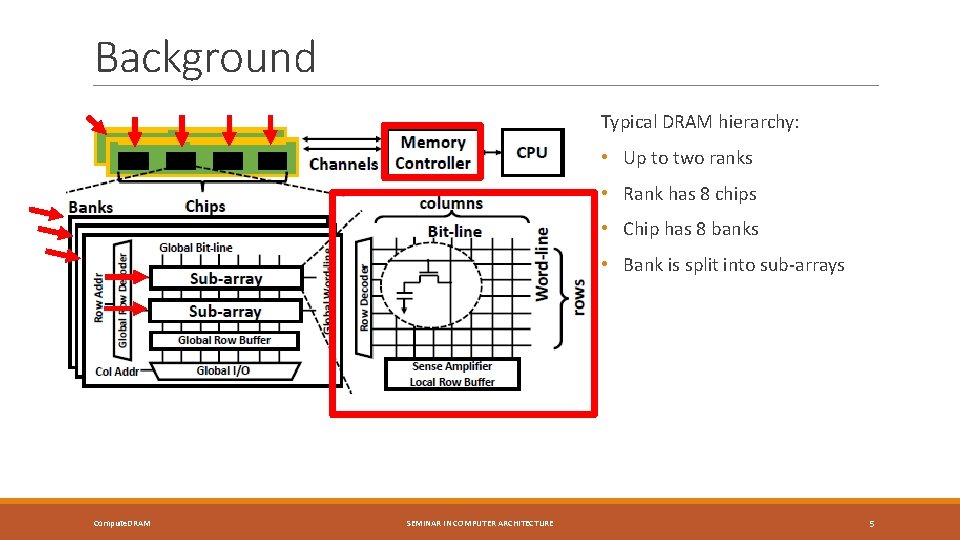
Background Typical DRAM hierarchy: • Up to two ranks • Rank has 8 chips • Chip has 8 banks • Bank is split into sub-arrays Compute. DRAM SEMINAR IN COMPUTER ARCHITECTURE 5

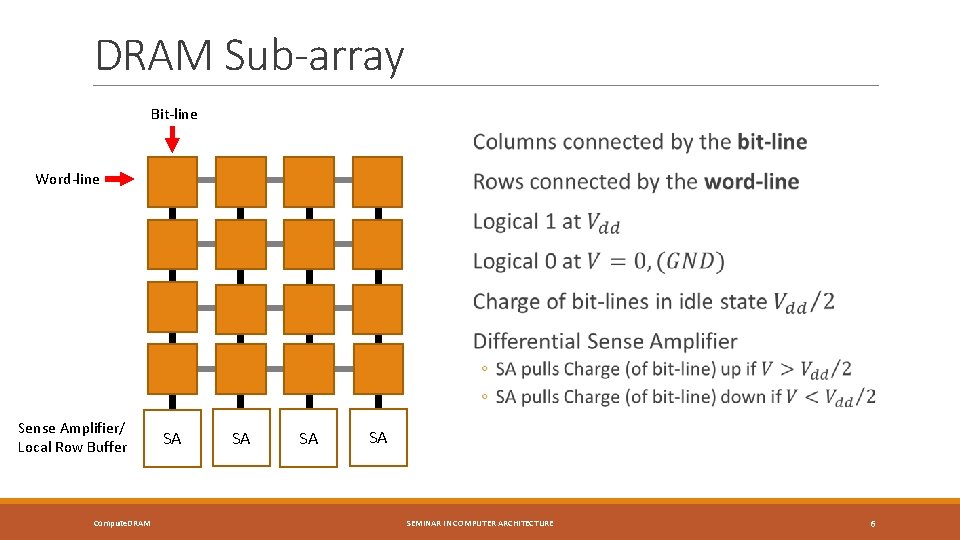
DRAM Sub-array Bit-line Word-line Sense Amplifier/ Local Row Buffer Compute. DRAM SA SA SEMINAR IN COMPUTER ARCHITECTURE 6

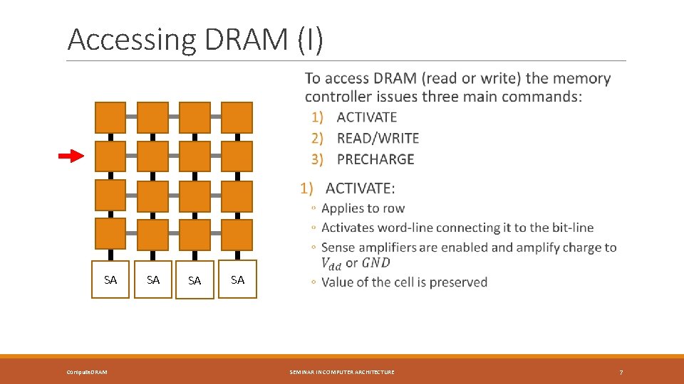
Accessing DRAM (I) SA Compute. DRAM SA SA SA SEMINAR IN COMPUTER ARCHITECTURE 7

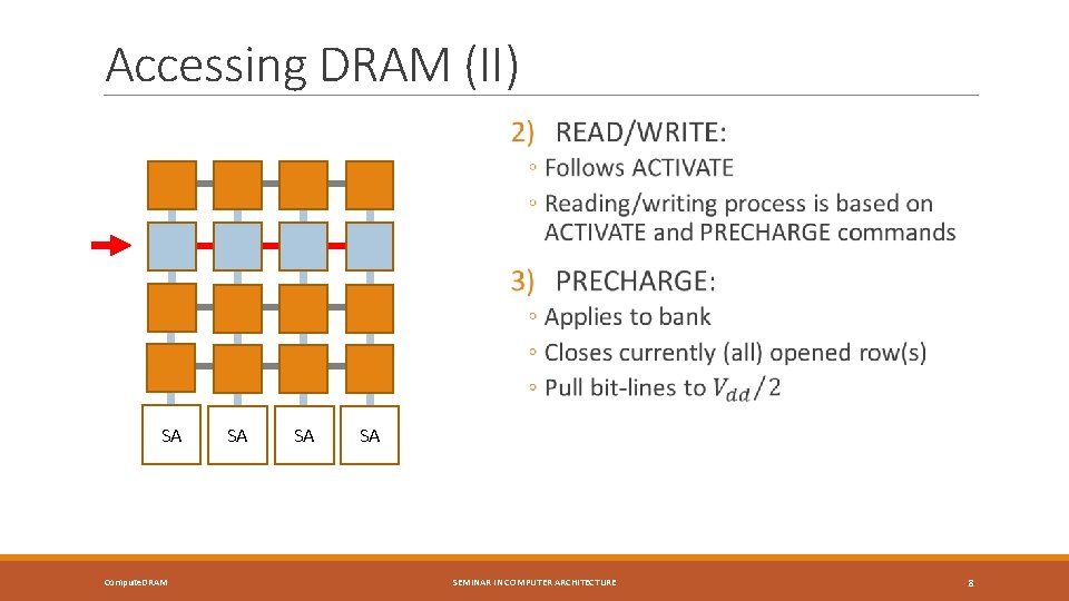
Accessing DRAM (II) SA Compute. DRAM SA SA SA SEMINAR IN COMPUTER ARCHITECTURE 8

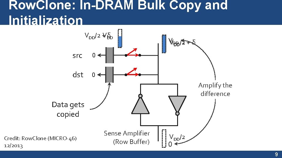
Row. Clone: In-DRAM Bulk Copy and Initialization VDD/2 +VDD δ src 0 dst 0 VVDD DD/2 + δ Amplify the difference Data gets copied Credit: Row. Clone (MICRO-46) 12/2013 Sense Amplifier (Row Buffer) VDD/2 0 9

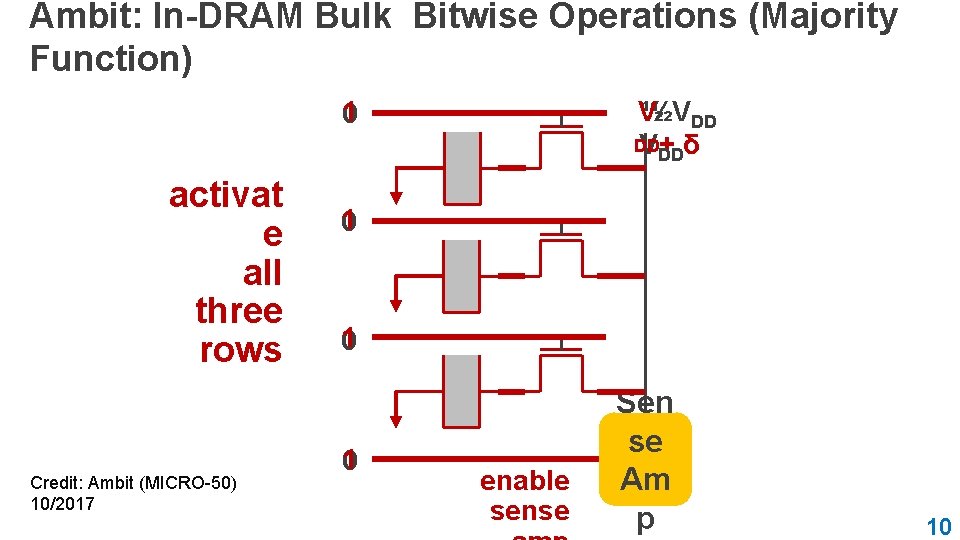
Ambit: In-DRAM Bulk Bitwise Operations (Majority Function) 1 0 activat e all three rows Credit: Ambit (MICRO-50) 10/2017 V ½ ½VDD DD VDD +δ 1 0 1 0 enable sense Sen se Am p 10

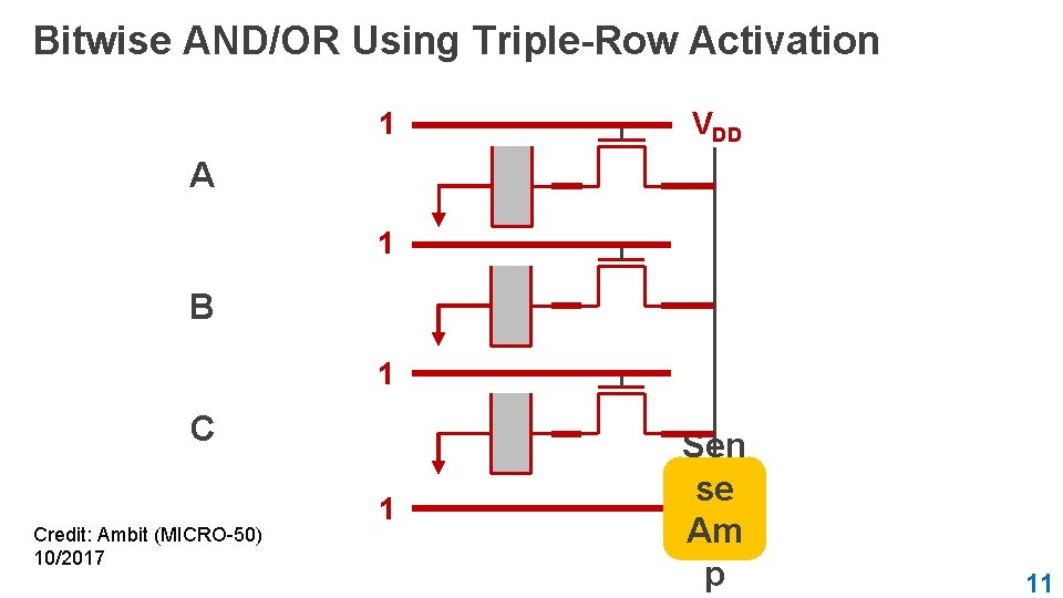
Bitwise AND/OR Using Triple-Row Activation 1 VDD A 1 B 1 C Credit: Ambit (MICRO-50) 10/2017 1 Sen se Am p 11

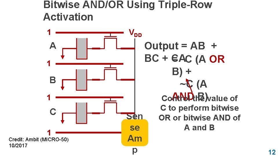
Bitwise AND/OR Using Triple-Row Activation 1 VDD Output = AB + BC + CA = C (A OR B) + ~C (A ANDthe B)value of Control A 1 B 1 Credit: Ambit (MICRO-50) 10/2017 Sen se Am p C to perform bitwise OR or bitwise AND of A and B 12

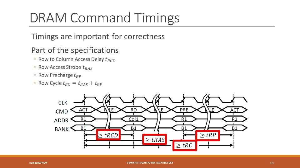
DRAM Command Timings Compute. DRAM SEMINAR IN COMPUTER ARCHITECTURE 13

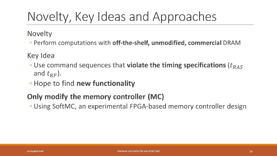
Novelty, Key Ideas and Approaches Compute. DRAM SEMINAR IN COMPUTER ARCHITECTURE 14

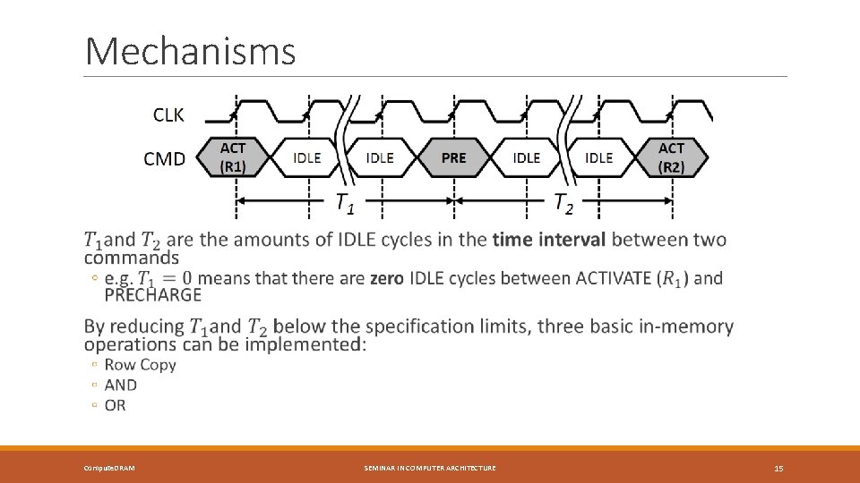
Mechanisms Compute. DRAM SEMINAR IN COMPUTER ARCHITECTURE 15

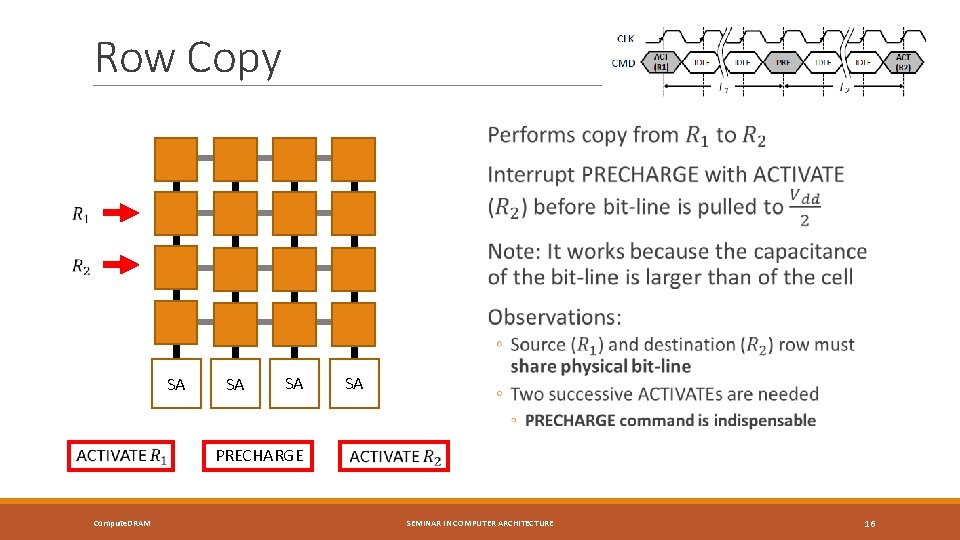
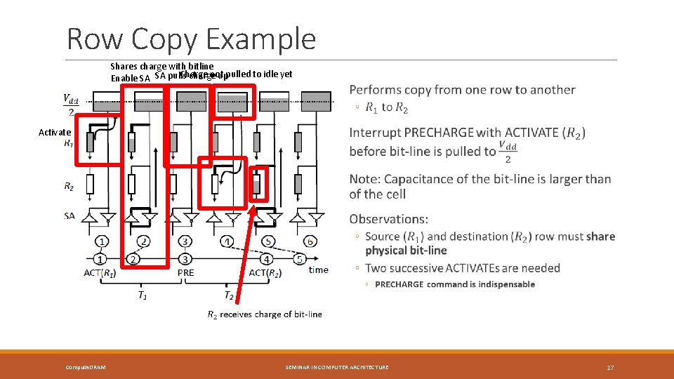
Row Copy SA SA SA PRECHARGE Compute. DRAM SA SEMINAR IN COMPUTER ARCHITECTURE 16

Row Copy Example Shares charge with bitline Charge not pulled to idle yet Enable SA SA pulls charge up Activate Compute. DRAM SEMINAR IN COMPUTER ARCHITECTURE 17

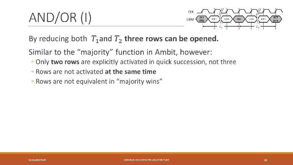
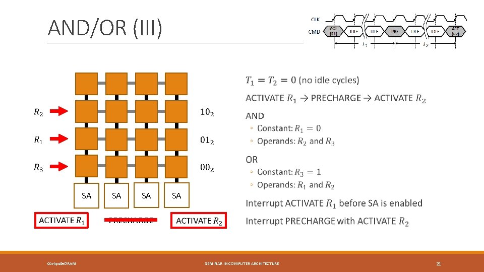
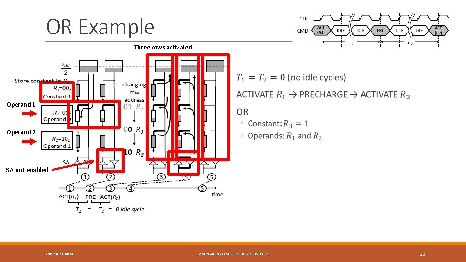
AND/OR (I) Compute. DRAM SEMINAR IN COMPUTER ARCHITECTURE 18

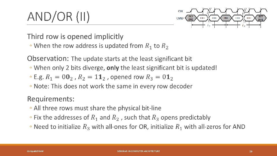
AND/OR (II) Compute. DRAM SEMINAR IN COMPUTER ARCHITECTURE 19

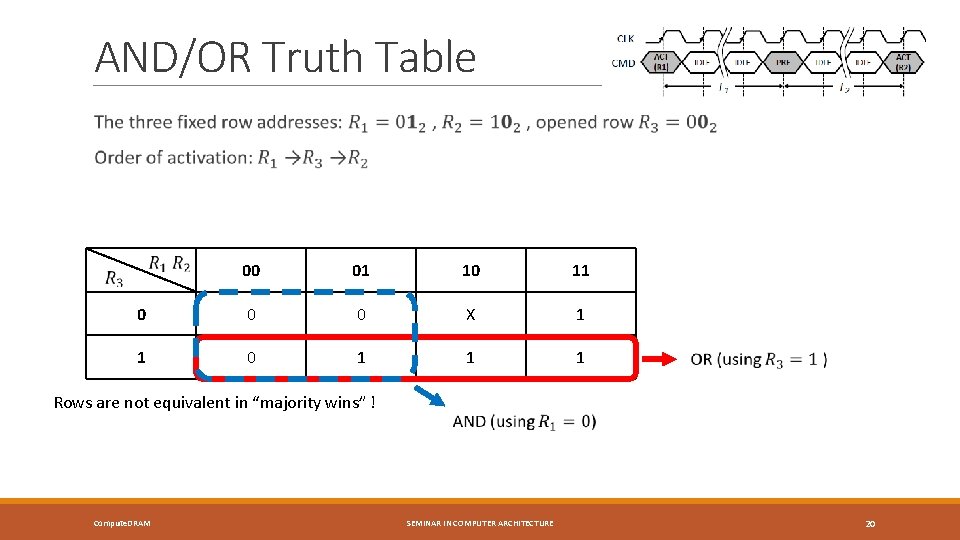
AND/OR Truth Table 00 01 10 11 0 0 0 X 1 1 0 1 1 1 Rows are not equivalent in “majority wins” ! Compute. DRAM SEMINAR IN COMPUTER ARCHITECTURE 20

AND/OR (III) SA SA PRECHARGE Compute. DRAM SA SEMINAR IN COMPUTER ARCHITECTURE 21

OR Example Three rows activated! Operand 1 Operand 2 SA not enabled Compute. DRAM SEMINAR IN COMPUTER ARCHITECTURE 22

Implementations ◦ AND, OR and Row. Copy Arbitrary Computations with Memory ◦ Achieve logical completeness using a pseudo-NOT implementation (always storing the inverse of a value as well) Implementation choices ◦ Computation is performed in first three rows in each sub-array ending with 00, 01, 10. ◦ Operands are saved in rows after the first three and copied using row copy Compute. DRAM SEMINAR IN COMPUTER ARCHITECTURE 23

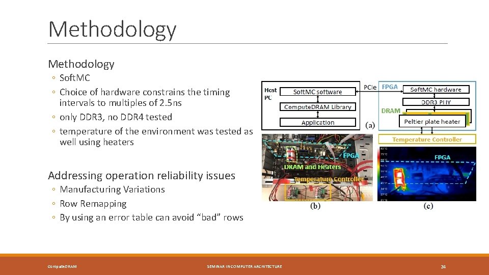
Methodology ◦ Soft. MC ◦ Choice of hardware constrains the timing intervals to multiples of 2. 5 ns ◦ only DDR 3, no DDR 4 tested ◦ temperature of the environment was tested as well using heaters Addressing operation reliability issues ◦ Manufacturing Variations ◦ Row Remapping ◦ By using an error table can avoid “bad” rows Compute. DRAM SEMINAR IN COMPUTER ARCHITECTURE 24

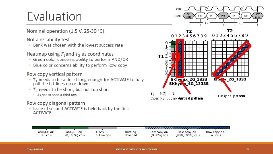
Evaluation Compute. DRAM SEMINAR IN COMPUTER ARCHITECTURE Vertical pattern Diagonal pattern 25

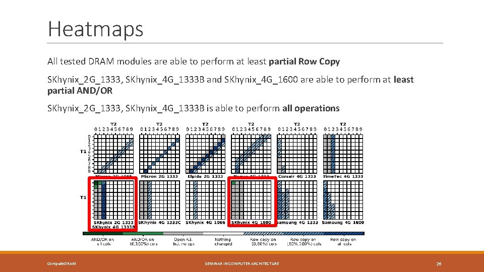
Heatmaps All tested DRAM modules are able to perform at least partial Row Copy SKhynix_2 G_1333, SKhynix_4 G_1333 B and SKhynix_4 G_1600 are able to perform at least partial AND/OR SKhynix_2 G_1333, SKhynix_4 G_1333 B is able to perform all operations Compute. DRAM SEMINAR IN COMPUTER ARCHITECTURE 26

Conclusion Problem: Memory Wall ◦ Moving data from and to memory incurs long access latency ◦ Existing solutions are not feasible (for DRAM manufacturers) Goal: Proof of concept that in-memory computation is possible with unmodified DRAM modules Compute. DRAM ◦ In-memory computation using minimal modifications ◦ Off-the-shelf, unmodified, commercial DRAM ◦ Row Copy, AND and OR: logical completeness by saving inverse values as well ◦ Arbitrary computations made possible using a modified memory controller Results ◦ In-memory computation possible with unmodified DRAM modules ◦ Financially feasible way for DRAM manufacturers to support in-memory compute Compute. DRAM SEMINAR IN COMPUTER ARCHITECTURE 27

Strengths Proof-of-concept works Paper goes even further ◦ Arbitrary computations (implementation is logically complete) ◦ Simple arithmetic example Well written paper Explanations are easy and intuitive to understand Compute. DRAM SEMINAR IN COMPUTER ARCHITECTURE 28

Weaknesses It is not clear what mechanisms follow from observation and what follows from factual knowledge about DRAM ◦ i. e. row address change does not work the same in every row decoder It is not very clear which contribution is made by the paper and which contributions are from Row. Clone/Ambit DRAM is unmodified but a lot of changes are needed in the system Even though it might be clear, performance gains are only mentioned briefly on paper, no charts Compute. DRAM SEMINAR IN COMPUTER ARCHITECTURE 29

Further Readings ØAmbit: In-Memory Accelerator for Bulk Bitwise Operations Using Commodity DRAM Technology Øhttps: //people. inf. ethz. ch/omutlu/pub/ambit-bulk-bitwise-dram_micro 17. pdf ØRow. Clone: Fast and Energy-Efficient In-DRAM Bulk Data Copy and Initialization Øhttps: //users. ece. cmu. edu/~omutlu/pub/rowclone_micro 13. pdf ØDRISA: A DRAM-based Reconfigurable In-Situ Accelerator Øhttps: //www. ece. ucsb. edu/Faculty/selected_pubs/xie/2017 -MICRODRISA%20 DRAM%20 Based%20 Reconfigurable%20 In-Situ%20 Accelerator. pdf ØDr. Acc: a DRAM based Accelerator for Accurate CNN Inference Øhttps: //ieeexplore. ieee. org/document/8465866 ØNeural Cache: Bit-Serial In-Cache Acceleration of Deep Neural Networks Øhttp: //blaauw. engin. umich. edu/wp-content/uploads/sites/342/2019/10/Neural-Cache_-Bit-Serial-In. Cache-Acceleration-of-Deep-Neural-Networks. pdf Compute. DRAM SEMINAR IN COMPUTER ARCHITECTURE 30

Discussion What makes this work (un)practical for actual use? ◦ What further modifications in the system are needed? ◦ What is the main overhead introduced in the implementation? What effect does it have on DRAM manufacturers to support inmemory computation? What type of workloads can benefit from this technology? How can more complex computations be implemented? Compute. DRAM SEMINAR IN COMPUTER ARCHITECTURE 31

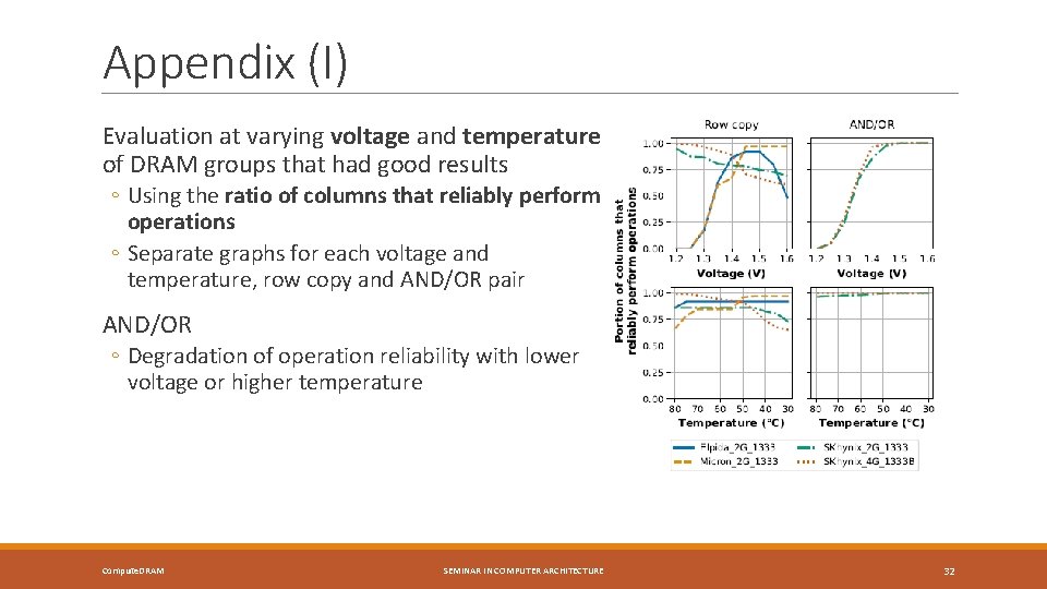
Appendix (I) Evaluation at varying voltage and temperature of DRAM groups that had good results ◦ Using the ratio of columns that reliably perform operations ◦ Separate graphs for each voltage and temperature, row copy and AND/OR pair AND/OR ◦ Degradation of operation reliability with lower voltage or higher temperature Compute. DRAM SEMINAR IN COMPUTER ARCHITECTURE 32

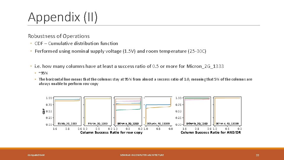
Appendix (II) Robustness of Operations ◦ CDF – Cumulative distribution function ◦ Performed using nominal supply voltage (1. 5 V) and room temperature (25 -30 C) ◦ i. e. how many columns have at least a success ratio of 0. 5 or more for Micron_2 G_1333 ◦ ~95% ◦ The horizontal line means that the columns stay at 95% from almost a success ratio of 1. 0, meaning that 5% of the columns are always unable to perform row copy Compute. DRAM SEMINAR IN COMPUTER ARCHITECTURE 33